 66
66
AMD Ryzen 5 9600X Review - The Best Sub-$300 Gaming CPU
(66 Comments) »Introduction
AMD Ryzen 5 9600X is the latest kid on the block, and the most affordable ticket to the Ryzen 9000 series Granite Ridge desktop processor family powered by the new Zen 5 architecture. The processor is targeted at the upper mid-range, with enough processing muscle on offer for a feature-packed gaming PC build. This processor can be paired with even a high-end graphics card, and play at the highest resolutions, with no noticeable performance drops compared to processors from a higher segment. It's only when you combine gaming with streaming, video effects and overlays on the side like popular creators do, that you might miss having more cores. AMD is positioning the Ryzen 5 9600X against its main rival from the Intel camp, the Core i5-14600K.

The AMD Ryzen 5 9600X is a classic multicore processor with a 6-core/12-thread configuration. The company continues to stick to CPU core counts from its past three generations, as each new generation of Zen delivered on IPC gains, energy efficiency, and competitiveness with Intel in key client desktop applications such as AAA games, and popular creativity suites. AMD held a technological edge over Intel in foundry process each generation thanks to its partnership with TSMC, so the company never really needed efficiency cores (E-cores), either to shore up core counts, or reduce power-draw in light workloads.
The new Zen 5 microarchitecture is claimed by AMD to offer a roughly 16% increase in IPC over Zen 4, which when paired with the nominal increases in clock speeds, should account for increased gaming performance over the previous generation, at comparable power. Besides the new architecture, AMD is also building its CPU core complex dies (CCDs) on the more refined 4 nm TSMC N4P foundry node, which is claimed to offer 22% improved power characteristics over the 5 nm TSMC N5 node that AMD built its Zen 4 CCDs on. Both the Ryzen 5 9600X, and the 8-core Ryzen 7 9700X that are launching today come with a 65 W TDP, compared to the 105 W that the 7600X and 7700X launched with.
The new Zen 5 microarchitecture introduces several design updates across the length and breadth of the core, as you'll learn on the next page. There is a larger share of engineering focus on the core's execution engine, which includes the integer and floating point units. The FPU is now bolstered with a real 512-bit data-path, compared to the dual-pumped 256-bit data-path on Zen 4, which AMD claims increases performance of 512-bit SIMD workloads by 20-35%, when using instruction-sets such as AVX-512, VNNI, etc., AMD also worked to increase the intra-core bandwidth, and made all on-die caches faster.
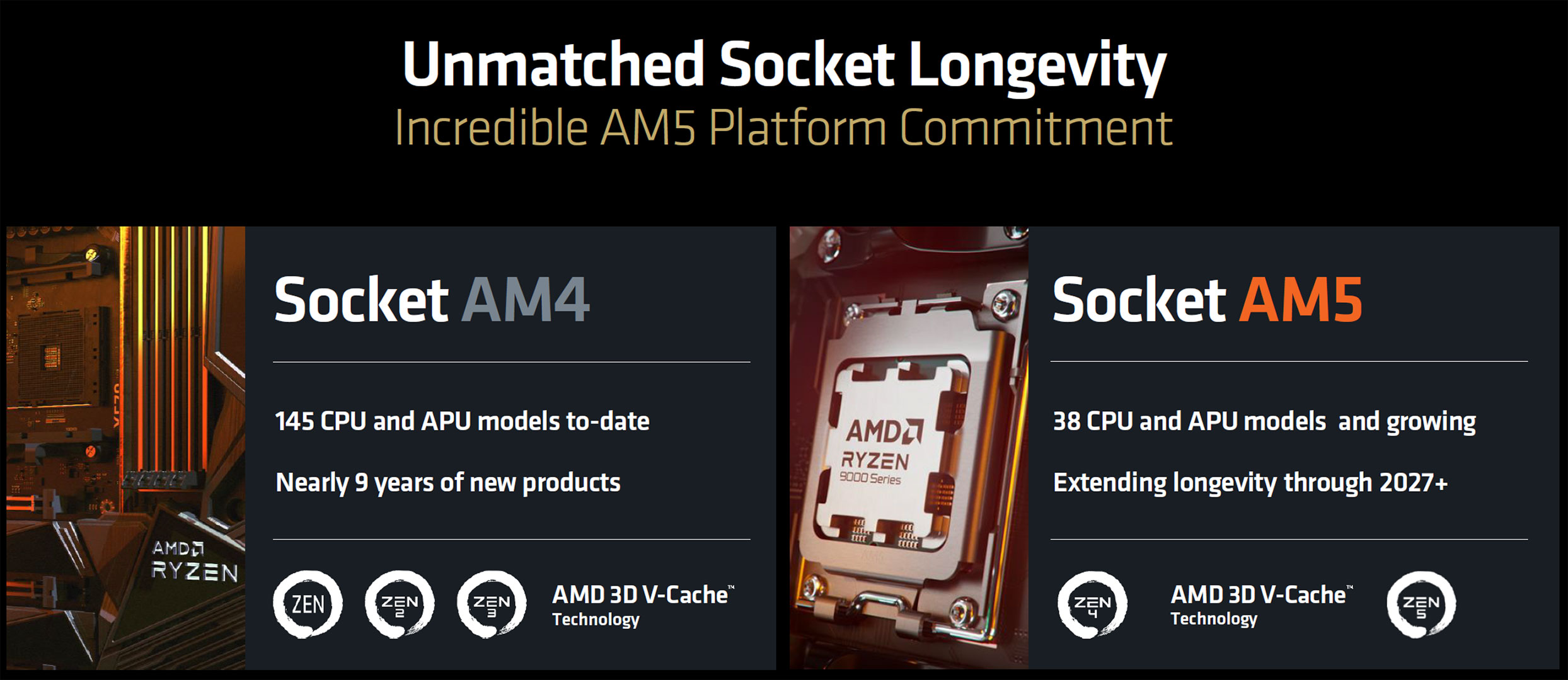
The Ryzen 5 9600X ticks at a base frequency of 3.90 GHz, with a maximum boost frequency of 5.40 GHz. Each of its six Zen 5 cores comes with 1 MB of dedicated L2 cache, and the six cores share 32 MB of L3 cache. AMD has given this chip a TDP of 65 W. Since it's built for the existing Socket AM5, the 9600X is compatible with all AMD 600-series chipset motherboards with a BIOS update, as well as being drop-in compatible with motherboards based on the upcoming 800-series chipset. AMD is pricing the Ryzen 5 9600X at $280. This is $20 less than what the 7600X launched at.
Short 9-Minute Summary of this Review
Our goal with the videos is to create short summaries, not go into all the details and test results, which can be found on the following pages of this review.
| Price | Cores / Threads | Base Clock | Max. Boost | L3 Cache | TDP | Architecture | Process | Socket | |
|---|---|---|---|---|---|---|---|---|---|
| Intel Core i5 | |||||||||
| Core i5-12400F | $150 | 6 / 12 | 2.5 GHz | 4.4 GHz | 18 MB | 65 W | Alder Lake | 10 nm | LGA 1700 |
| Core i5-13400F | $170 | 6+4 / 16 | 2.5 / 1.8 GHz | 4.6 / 3.3 GHz | 20 MB | 65 W | Raptor Lake | 10 nm | LGA 1700 |
| Core i5-12600K | $245 | 6+4 / 16 | 3.7 / 2.8 GHz | 4.9 / 3.6 GHz | 20 MB | 125 W | Alder Lake | 10 nm | LGA 1700 |
| Core i5-13600K | $240 | 6+8 / 20 | 3.5 / 2.6 GHz | 5.1 / 3.9 GHz | 24 MB | 125 W | Raptor Lake | 10 nm | LGA 1700 |
| Core i5-14600K | $300 | 6+8 / 20 | 3.5 / 2.6 GHz | 5.3 / 4.0 GHz | 24 MB | 125 W | Raptor Lake | 10 nm | LGA 1700 |
| AMD Ryzen 5 | |||||||||
| Ryzen 5 8500G | $160 | 6 / 12 | 3.5 GHz | 5.0 GHz | 16 MB | 65 W | Phoenix 2 | 4 nm | AM5 |
| Ryzen 5 5600X | $135 | 6 / 12 | 3.7 GHz | 4.6 GHz | 32 MB | 65 W | Zen 3 | 7 nm | AM4 |
| Ryzen 5 7600 | $185 | 6 / 12 | 3.8 GHz | 5.1 GHz | 32 MB | 65 W | Zen 4 | 5 nm | AM5 |
| Ryzen 5 7600X | $195 | 6 / 12 | 4.7 GHz | 5.3 GHz | 32 MB | 105 W | Zen 4 | 5 nm | AM5 |
| Ryzen 5 9600X | $280 | 6 / 12 | 3.9 GHz | 5.4 GHz | 32 MB | 65 W | Zen 5 | 4 nm | AM5 |
| Intel Core i7 | |||||||||
| Core i7-12700K | $315 | 8+4 / 20 | 3.6 / 2.7 GHz | 5.0 / 3.8 GHz | 25 MB | 125 W | Alder Lake | 10 nm | LGA 1700 |
| Core i7-13700K | $320 | 8+8 / 24 | 3.4 / 2.5 GHz | 5.4 / 4.2 GHz | 30 MB | 125 W | Raptor Lake | 10 nm | LGA 1700 |
| Core i7-14700K | $380 | 8+12 / 28 | 3.4 / 2.5 GHz | 5.6 / 4.3 GHz | 33 MB | 125 W | Raptor Lake | 10 nm | LGA 1700 |
| AMD Ryzen 7 | |||||||||
| Ryzen 7 5700G | $160 | 8 / 16 | 3.8 GHz | 4.6 GHz | 16 MB | 65 W | Zen 3 + Vega | 7 nm | AM4 |
| Ryzen 7 5700X | $160 | 8 / 16 | 3.4 GHz | 4.6 GHz | 32 MB | 65 W | Zen 3 | 7 nm | AM4 |
| Ryzen 7 7700 | $280 | 8 / 16 | 3.8 GHz | 5.3 GHz | 32 MB | 65 W | Zen 4 | 5 nm | AM5 |
| Ryzen 7 7700X | $290 | 8 / 16 | 4.5 GHz | 5.4 GHz | 32 MB | 105 W | Zen 4 | 5 nm | AM5 |
| Ryzen 7 9700X | $360 | 8 / 16 | 3.8 GHz | 5.5 GHz | 32 MB | 65 W | Zen 5 | 4 nm | AM5 |
| Ryzen 7 5800X | $175 | 8 / 16 | 3.8 GHz | 4.7 GHz | 32 MB | 105 W | Zen 3 | 7 nm | AM4 |
| Ryzen 7 5800X3D | $340 | 8 / 16 | 3.4 GHz | 4.5 GHz | 96 MB | 105 W | Zen 3 | 7 nm | AM4 |
| Ryzen 7 7800X3D | $370 | 8 / 16 | 4.2 GHz | 5.0 GHz | 96 MB | 120 W | Zen 4 | 5 nm | AM5 |
| Intel Core i9 | |||||||||
| Core i9-12900K | $425 | 8+8 / 24 | 3.2 / 2.4 GHz | 5.2 / 3.9 GHz | 30 MB | 125 W | Alder Lake | 10 nm | LGA 1700 |
| Core i9-13900K | $445 | 8+16 / 32 | 3.0 / 2.2 GHz | 5.8 / 4.3 GHz | 36 MB | 125 W | Raptor Lake | 10 nm | LGA 1700 |
| Core i9-14900K | $555 | 8+16 / 32 | 3.2 / 2.4 GHz | 6.0 / 4.4 GHz | 36 MB | 125 W | Raptor Lake | 10 nm | LGA 1700 |
| AMD Ryzen 9 | |||||||||
| Ryzen 9 5900X | $265 | 12 / 24 | 3.7 GHz | 4.8 GHz | 64 MB | 105 W | Zen 3 | 7 nm | AM4 |
| Ryzen 9 7900 | $370 | 12 / 24 | 3.7 GHz | 5.4 GHz | 64 MB | 65 W | Zen 4 | 5 nm | AM5 |
| Ryzen 9 7900X | $360 | 12 / 24 | 4.7 GHz | 5.6 GHz | 64 MB | 170 W | Zen 4 | 5 nm | AM5 |
| Ryzen 9 7900X3D | $395 | 12 / 24 | 4.4 GHz | 5.6 GHz | 128 MB | 120 W | Zen 4 | 5 nm | AM5 |
| Ryzen 9 9900X | $500 | 12 / 24 | 4.4 GHz | 5.6 GHz | 64 MB | 120 W | Zen 5 | 4 nm | AM5 |
| Ryzen 9 5950X | $355 | 16 / 32 | 3.4 GHz | 4.9 GHz | 64 MB | 105 W | Zen 3 | 7 nm | AM4 |
| Ryzen 9 7950X | $525 | 16 / 32 | 4.5 GHz | 5.7 GHz | 64 MB | 170 W | Zen 4 | 5 nm | AM5 |
| Ryzen 9 7950X3D | $530 | 16 / 32 | 4.2 GHz | 5.7 GHz | 128 MB | 120 W | Zen 4 | 5 nm | AM5 |
| Ryzen 9 9950X | $650 | 16 / 32 | 4.3 GHz | 5.7 GHz | 64 MB | 170 W | Zen 5 | 4 nm | AM5 |
Architecture
The AMD Ryzen 9000 series desktop processors, including the 9700X, 9600X, and the upcoming 9950X and 9900X, are based on the new Granite Ridge chiplet-based solution. The CPU complex dies (CCDs) are where all the innovation is focussed, as this is where the Zen 5 CPU cores are located. The rest of the processor is made up of the client I/O die (cIOD), which is carried over from the previous generation so that AMD could save on development costs. AMD built the new-generation CCD on the 4 nm TSMC N4P foundry node, an upgrade from the 5 nm TSMC N5 node, with over 22% power improvement, and 6% transistor density improvements. The CCDs are roughly the same size as the Zen 4 CCDs, and fit in nicely with the substrate floor-plan of the Granite Ridge package.
AMD has retained the CPU core counts of its previous generation, the company continues to not be baited into a core-count war with Intel, triggered by its pivot to heterogeneous multicore and tiny E-cores that it can cram many of into its client processors. The Ryzen 9 9950X is the company's flagship part for this generation, and is a 16-core/32-thread chip, with two CCDs. The 9900X is 12-core/24-thread, with two CCDs, and two cores disabled per CCD. The Ryzen 7 9700X is a single CCD part, as is the Ryzen 5 9600X, which comes with two cores disabled, while retaining the full 32 MB L3 cache on the CCD.
The Zen 5 Core
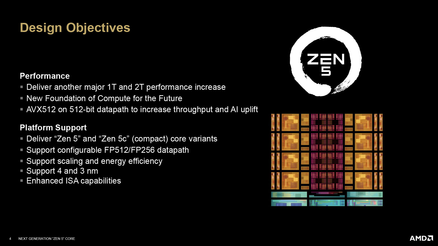
With the I/O and packaging aspects of Granite Ridge covered by carrying over the cIOD and existing Socket AM5 infrastructure, all of AMD's engineering attention is on the 4 nm CCD, and specifically, the Zen 5 CPU cores, since there's not much else on the CCD besides them. It's been AMD's endeavor to give consumers a single-thread performance uplift in the form of an IPC uplift, with each new generation of Zen. These generational IPC uplifts range between 10-19%, and with Zen 5, the company wants you to expect a roughly 16% IPC uplift over Zen 4. AMD designed the Zen 5 core to be "forward-facing" with support for instruction sets that will become more relevant with the advent of AI acceleration into the client space. While the Granite Ridge processor itself lacks an NPU and won't accelerate Copilot+, the Zen 5 cores are designed to boost the workflow of AI software developers and researchers, besides machines that use discrete accelerators, since the CPU-end (software end) of the AI stack can benefit from new capabilities on the cores.
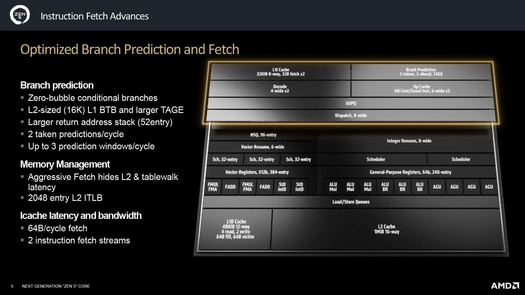
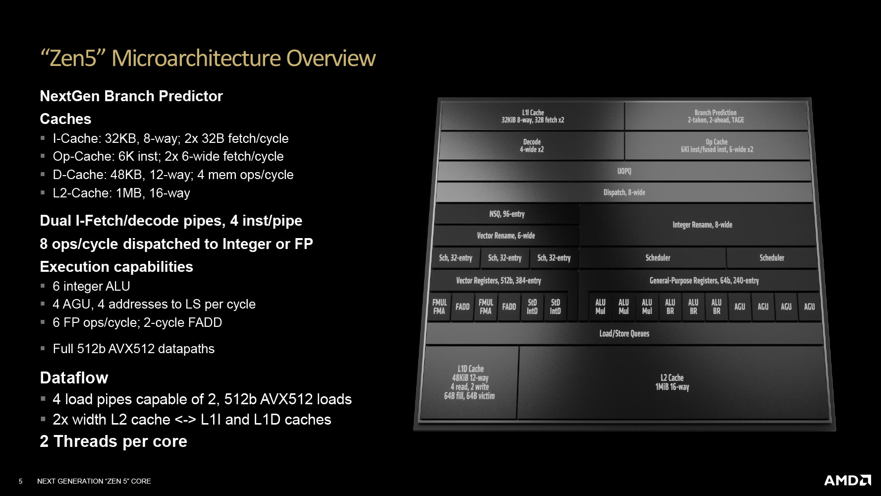
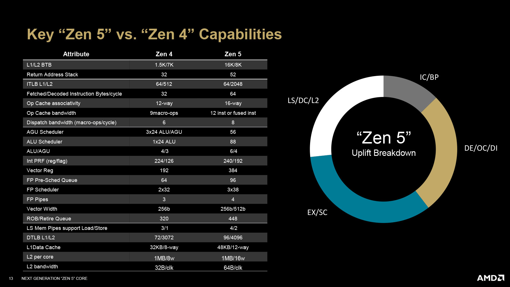
Zen 5 sees AMD update practically all key areas of the CPU core, including the front-end with its branch prediction unit, the various caches within the core, the fetch/decode pipelines, the execution engine, and the load/store. The front-end sees an updated branch prediction unit. This new BP ensures zero-bubble conditional branches to save clock cycles from mispredictions; a large 16 KB L1 BTB, and a larger tagged-geometric length predictor; a larger 52-entry return address stack, compared to 32-entry on Zen 4; a 16-way Op Cache associativity, compared to 12-way on Zen 4, and a 33% increase in Op Cache and dispatch bandwidth. The BP supports up to 3 prediction windows per cycle, compared to 2 on Zen 4. The L2 and tablewalker latency is obscured with the new aggressive fetch unit. The L2 ITLB supports 2,048 entries, compared to just 512 on the Zen 4 core. The L1 instruction cache sees bandwidth and latency improvements, along with two independent instruction fetch streams.
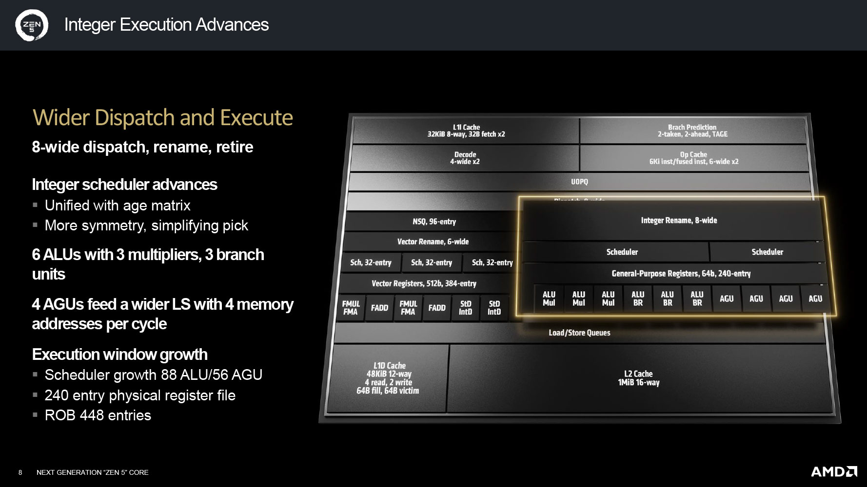
As with every traditional x86 CPU core, the execution unit is segregated into Integer and Floating Point units. The Integer engine features an 8-wide dispatch/retire/rename queue depth. The integer scheduler has more "symmetry" to simplify pick operations. It features 6 ALUs with 3 multipliers, and 3 branch units; besides 4 AGUs. The AGU scheduler supports 56 entries, and the ALU scheduler 88, compared to 3x 24-entry ALU+AGU combined scheduling, with a 24-entry dedicated ALU scheduler. The physical register file is up to 240/192 entries from 224/126 on Zen 4. The ROB retire queue buffer holds 448 entries, compared to 320 on Zen 4.
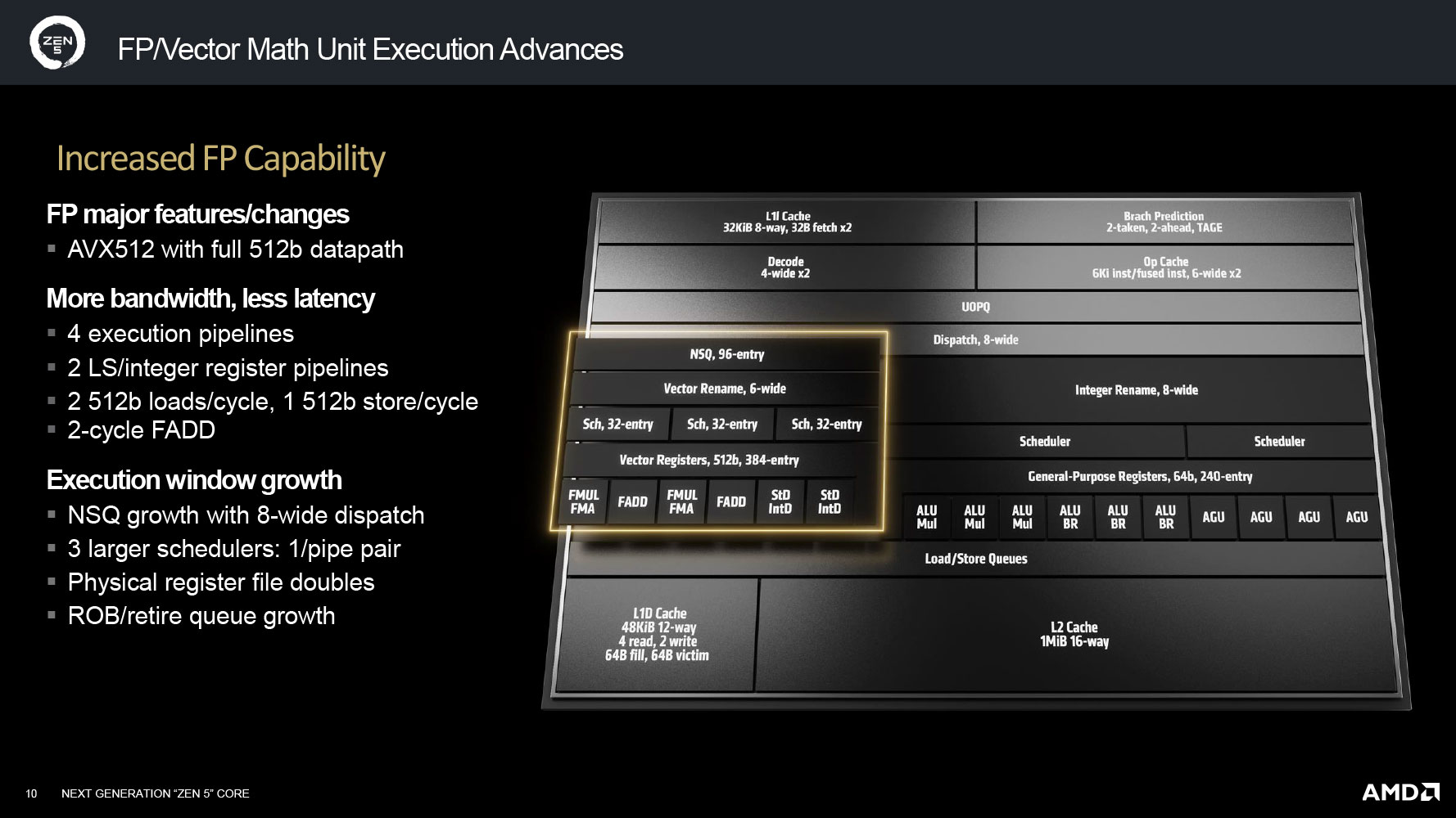
The floating point unit is where Zen 5 seems to have a major design focus. Zen 5 is designed to execute AVX-512 instructions over a full 512-bit data-path, compared to Zen 4, which uses a dual-pumped 256-bit data-path. This should significantly speed up AVX-512, VNNI, and other instructions relevant to AI acceleration on the CPU core. The FPU has four execution pipelines with two LS/integer register pipes. It supports two 512-bit loads, and one 512-bit store per cycle, and a 2-cycle FADD. There are updates to the FPU's execution window.
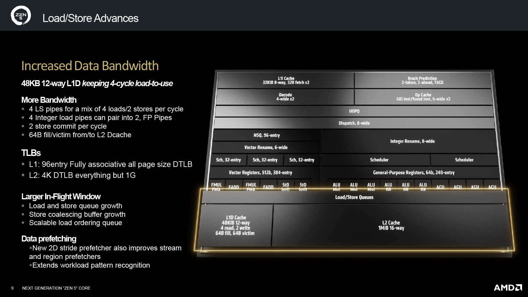
The load/store unit sees several improvements to meet the growth in bandwidth requirements of the execution engine. To begin with, the L1 data cache has been enlarged to 48 KB 12-way, up from 32 KB 8-way on Zen 4. Besides this enlargement, there are improvements to the load/store pipes, with a mix of 4 loads and 2 stores per cycle. Its four integer load pipes can pair into FP pipe. The bandwidth to the L2 cache has been improved.
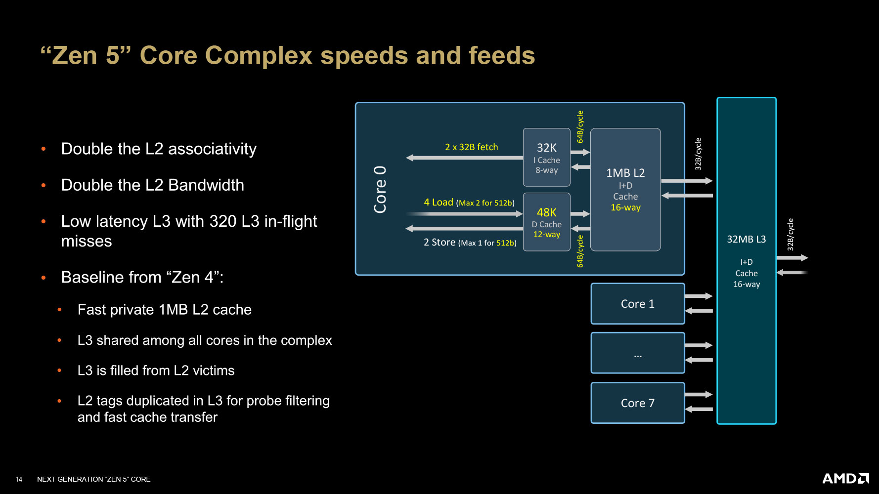
The core's dedicated L2 cache remains 1 MB in size from the previous generation, but AMD says that it has doubled the associativity and bandwidth of this cache over the one Zen 4 comes with. While AMD has retained 32 MB as the standard on-die L3 cache size, which it shares among the 8 cores on the CCD, it has worked to reduce the cache's latency along with tracking up to 320 L3 in-flight misses.
Granite Ridge SoC Features
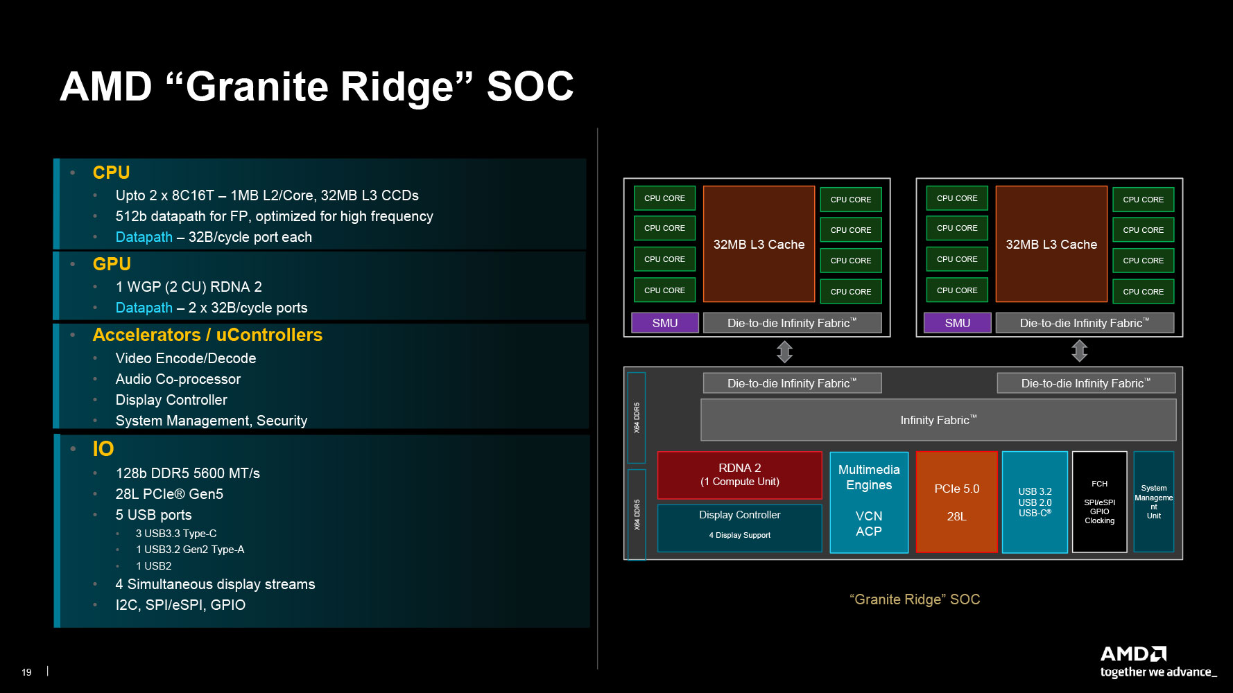
Depending on the processor model, the chip features one or two CCDs, each with 8 Zen 5 cores, 32 MB of L3 cache, an SMU, and an Infinity Fabric interface, with 32 B/cycle read and 16 B/cycle write bandwidth, to the client I/O die (cIOD). The cIOD uses Infinity Fabric as an ether to connect all the various SoC components of the processor, the two most important of which are the dual-channel DDR5 memory controllers (160-bit including ECC), and the 28-lane PCI-Express 5.0 root complex.
AMD provides a basic iGPU with Granite Ridge, just like it did with Raphael. This is based on the older RDNA 2 graphics architecture, and consists of just one workgroup processor (WGP), or just two compute units (CU), worth 128 stream processors. This iGPU talks to a display controller that supports up to four displays; and a multimedia engine that can accelerate decode of H.265 and AV1.
There's also an integrated USB interface, with support for USB 3.2 (up to two 10 Gbps ports), a couple of USB 2.0 ports, and legacy interfaces, including SPI, eSPI, GPIO, I2C, etc. The client I/O die is built on the 6 nm foundry node, as many of these components don't really benefit from the latest 4 nm node. The cIOD of Granite Ridge is carried over from Raphael, with only some microcode updates that give it native support for DDR5-5600 (Ryzen 7000 natively supported DDR5-5200), various overclocking speeds over AMD EXPO, and support for higher DDR5 overclocking memory speeds using a 1:2 divider between the FCLK and MCLK.
AMD X870E, X870, B850, and B840 Chipsets
Along with the Ryzen 9000 Granite Ridge series, AMD is debuting the new AMD 800 series desktop motherboard chipset family. The processors are built in the existing Socket AM5, and as such are compatible with any AMD 600-series chipset motherboard with a BIOS update. Helping things along are the fact that nearly every AM5 motherboard comes with USB BIOS Flashback, which should let you blind-flash your BIOS even if you have an "incompatible" processor.
AMD hasn't changed the I/O of its processors, as we detailed in the previous page, but identified the reasons why some of its 600-series chipset models were vastly outselling the others. Market studies showed that enthusiasts are drawn to the top X670E, and the rest of the crowd to the well-rounded B650, with no takers for the X670 and B650E. AMD set out to correct these by shuffling up the feature-sets among its 800-series chipset models, while also using the occasion to standardize a few I/O features, such as USB4, and encouraging its motherboard partners to provide new connectivity options, such as Wi-Fi 7.
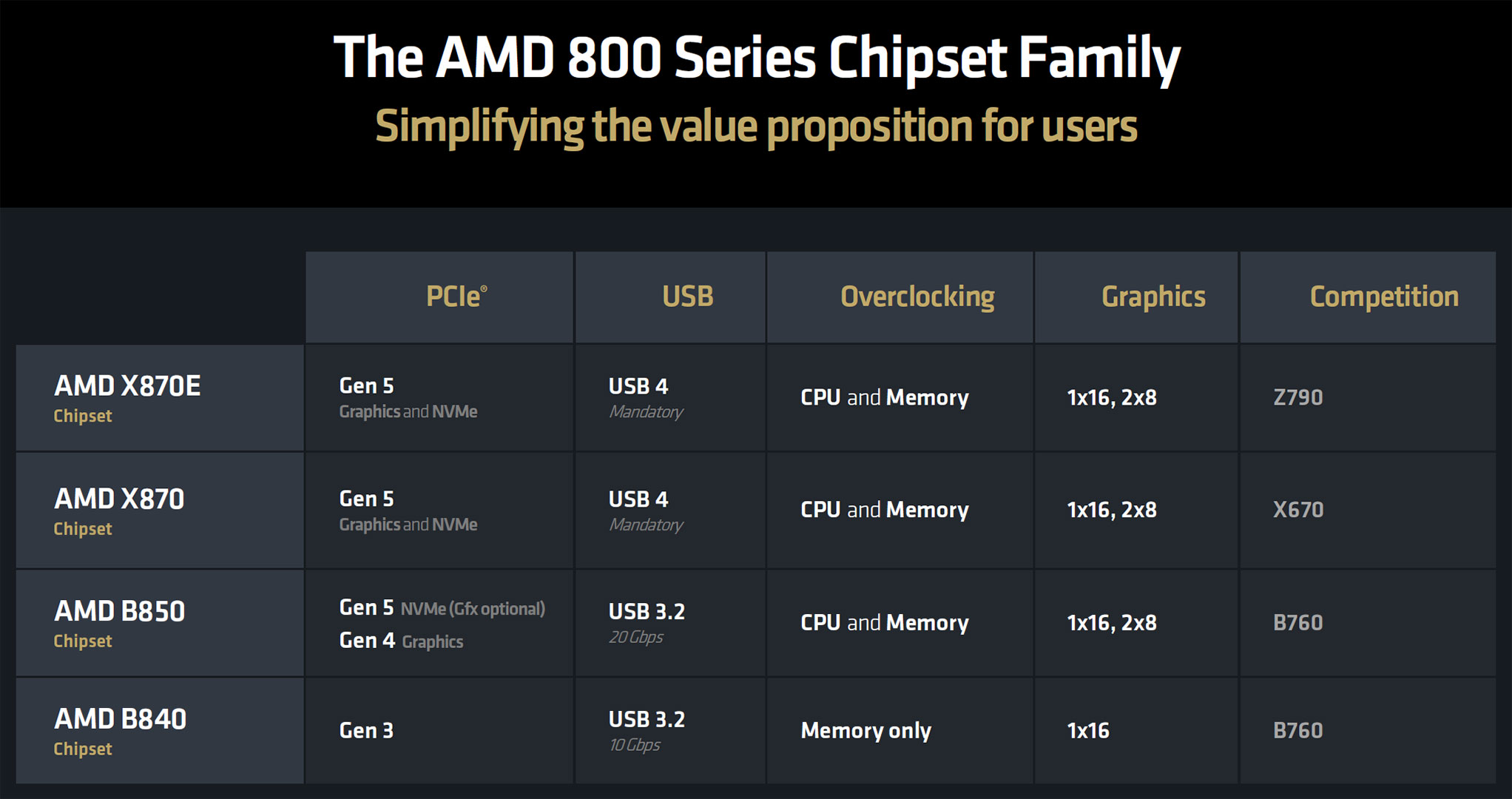
The AMD X870E leads the pack in terms of connectivity. It is a dual-chip solution, much like the X670E and X670. You are assured PCI-Express Gen 5 for the x16 PEG slot, as well as the CPU-attached NVMe slots; while the chipset puts out up to 16 Gen 4 PCIe lanes. Also, motherboard designers are mandated to provide 40 Gbps USB4 connectivity.
The X870 (non-E) is a lite version of this chipset, and is a single-chip solution, much like B650E. You'll still get PCI-Express Gen 5 x16 for the PEG slot, as well as Gen 5 for the CPU-attached NVMe slots, however the chipset only puts out 8 Gen 4 PCIe lanes for general purpose I/O. Much like X870E, with the X870, you are assured of USB4 connectivity.
The B850 is a successor of B650. It is a single-chip solution, just like X870, but here, motherboard vendors are allowed to wire out the PCI-Express x16 PEG slot as Gen 4. The CPU-attached NVMe interfaces, however, should remain Gen 5 capable. Motherboard vendors can provide Gen 5 x16 PEG if they want (it's optional). USB4 isn't mandatory. So a vendor can design an X870 motherboard and simply pull out the USB4 interface to label the board as B850. Much like the X870E and X870, the B850 supports both CPU and memory overclocking.
Lastly, there's B840, an entry-level chipset meant to succeed the A620 and A620A. The PCI-Express x16 PEG runs at primitive Gen 3 mode. The chipset puts out just 8 Gen 3 lanes. There's no CPU overclocking support, only memory. The B840 should hence power the vast majority of entry-level or commercial desktop motherboards.
Overclocking
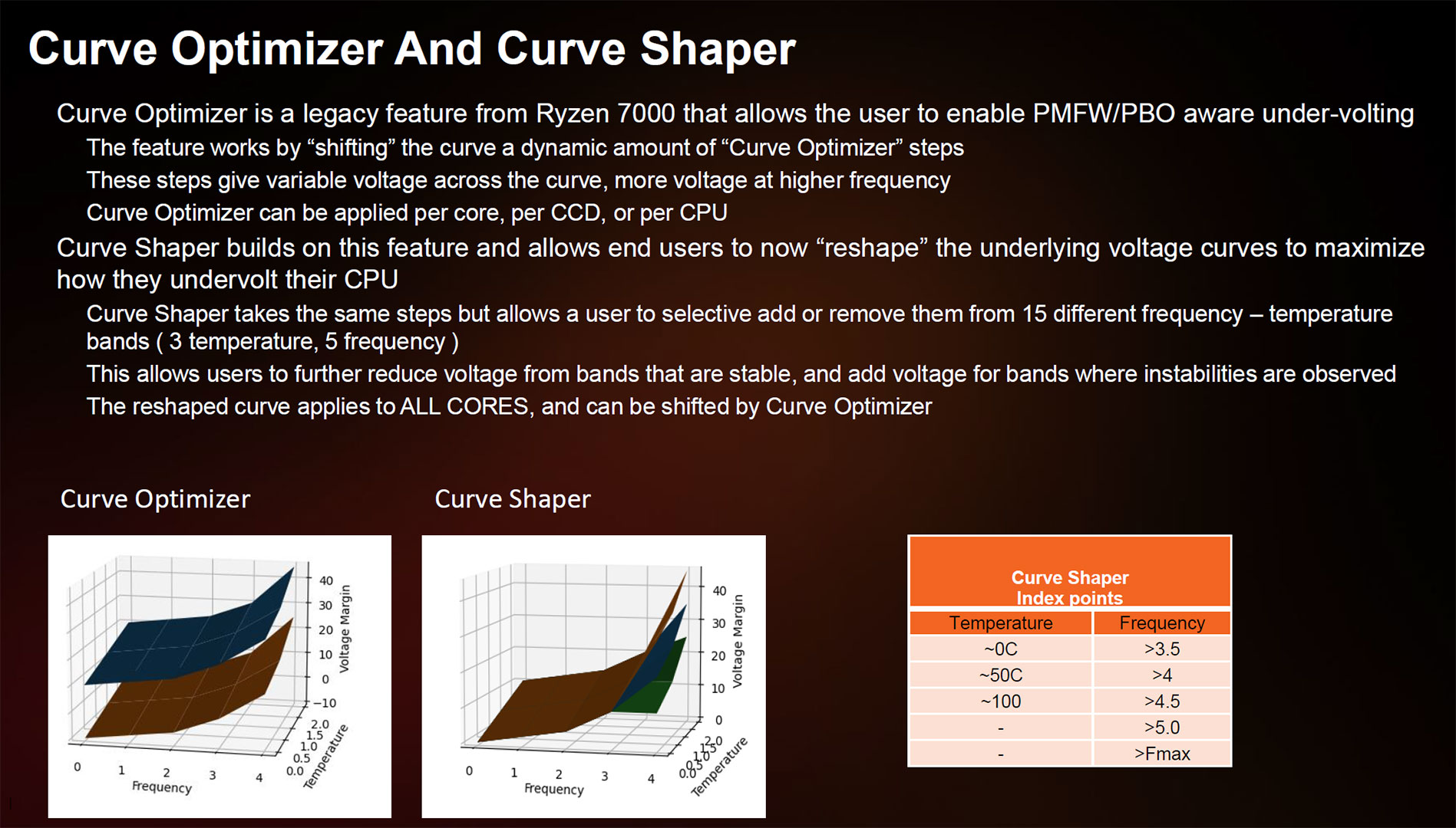
Curve Shaper is a new feature being introduced with Ryzen 9000 series processors. It's part of the AMD CBS, which means it can be configured in the UEFI setup program, should the motherboard vendor choose to have a GUI there, or using Ryzen Master on Windows. Curve Optimizer enabled PBO and PMFW-aware under-volting, while Curve Shaper lets end-users reshape the underlying voltage curves to fine tune voltage control across different workloads and frequencies.
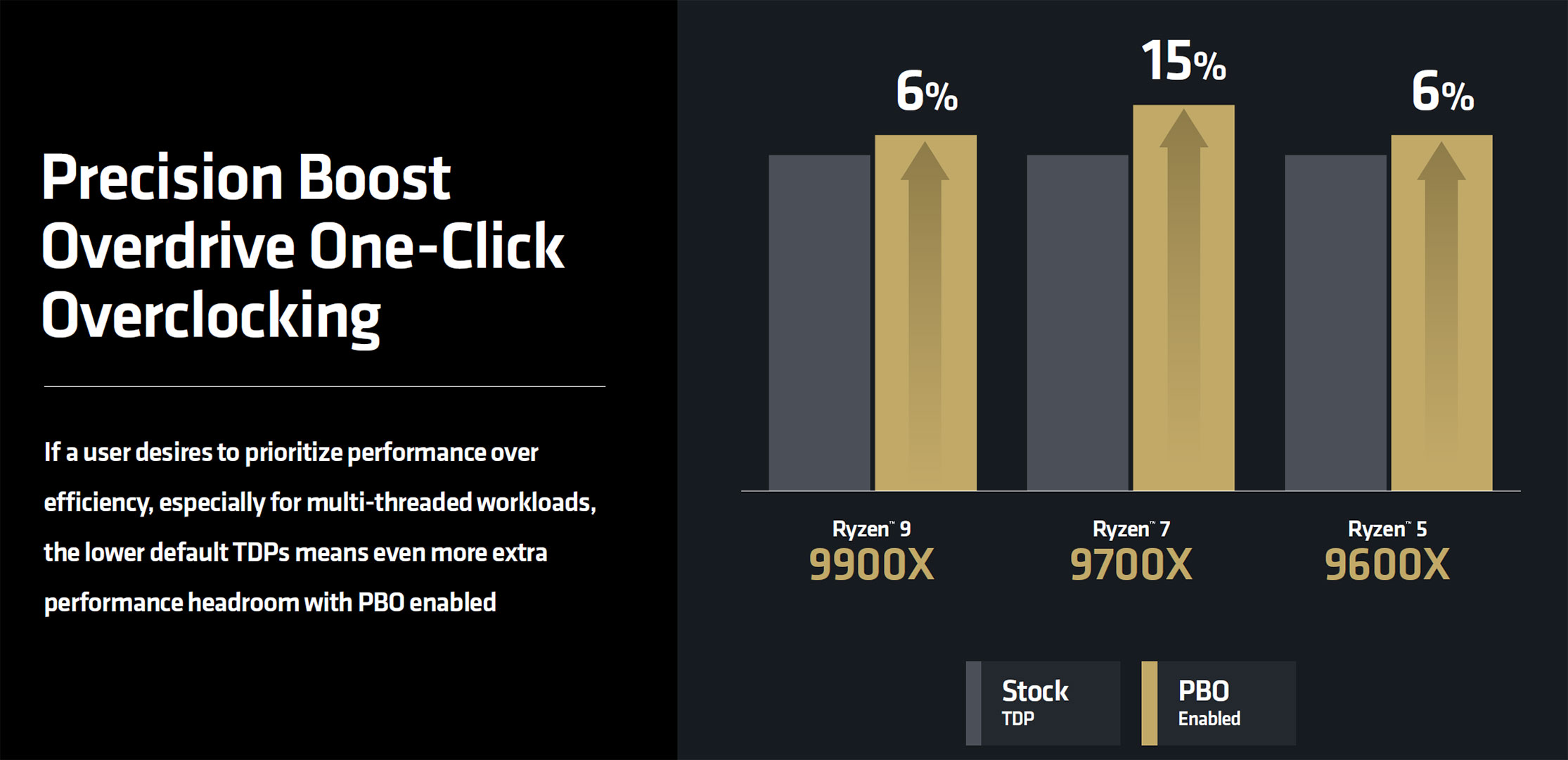
A side effect of giving processor models such as the 9900X (120 W), 9700X (65 W), and 9600X lower TDP than their predecessors, the 7900X (170 W), and 7700X (105 W), is that Precision Boost Overdrive (PBO) now scoops out more performance, as it raises the package power for the processors. AMD claims further performance gains of 6% for the 9900X, and up to 15% for the 9700X (which goes to show that 65 W was too conservative).
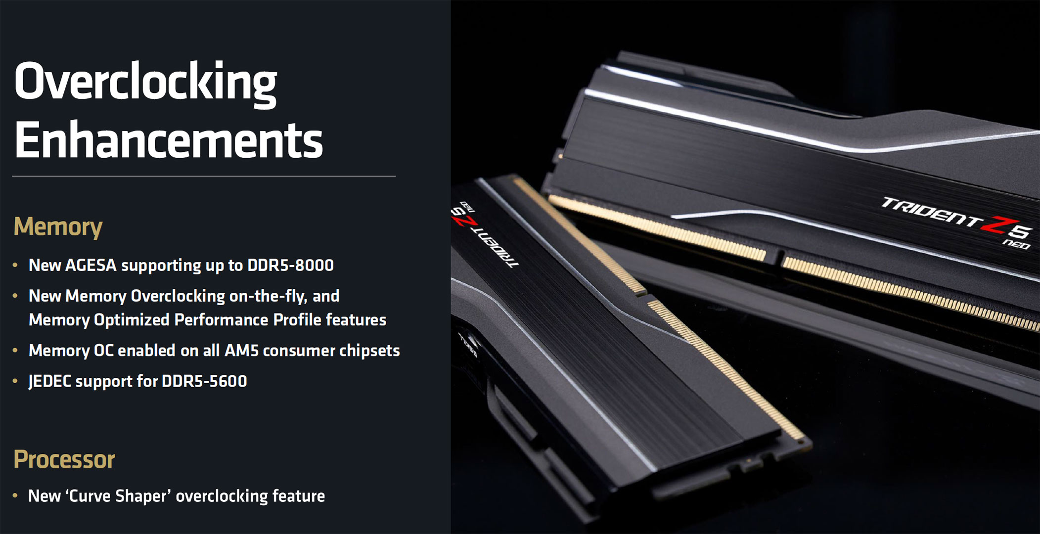
The native DDR5 speed has been increased to DDR5-5600, and support has been added for overclocked memory as fast as DDR5-8000. To achieve this, a 1:2 clock divider is engaged between FCLK and MCLK as soon as memory clock is set higher than DDR5-6000. You may manually force a 1:1 divider "and with some luck" you will be able to run DDR5-6400—essentially the same as with Zen 4. The DDR5-8000 support is being released by AMD as an update to the AGESA microcode, for motherboard vendors to integrate with even their older AMD 600-series chipset products. There should be a new wave of enthusiast PC memory with AMD EXPO profiles for DDR5-8000 and everything under (such as DDR5-7200, DDR5-6800, etc.). In terms of performance it will be interesting to see whether DDR5-8000 1:2 can beat DDR5-6000 1:1 in a wide range of scenarios, which could make it a worthwhile investment.
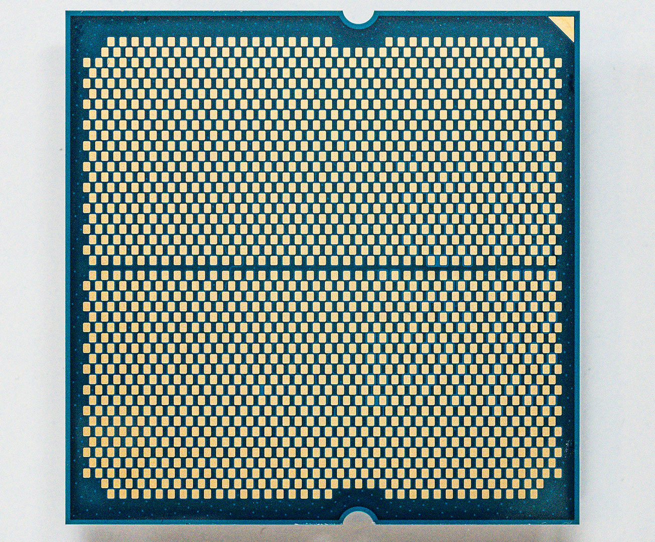
Socket AM5
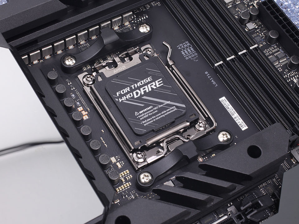
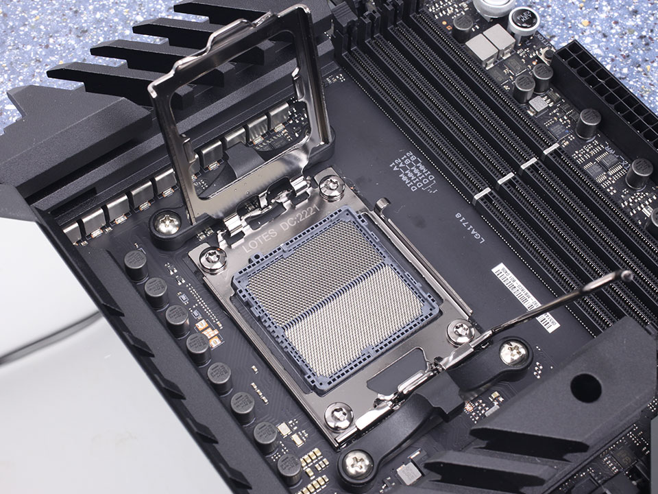
Here are a few pictures of Socket AM5, the star-attraction with this platform. This is a land-grid array (LGA) socket with 1,718 pins.
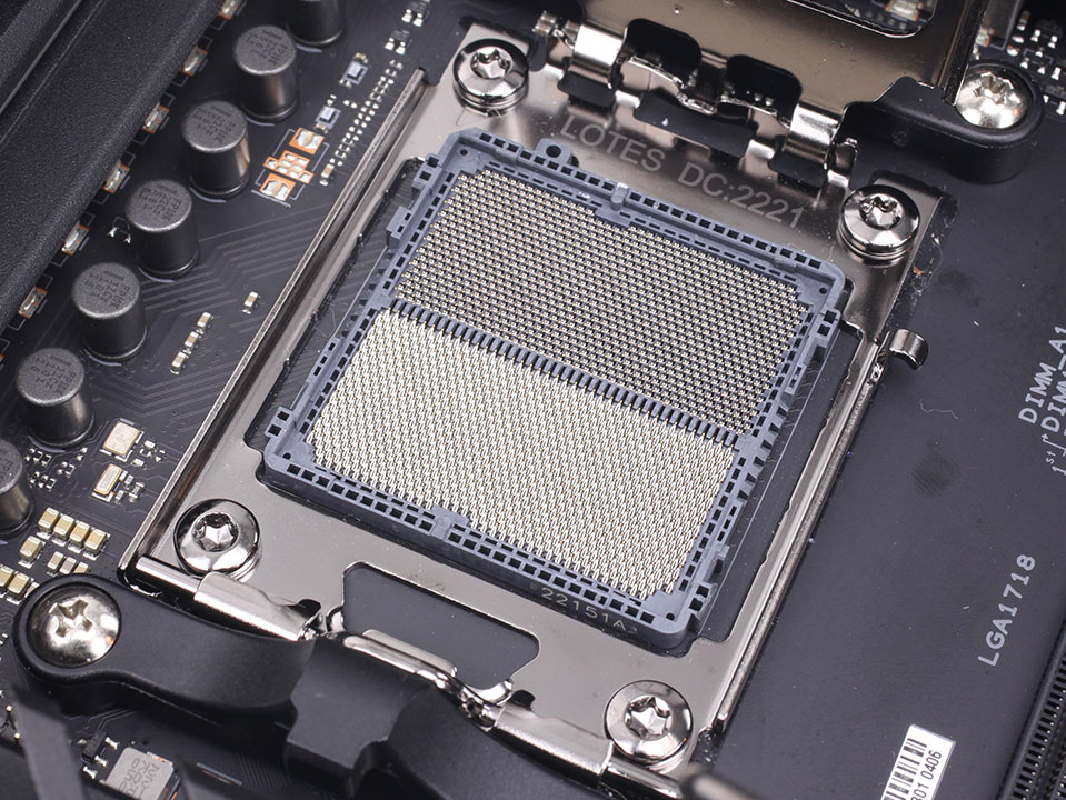
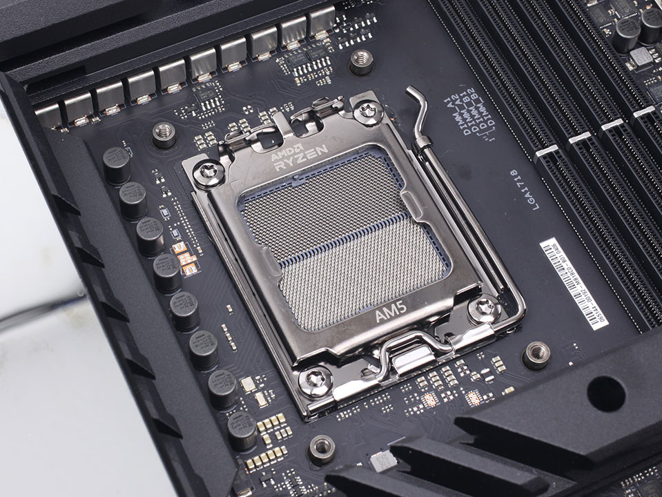
As with every LGA socket, the pins are on the motherboard, whereas the processor package has contacts that interface with those pins, while a retention brace holds the package in place with a locking lever. Installing a processor on AM5 is similar to doing so on any of the dozens of Intel LGA sockets.
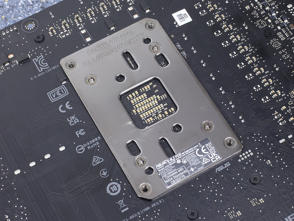
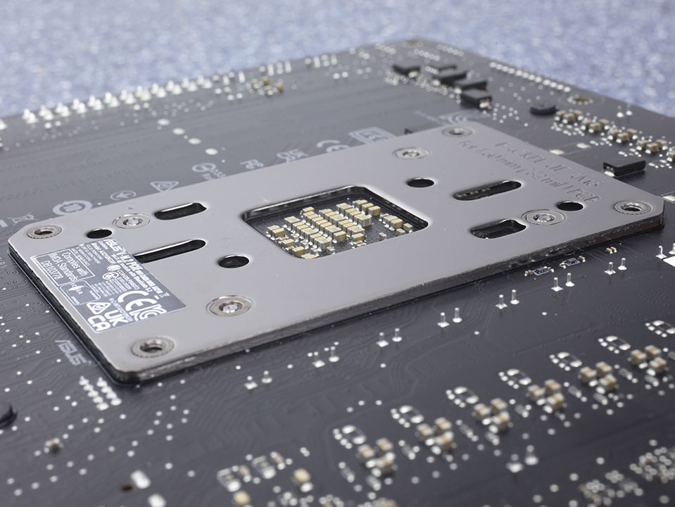
On Socket AM4, removing the four mounting screws resulted in the backplate falling off, which meant you needed three hands when installing a cooler, and several vendors also bundled their own backplates. On Socket AM5 the backplate isn't designed to be removed, which makes cooler installation MUCH easier.
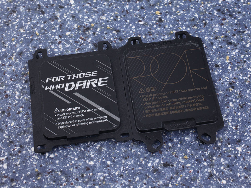
The caps for the socket are not identical to the Intel LGA sockets, so you can't reuse them.
Unboxing and Photography
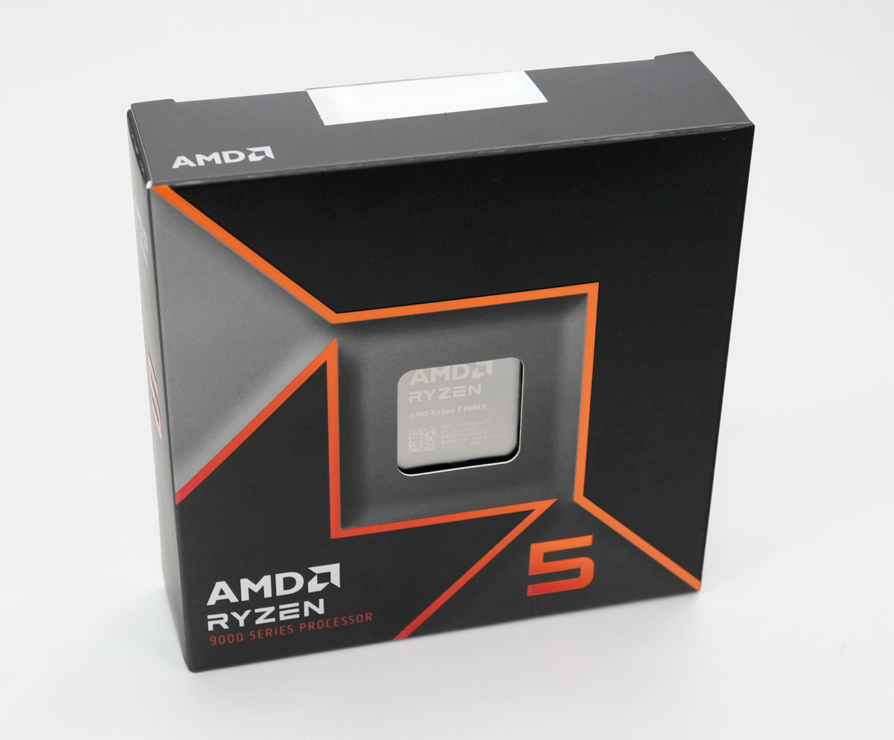
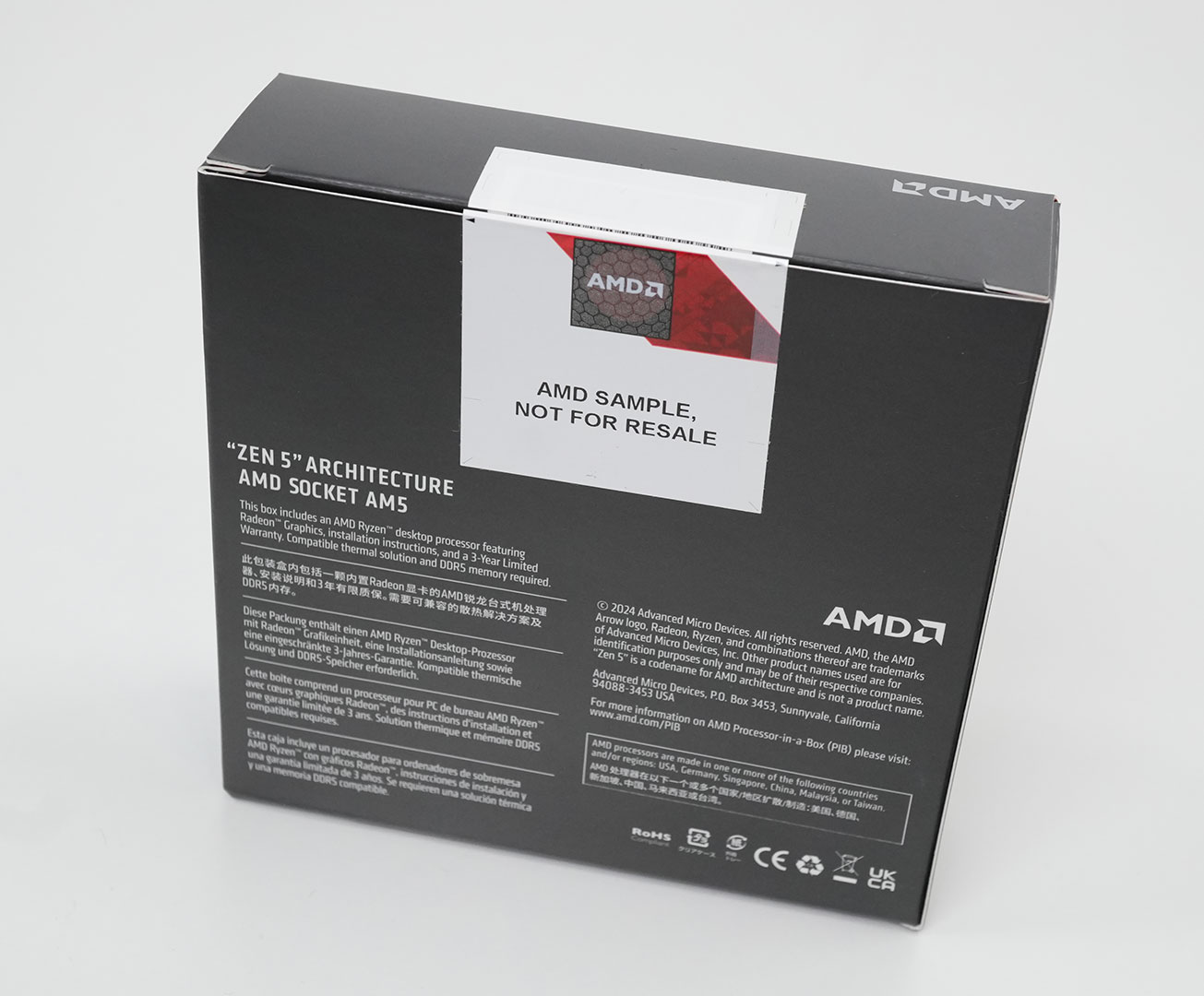
The Ryzen 5 9600X ships in a package that looks similar in box design to the Ryzen 7000 series. Unlike some Ryzen 8000 CPUs, the box doesn't scream support for Ryzen AI, since the chip lacks an NPU.
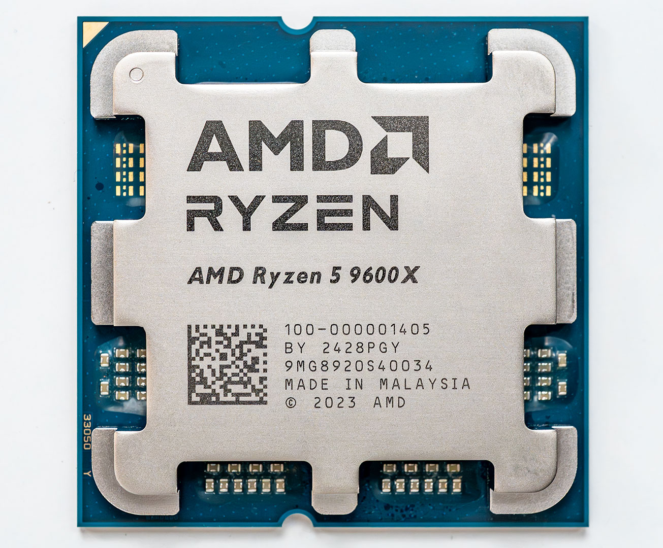
The new Ryzen 9000 Series looks just like the previous Ryzen 7000 Socket AM5 processors. While there are some minimal changes to the SMD capacitor layout, these aren't significant in any way.
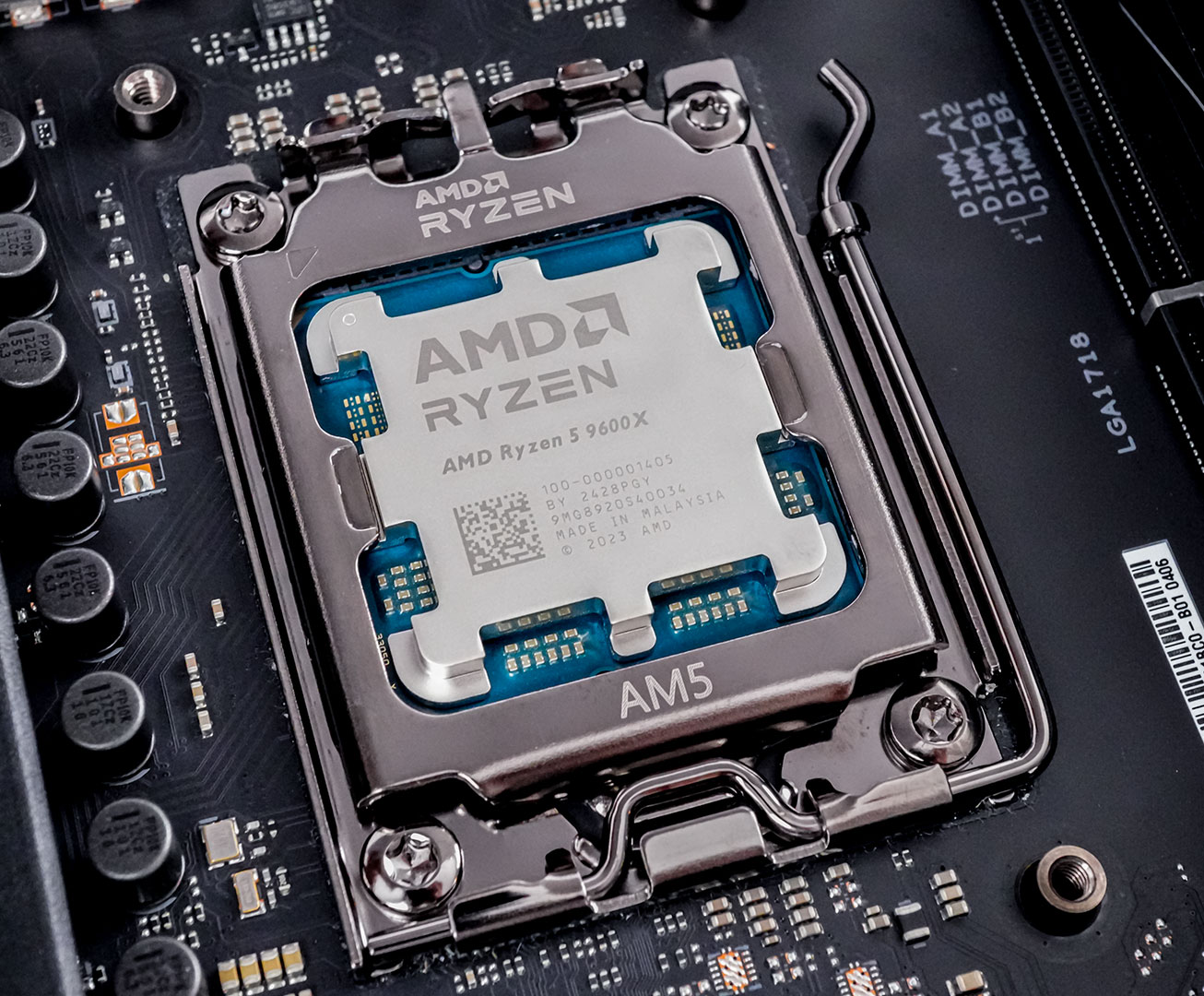
The AM5 socket retention brace only applies pressure along the two side protrusions of the IHS. Intel sockets have it the same way.
Our Patreon Silver Supporters can read articles in single-page format.
Mar 27th, 2025 21:29 EDT
change timezone
Latest GPU Drivers
New Forum Posts
- vram usage set (1)
- tape v hard disk (18)
- How to quickly & easily fix coil-whine(coil choke noise) (1138)
- Gigabyte graphic card - TIM GEL application failure? (6)
- The TPU UK Clubhouse (25981)
- TPU's Nostalgic Hardware Club (20132)
- Fun with SBCs (7)
- Future-proofing my OLED (28)
- 9070 XT - 2x HDMI high refresh displays (144 and 120 Hz) not working (68)
- Your PC ATM (35293)
Popular Reviews
- Sapphire Radeon RX 9070 XT Pulse Review
- Samsung 9100 Pro 2 TB Review - The Best Gen 5 SSD
- Assassin's Creed Shadows Performance Benchmark Review - 30 GPUs Compared
- Pulsar Feinmann F01 Review
- ASRock Phantom Gaming B860I Lightning Wi-Fi Review
- be quiet! Pure Rock Pro 3 Black Review
- Sapphire Radeon RX 9070 XT Nitro+ Review - Beating NVIDIA
- ASRock Radeon RX 9070 XT Taichi OC Review - Excellent Cooling
- ASUS ProArt X870E-Creator Wi-Fi Review
- Montech XR Wood Review
Controversial News Posts
- AMD RDNA 4 and Radeon RX 9070 Series Unveiled: $549 & $599 (260)
- MSI Doesn't Plan Radeon RX 9000 Series GPUs, Skips AMD RDNA 4 Generation Entirely (142)
- Microsoft Introduces Copilot for Gaming (123)
- AMD Radeon RX 9070 XT Reportedly Outperforms RTX 5080 Through Undervolting (118)
- NVIDIA Reportedly Prepares GeForce RTX 5060 and RTX 5060 Ti Unveil Tomorrow (115)
- Over 200,000 Sold Radeon RX 9070 and RX 9070 XT GPUs? AMD Says No Number was Given (100)
- NVIDIA GeForce RTX 5050, RTX 5060, and RTX 5060 Ti Specifications Leak (96)
- Retailers Anticipate Increased Radeon RX 9070 Series Prices, After Initial Shipments of "MSRP" Models (90)