 466
466
AMD Ryzen 7 9700X Review - The Magic of Zen 5
Socket AM5 Platform & Overclocking »Architecture
The AMD Ryzen 9000 series desktop processors, including the 9700X, 9600X, and the upcoming 9950X and 9900X, are based on the new Granite Ridge chiplet-based solution. The CPU complex dies (CCDs) are where all the innovation is focussed, as this is where the Zen 5 CPU cores are located. The rest of the processor is made up of the client I/O die (cIOD), which is carried over from the previous generation, so AMD could save on development costs. AMD built the new-generation CCD on the 4 nm TSMC N4P foundry node, an upgrade from the 5 nm TSMC N5 node, with over 22% power improvement, and 6% transistor density improvements. The CCDs are roughly the same size as the Zen 4 CCDs, and fit in nicely with the substrate floor-plan of the Granite Ridge package.
AMD has retained the CPU core counts of its previous generation, the company continues to not be baited into a core-count war with Intel triggered by its pivot to heterogeneous multicore and tiny E-cores that it can cram many of into its client processors. The Ryzen 9 9950X is the company's flagship part for this generation, and is a 16-core/32-thread chip, with two CCDs. The 9900X is 12-core/24-thread, with two CCDs, and two cores disabled per CCD. The Ryzen 7 9700X is a single CCD part, as is the Ryzen 5 9600X, which comes with two cores disabled, while retaining the full 32 MB L3 cache on the CCD.
The Zen 5 Core
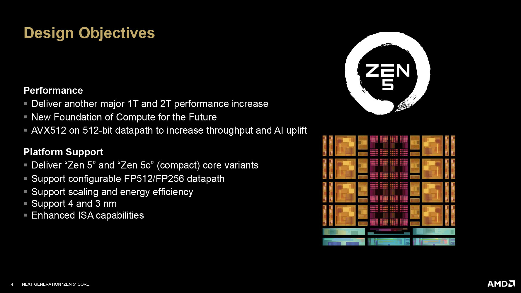
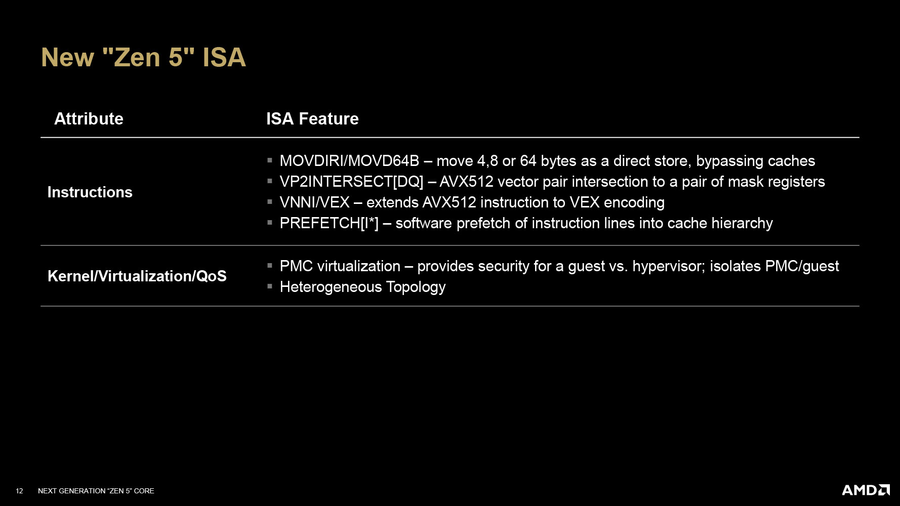
With the I/O and packaging aspects of Granite Ridge covered by carrying over the cIOD and existing Socket AM5 infrastructure, all of AMD's engineering attention is on the 4 nm CCD, and specifically, the Zen 5 CPU cores, since there's not much else on the CCD besides them. It's been AMD's endeavor to give consumers a single-thread performance improvements in the form of an IPC uplift, with each new generation of Zen. These generational IPC increases range between 10-19%, and with Zen 5, the company wants you to expect roughly 16% better IPC over Zen 4. AMD designed the Zen 5 core to be "forward-facing" with support for instruction sets that will become more relevant with the advent of AI acceleration into the client space. While the Granite Ridge processor itself lacks an NPU and won't accelerate Copilot+, the Zen 5 cores are designed to improve the working experience of AI software developers and researchers, besides machines that use discrete accelerators, since the CPU-end (software end) of the AI stack can benefit from new capabilities on the cores.
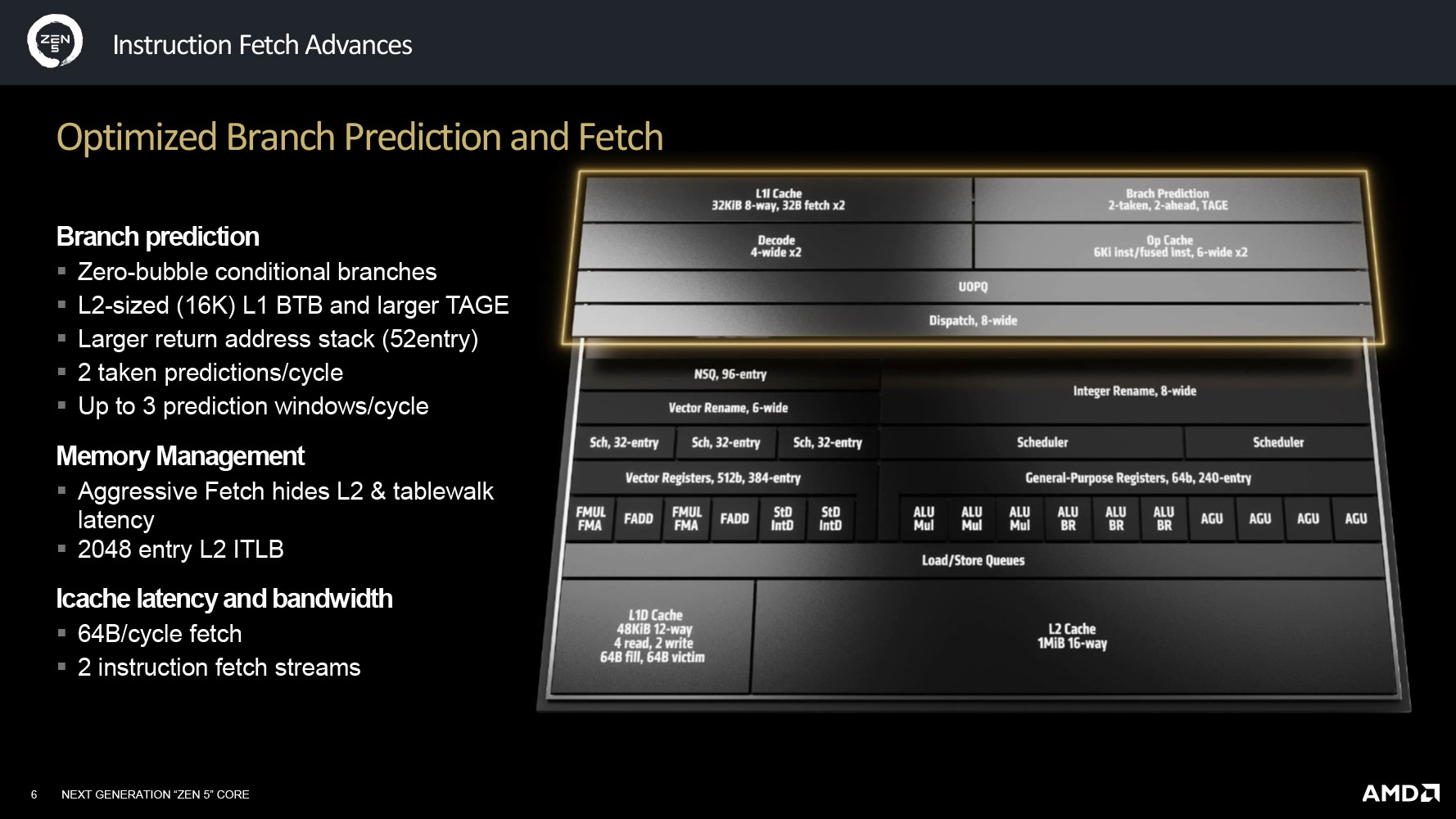
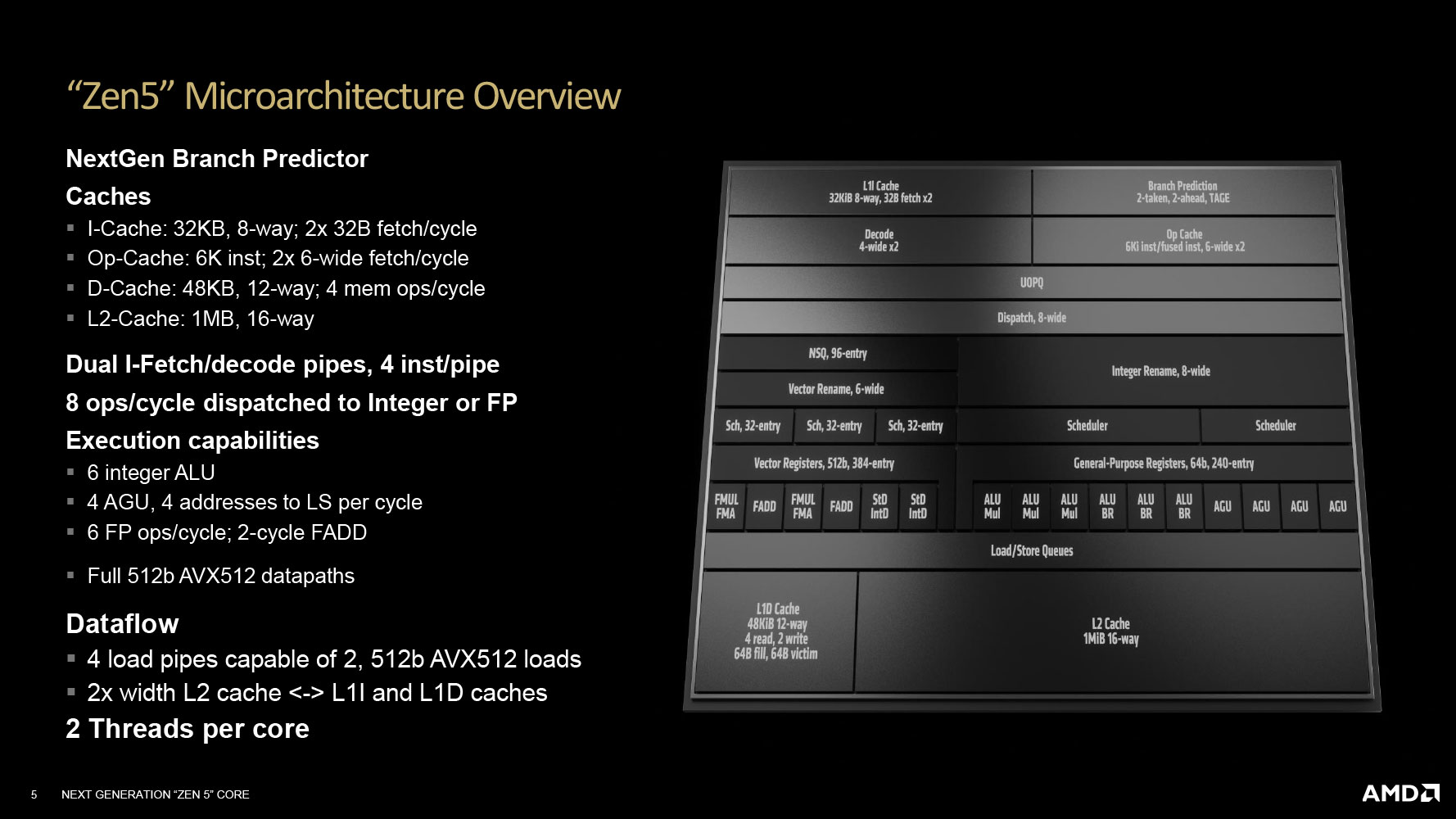
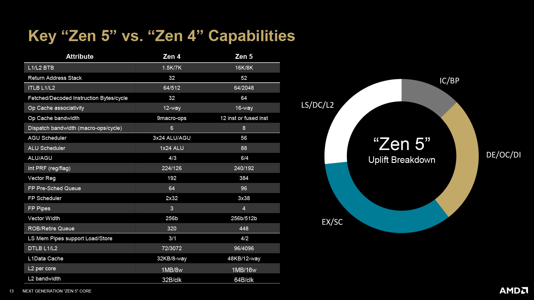
With Zen 5, AMD has updated practically all key areas of the CPU core, including the front-end with its branch prediction unit, the various caches within the core, the fetch/decode pipelines, the execution engine, and the load/store. The front-end sees an updated branch prediction unit. This new BP ensures zero-bubble conditional branches to save clock cycles from mispredictions; a large 16 KB L1 BTB, and a larger tagged-geometric length predictor; a larger 52-entry return address stack, compared to 32-entry on Zen 4; a 16-way Op Cache associativity, compared to 12-way on Zen 4, and a 33% increase in Op Cache and dispatch bandwidth. The BP supports up to 3 prediction windows per cycle, compared to 2 on Zen 4. The L2 and tablewalker latency is obscured with the new aggressive fetch unit. The L2 ITLB supports 2,048 entries, compared to just 512 on the Zen 4 core. The L1 instruction cache gets bandwidth and latency improvements, along with two independent instruction fetch streams.
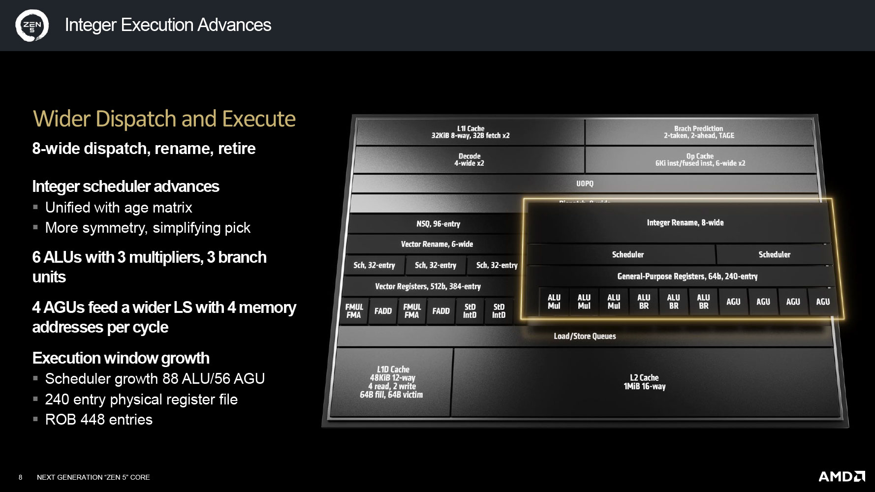
As with every traditional x86 CPU core, there's a split into Integer and Floating Point units. The Integer engine features an 8-wide dispatch/retire/rename queue depth. The integer scheduler has more "symmetry" to simplify pick operations. It features 6 ALUs with 3 multipliers, and 3 branch units; besides 4 AGUs. The AGU scheduler supports 56 entries, and the ALU scheduler 88, compared to 3x 24-entry ALU+AGU combined scheduling, with a 24-entry dedicated ALU scheduler. The physical register file is up to 240/192 entries from 224/126 on Zen 4. The ROB retire queue buffer holds 448 entries, compared to 320 on Zen 4.
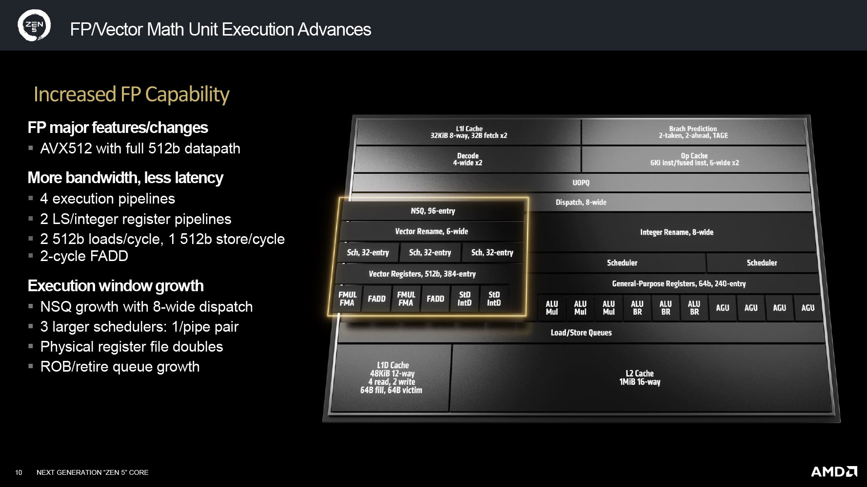
The floating point unit is where Zen 5 seems to have a major design focus. Zen 5 is designed to execute AVX-512 instructions over a full 512-bit data-path, compared to Zen 4, which uses a dual-pumped 256-bit data-path. This should significantly speed up AVX-512, VNNI, and other instructions relevant to AI acceleration on the CPU core. The FPU has four execution pipelines with two LS/integer register pipes. It supports two 512-bit loads, and one 512-bit store per cycle, and a 2-cycle FADD. There are updates to the FPU's execution window.
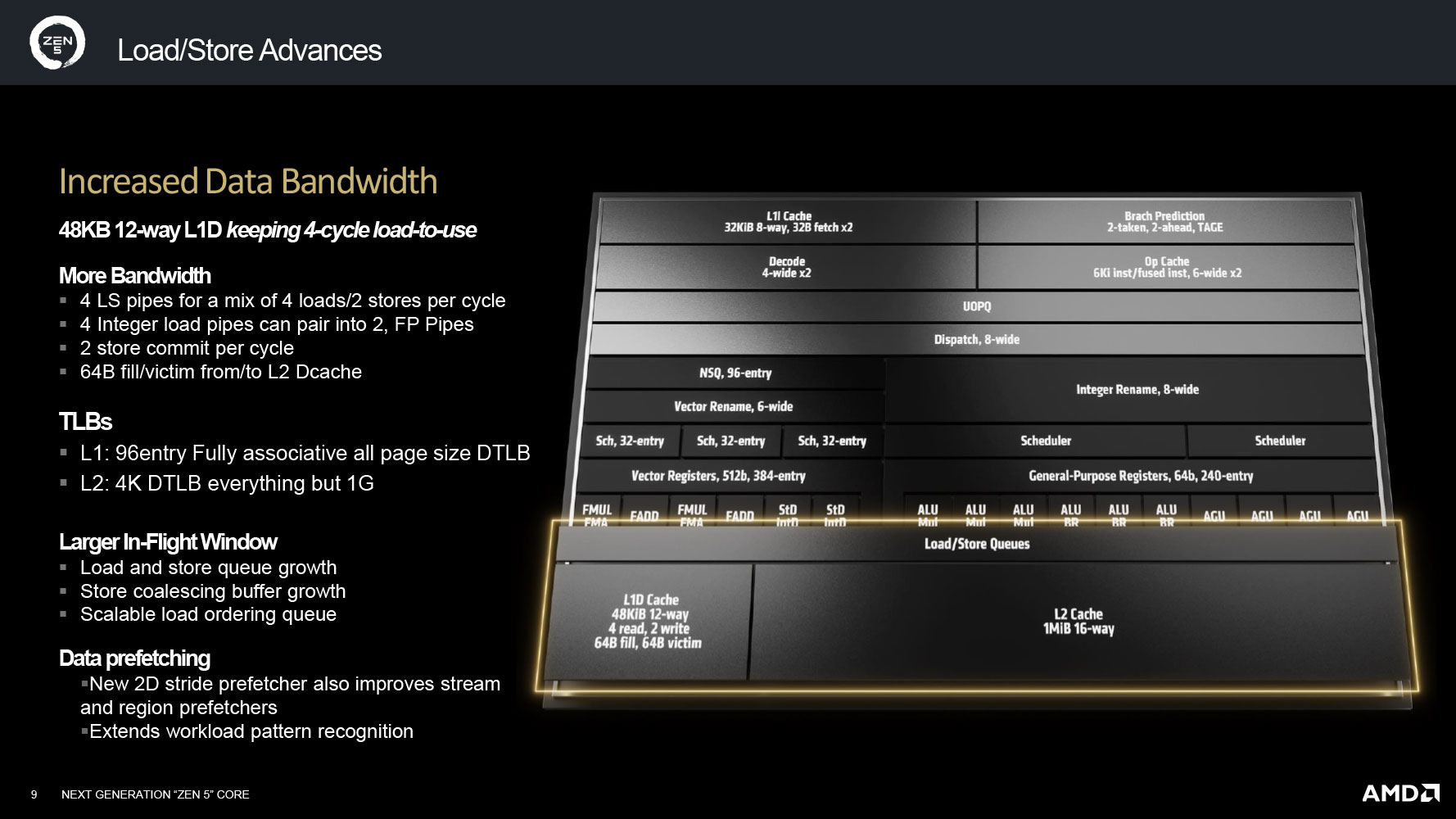
The load/store unit sees several improvements to meet the growth in bandwidth requirements of the execution engine. To begin with, the L1 data cache has been enlarged to 48 KB 12-way, up from 32 KB 8-way on Zen 4. Besides this enlargement, there are improvements to the load/store pipes, with a mix of 4 loads and 2 stores per cycle. Its four integer load pipes can pair into FP pipe. The bandwidth to the L2 cache has been improved.
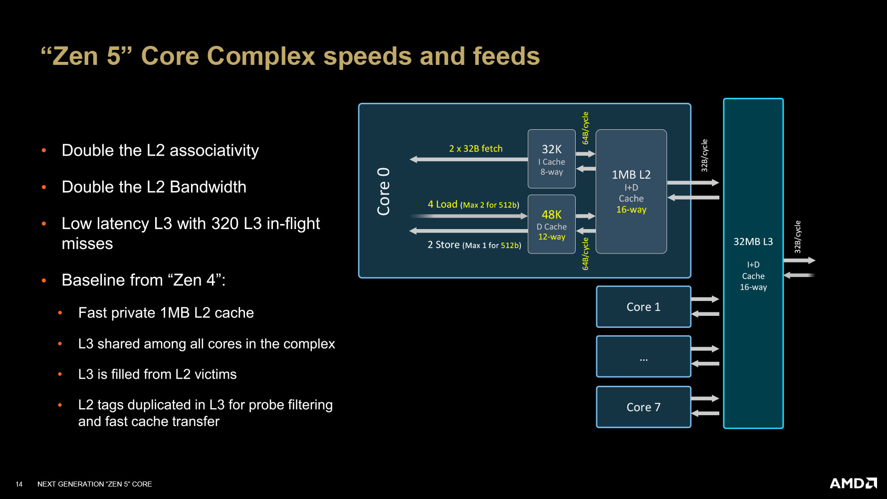
The core's dedicated L2 cache remains 1 MB in size from the previous generation, but AMD says that it has doubled the associativity and bandwidth of this cache over the one Zen 4 comes with. While AMD has retained 32 MB as the standard on-die L3 cache size, which it shares among the 8 cores on the CCD, it has worked to reduce the cache's latency along with tracking up to 320 L3 in-flight misses.
Granite Ridge SoC Features
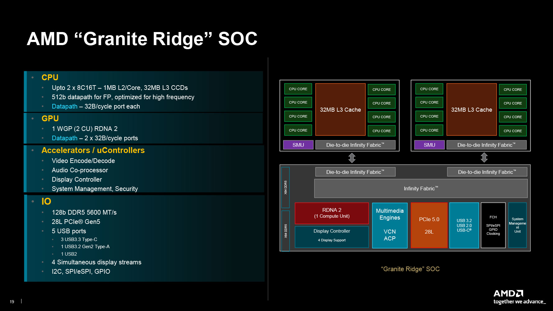
Depending on the processor model, the chip features one or two CCDs, each with 8 Zen 5 cores, 32 MB of L3 cache, an SMU, and an Infinity Fabric interface, with 32 B/cycle read and 16 B/cycle write bandwidth, to the client I/O die (cIOD). The cIOD uses Infinity Fabric to connect all the various SoC components of the processor, the two most important of which are the dual-channel DDR5 memory controllers (160-bit including ECC), and the 28-lane PCI-Express 5.0 root complex.
AMD provides a basic iGPU with Granite Ridge, just like it did with Raphael. This is based on the older RDNA 2 graphics architecture due to reusing the cIOD from Zen 4, and consists of just one workgroup processor (WGP), or just two compute units (CU), worth 128 stream processors. This iGPU talks to a display controller that supports up to four displays; and a multimedia engine that can accelerate decode of H.265 and AV1.
There's also an integrated USB interface, with support for USB 3.2 (up to two 10 Gbps ports), a couple of USB 2.0 ports, and legacy interfaces, including SPI, eSPI, GPIO, I2C, etc. The client I/O die is built on the 6 nm foundry node, as many of these components don't really benefit from the latest 4 nm node. The cIOD of Granite Ridge is carried over from Raphael, with only some microcode updates that give it native support for DDR5-5600 (Ryzen 7000 natively supported DDR5-5200), various overclocking speeds over AMD EXPO, and support for higher DDR5 overclocking memory speeds using a 1:2 divider between the FCLK and MCLK.
Mar 25th, 2025 20:18 EDT
change timezone
Latest GPU Drivers
New Forum Posts
- Build complete! Any thoughts on undervolting? (8)
- Windows 11 General Discussion (5901)
- Discussion: linux-6.14.X (3)
- Did Nvidia purposely gimp the performance of 50xx series cards with drivers (41)
- RX 9070 availability (233)
- maxsun rx590* vbios (10)
- NVCleanstall and adding hardware support (3)
- Hotspot 110° (8)
- Biostar RX 6700 XT OC BIOS (10)
- Has anyone tried enabling FSR 4 on NVIDIA cards? (2)
Popular Reviews
- Assassin's Creed Shadows Performance Benchmark Review - 30 GPUs Compared
- be quiet! Pure Rock Pro 3 Black Review
- ASUS ProArt X870E-Creator Wi-Fi Review
- ASRock Radeon RX 9070 XT Taichi OC Review - Excellent Cooling
- Sapphire Radeon RX 9070 XT Nitro+ Review - Beating NVIDIA
- Pulsar Feinmann F01 Review
- ASUS GeForce RTX 5070 TUF OC Review
- AMD Ryzen 9 9950X3D Review - Great for Gaming and Productivity
- AMD Ryzen 7 9800X3D Review - The Best Gaming Processor
- Montech XR Wood Review
Controversial News Posts
- AMD RDNA 4 and Radeon RX 9070 Series Unveiled: $549 & $599 (260)
- AMD Radeon RX 9070-series Pricing Leaks Courtesy of MicroCenter (158)
- MSI Doesn't Plan Radeon RX 9000 Series GPUs, Skips AMD RDNA 4 Generation Entirely (142)
- Microsoft Introduces Copilot for Gaming (123)
- AMD Radeon RX 9070 XT Reportedly Outperforms RTX 5080 Through Undervolting (118)
- NVIDIA Reportedly Prepares GeForce RTX 5060 and RTX 5060 Ti Unveil Tomorrow (115)
- Over 200,000 Sold Radeon RX 9070 and RX 9070 XT GPUs? AMD Says No Number was Given (100)
- NVIDIA GeForce RTX 5050, RTX 5060, and RTX 5060 Ti Specifications Leak (96)