 47
47
ASUS GeForce RTX 3080 12 GB STRIX OC Review - 20% more VRAM
Test Setup »High-resolution PCB Pictures
These pictures are for the convenience of volt modders and people who would like to see all the finer details on the PCB. Feel free to link back to us and use these in your articles, videos or forum posts.
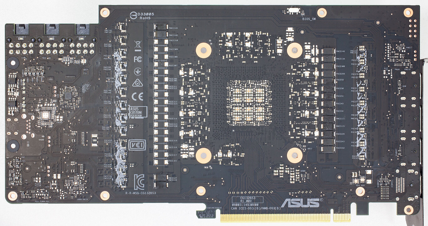
High-res versions are also available (front, back).
Circuit Board (PCB) Analysis

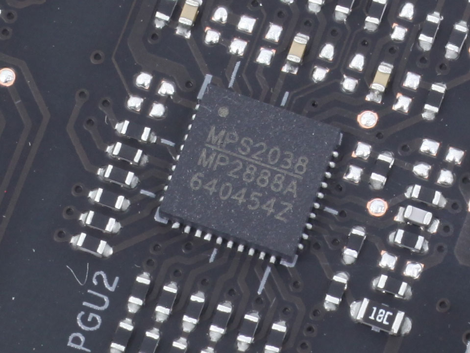

The GPU VRM is 18-phase, controlled by two Monolithic Power Systems MP2888A controllers.

For GPU voltage, Infineon TDA21570 DrMOS are used, which are rated for 70 A.


Memory voltage uses a 4-phase design and is generated by a UPI uP9628P controller

OnSemi NCP303151 DrMOS are used for memory voltage. These are capable of up to 50 A.
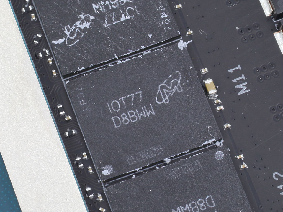
The GDDR6X memory chips are made by Micron and carry the model number D8BWW, which decodes to MT61K256M32JE-19G:T. They are specified to run at 1188 MHz (19 Gbps GDDR6X effective).
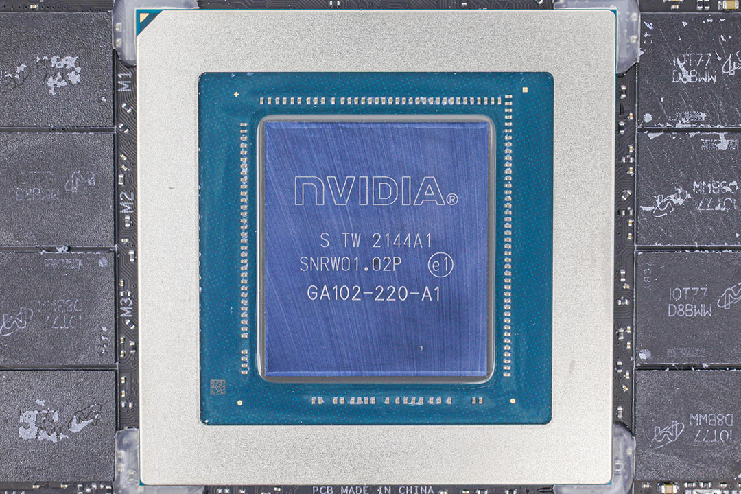
NVIDIA's GA102 graphics processor is the company's second Ampere architecture chip, the first one targeted at GeForce gamers. It is produced on a 8 nanometer process at Samsung and has a transistor count of 28 billion with a die size of 628 mm².
Mar 31st, 2025 14:48 EDT
change timezone
Latest GPU Drivers
New Forum Posts
- Help me pick a UPS (10)
- Future-proofing my OLED (90)
- Folding Pie and Milestones!! (9453)
- Do you prefer factory overclocked GPUs? (62)
- can i yust connect 4 pin cpu coler to 5 pin ? (3)
- TPU's Rosetta Milestones and Daily Pie Thread (2264)
- What do you do for a living? (462)
- Upgrade from a AMD AM3+ to AM4 or AM5 chipset MB running W10? (77)
- Help with System Recommendations (0)
- What's your latest tech purchase? (23435)
Popular Reviews
- Sapphire Radeon RX 9070 XT Pulse Review
- ASRock Phantom Gaming B850 Riptide Wi-Fi Review - Amazing Price/Performance
- Samsung 9100 Pro 2 TB Review - The Best Gen 5 SSD
- Palit GeForce RTX 5070 GamingPro OC Review
- Sapphire Radeon RX 9070 XT Nitro+ Review - Beating NVIDIA
- Assassin's Creed Shadows Performance Benchmark Review - 30 GPUs Compared
- Enermax REVOLUTION D.F. 12 850 W Review
- AMD Ryzen 7 9800X3D Review - The Best Gaming Processor
- ASRock Radeon RX 9070 XT Taichi OC Review - Excellent Cooling
- AMD Ryzen 9 9950X3D Review - Great for Gaming and Productivity
Controversial News Posts
- MSI Doesn't Plan Radeon RX 9000 Series GPUs, Skips AMD RDNA 4 Generation Entirely (142)
- Microsoft Introduces Copilot for Gaming (124)
- AMD Radeon RX 9070 XT Reportedly Outperforms RTX 5080 Through Undervolting (119)
- NVIDIA Reportedly Prepares GeForce RTX 5060 and RTX 5060 Ti Unveil Tomorrow (115)
- Over 200,000 Sold Radeon RX 9070 and RX 9070 XT GPUs? AMD Says No Number was Given (100)
- NVIDIA GeForce RTX 5050, RTX 5060, and RTX 5060 Ti Specifications Leak (96)
- Retailers Anticipate Increased Radeon RX 9070 Series Prices, After Initial Shipments of "MSRP" Models (90)
- China Develops Domestic EUV Tool, ASML Monopoly in Trouble (88)