 51
51
ASUS GeForce RTX 4060 Ti Dual with M.2 Slot Review - Gen 5 Supported
Test Setup »High-resolution PCB Pictures
These pictures are for the convenience of volt modders and people who would like to see all the finer details on the PCB. Feel free to link back to us and use these in your articles, videos or forum posts.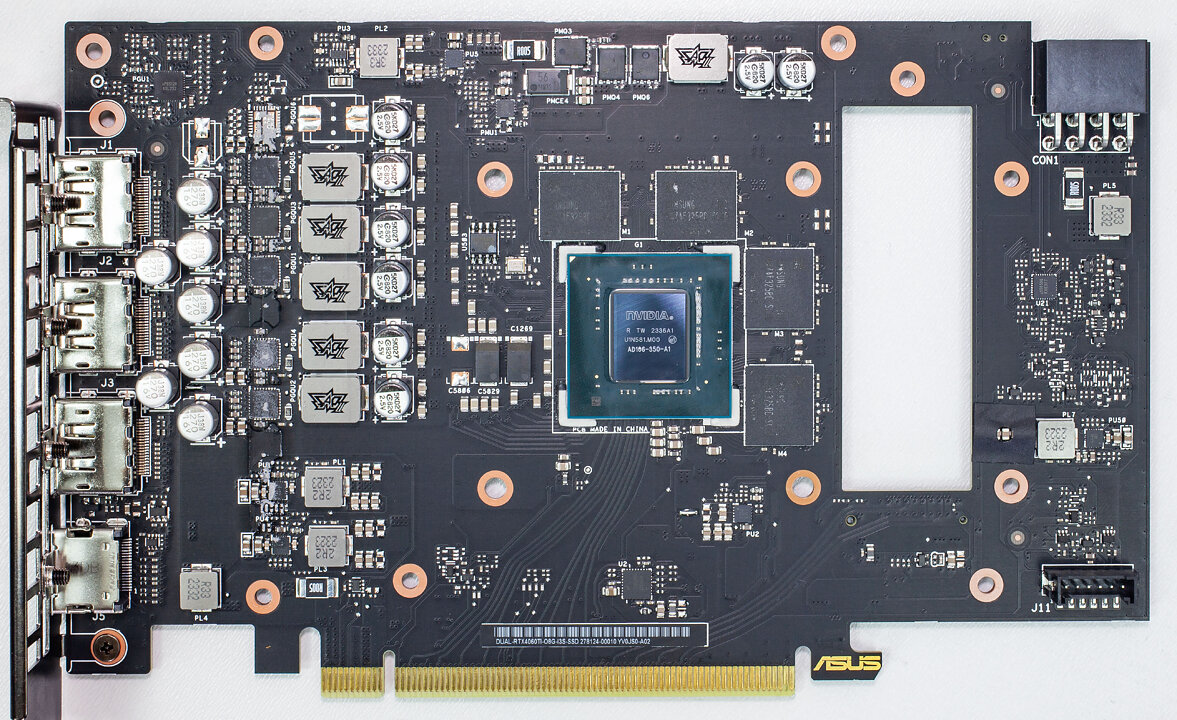
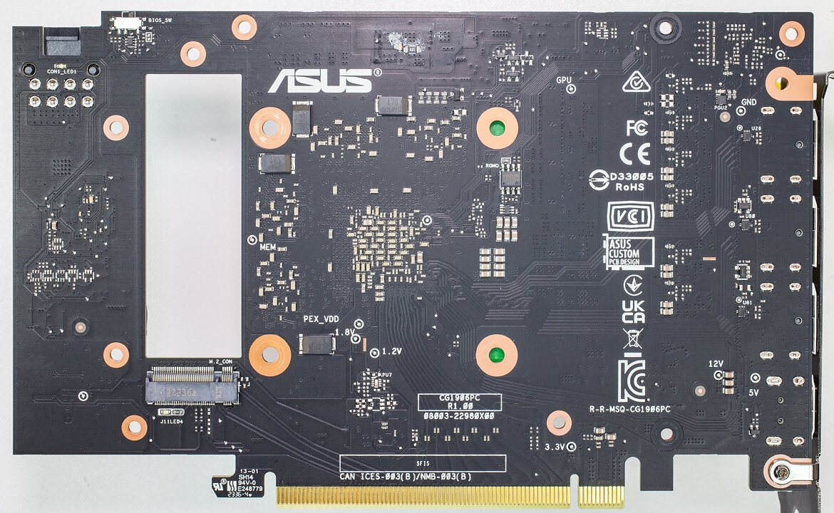
High-resolution versions are also available (front, back).
Circuit Board (PCB) Analysis
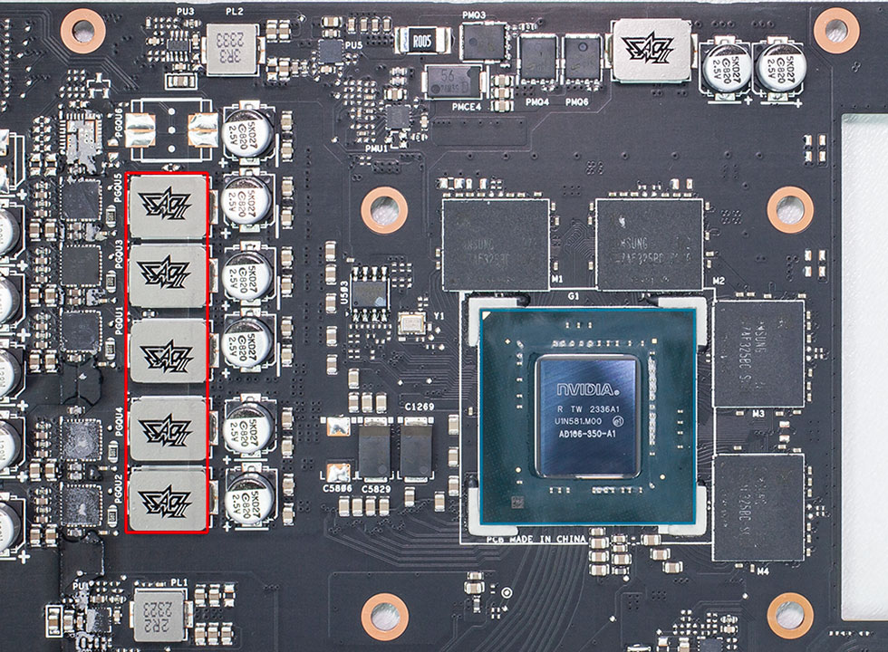
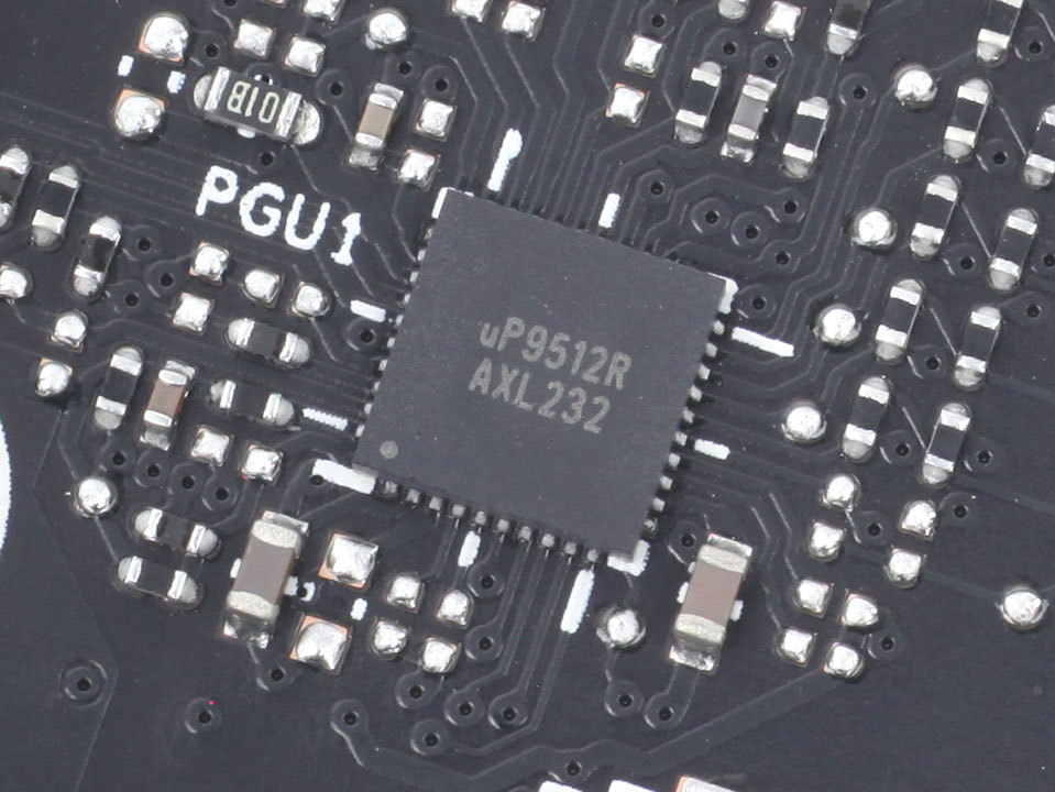
GPU voltage is a five-phase design, managed by a uPI uP9512R controller.
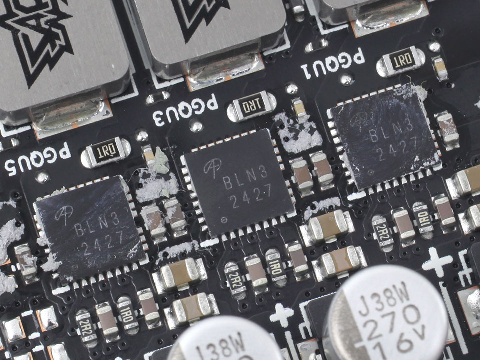
Alpha & Omega Semiconductor BLN3-AOZ5311NQI DrMOS are used for the GPU power phases, these are each capable of 55 A.
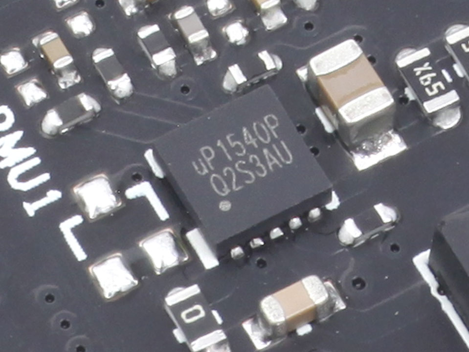
Memory voltage is a single-phase design, and handled by a UPI uP1540P controller.
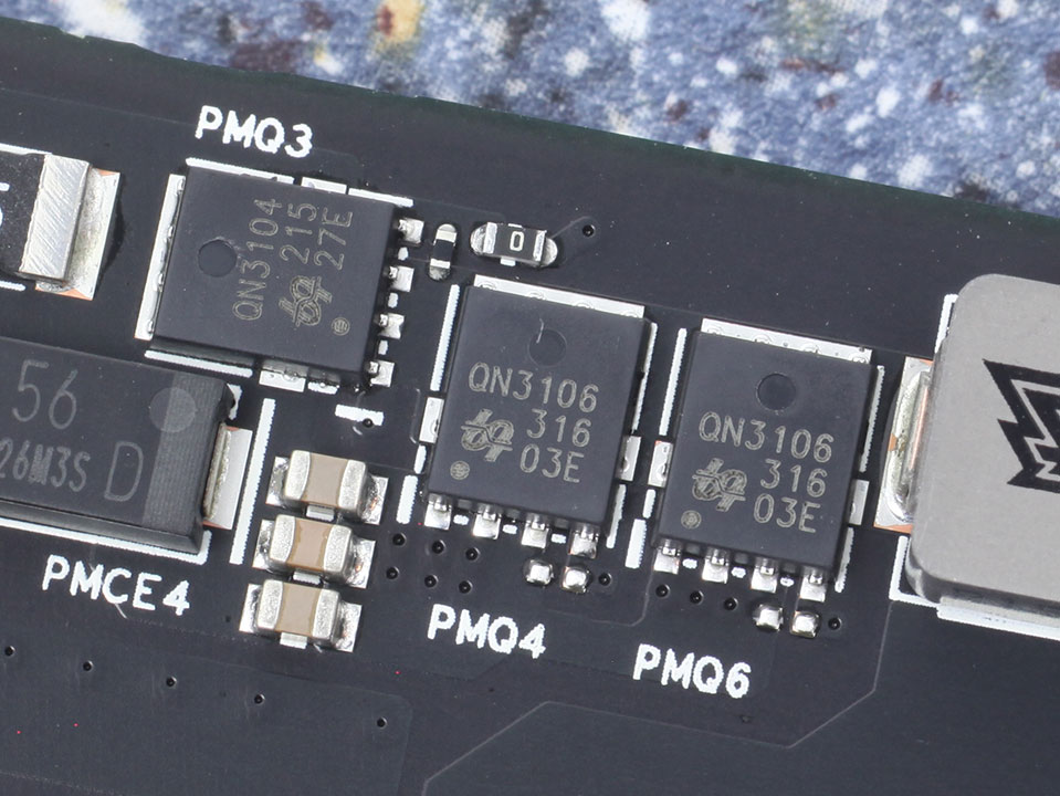
For memory, ASUS is using a set of Sinotech QN3106 and QN3104 discrete MOSFETs rated for 50 A.
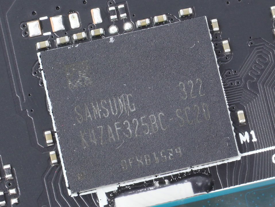
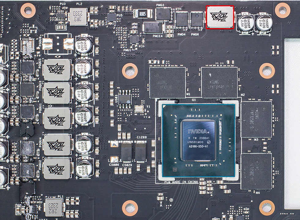
The GDDR6 memory chips are made by Samsung and carry the model number K4ZAF325BC-SC20. They are specified to run at 2500 MHz (20 Gbps effective).
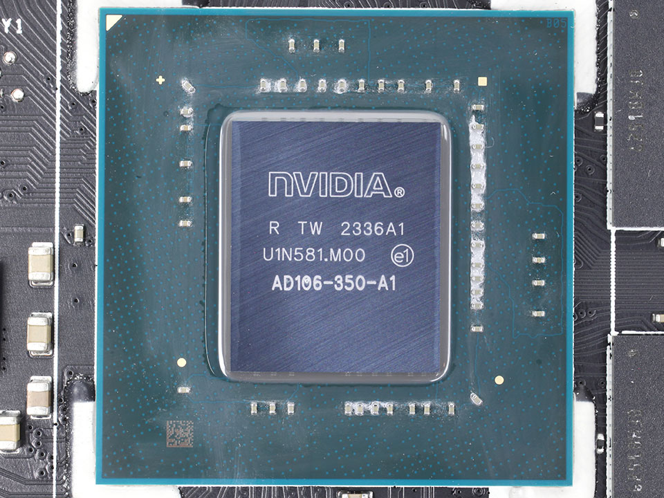
NVIDIA's AD106 graphics processor is the company's fourth Ada Lovelace GPU. It is built using a 5 nanometer process at TSMC Taiwan, with a transistor count of 22.9 billion and a die size of 190 mm².
Mar 3rd, 2025 01:11 EST
change timezone
Latest GPU Drivers
New Forum Posts
- buying oled monitor - need your advice (1)
- Trying to run 4k 144hz using 3070ti (9)
- Cooling problems persist on LGA1700 (19)
- RTX5000 Series Owners Club (143)
- Found a weird Radeon HD 7950 with 1536 shaders and no temperature readout (17)
- It's happening again, melting 12v high pwr connectors (988)
- Throttle stop and M18R2 (7)
- Windows 11 General Discussion (5757)
- ROCm OS? (8)
- What local LLM-s you use? (93)
Popular Reviews
- AMD Radeon RX 9070 Series Technical Deep Dive
- be quiet! Pure Base 501 DX Review
- ASUS GeForce RTX 5070 Ti TUF OC Review
- AMD Ryzen 7 9800X3D Review - The Best Gaming Processor
- MSI GeForce RTX 5070 Ti Vanguard SOC Review
- ASUS ROG Harpe Ace Mini Review
- MSI GeForce RTX 5070 Ti Ventus 3X OC Review
- Gigabyte X870 Aorus Elite WiFi 7 Review
- KLEVV CRAS C930 2 TB Review
- MSI GeForce RTX 5070 Ti Gaming Trio OC+ Review
Controversial News Posts
- NVIDIA GeForce RTX 50 Cards Spotted with Missing ROPs, NVIDIA Confirms the Issue, Multiple Vendors Affected (509)
- AMD Plans Aggressive Price Competition with Radeon RX 9000 Series (274)
- AMD Radeon RX 9070 and 9070 XT Listed On Amazon - One Buyer Snags a Unit (257)
- AMD Mentions Sub-$700 Pricing for Radeon RX 9070 GPU Series, Looks Like NV Minus $50 Again (248)
- NVIDIA Investigates GeForce RTX 50 Series "Blackwell" Black Screen and BSOD Issues (244)
- AMD RDNA 4 and Radeon RX 9070 Series Unveiled: $549 & $599 (225)
- AMD Radeon RX 9070 and 9070 XT Official Performance Metrics Leaked, +42% 4K Performance Over Radeon RX 7900 GRE (192)
- AMD Radeon RX 9070-series Pricing Leaks Courtesy of MicroCenter (156)