 51
51
ASUS GeForce RTX 4060 Ti Dual with M.2 Slot Review - Gen 5 Supported
(51 Comments) »Introduction
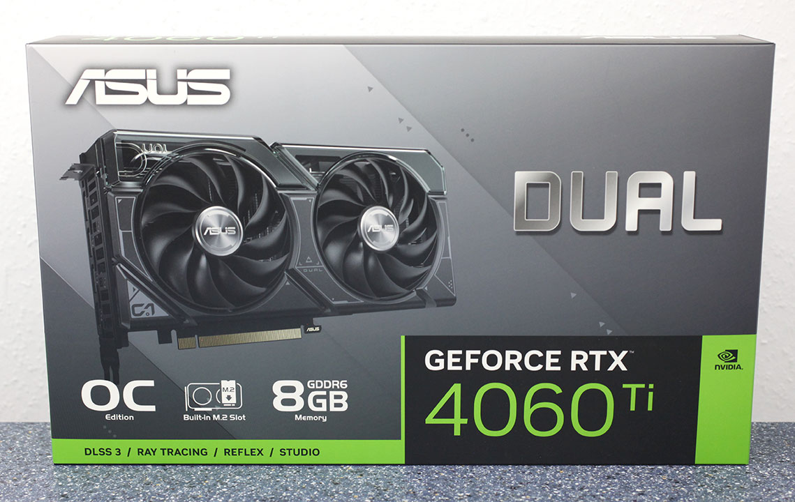
Here's a kind of graphics card we've always wanted to see—the ASUS GeForce RTX 4060 Ti Dual with an M.2 Slot is a unique contraption that combines a graphics card with an M.2 NVMe SSD slot. The card features an M.2-2280 slot with full PCI-Express 5.0 x4 wiring that pulls the unused lanes from the card's main PCIe interface, without any bridge or lane switches in between. The result is a fully-featured RTX 4060 Ti graphics card with uncompromised performance, plus the ability to put some unused PCIe lanes to use.
NVIDIA designed the RTX 4060 Ti GPU with a PCI-Express 4.0 x8 host interface. When installed in a motherboard with a full x16 PCIe slot, this results in 8 unused PCIe lanes, unless the motherboard is able to divert those lanes to a second x16 slot, or an M.2 NVMe slot of its own (as is the case with all Socket LGA1700 motherboards that feature a Gen 5 M.2 slot). This card has its first 8 lanes wired to the GPU, and the following 4 lanes wired to an M.2-2280 slot. For this to work, the motherboard must support PCIe lane segmentation, also known as "bifurcation."

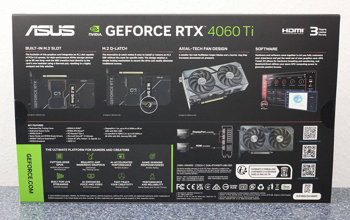
There are a couple of advantages to this card's M.2 slot. For starters, the M.2 slot features Gen 5 wiring, so when installed on a platform with a PCI-Express 5.0 x16 slot, you get a ready-to-use Gen 5 NVMe slot; and second, this M.2 slot is guaranteed to be wired to the processor's PCIe root complex, and not the chipset, so it should offer the highest possible performance. This card paves the way for other such innovative products in the near future such as, say, a graphics card with a PCIe x8 GPU and a Thunderbolt or USB4 controller that puts out a swanky 40 Gbps port with internal DisplayPort wiring from the GPU—the possibilities are endless when engineers are given a free hand!
The main function of this card is still that of a gaming graphics card, and the GeForce RTX 4060 Ti Ada occupies an important price point in NVIDIA's product stack. It is designed for maxed out gaming at 1440p and 1080p resolutions, and since it's based on the latest Ada Lovelace graphics architecture, you get all of NVIDIA's latest features, including DLSS 3 Frame Generation. With this family of GPUs, NVIDIA has switched over to TSMC's 5 nm EUV foundry node, which gives you next generation energy efficiency—the card only needs a single 8-pin PCIe power input to power the GPU.
The Ada Lovelace graphics architecture sees NVIDIA's third generation of RTX, a breakthrough combination of gaming technologies that bring real time ray tracing to gamers; and performance improvements with DLSS. The new "Ada" CUDA core, in addition to increased IPC and support for new math formats, comes with support for shader execution re-ordering, which should benefit ray tracing workloads. The 3rd generation RT core, besides generational improvements to the ray intersection performance, adds support displaced micro-meshes, which increases the complexity of ray traced objects. The new Optical Flow Accelerator component assists in the generation of entire alternate frames entirely using AI, which is why DLSS 3 Frame Generation is exclusive to the RTX 40-series.
The GeForce RTX 4060 Ti nearly maxes out the AD106 silicon it's based on, by enabling 34 out of 36 streaming multiprocessors physically present on the silicon. This works out to 4,352 CUDA cores, 136 Tensor cores, 34 RT cores, 136 TMUs, and 48 ROPs. The card's 8 GB GDDR6 memory is installed across a seemingly narrow 128-bit memory interface, which is generationally halved from the 256-bit bus of the RTX 3060 Ti Ampere; but don't fret—NVIDIA re-architected the memory sub-system with Ada to place greater dependence on large on-die caches, which should speed up the memory transfers.
Besides the M.2 NVMe slot, this card is practically identical in design to the ASUS RTX 4060 Ti Dual, the company's affordable custom-design implementation of the GPU that's positioned a notch below its TUF Gaming and ROG Strix RTX 4060 Ti cards. ASUS including a small factory overclock to a rated boost clock of 2565 MHz. The company is pricing the card at a $40 or a 10% premium over the $400 baseline price of the RTX 4060 Ti 8 GB, which should put it pretty close to the RTX 4060 Ti 16 GB variant that sells for $450. In this review, not only are we testing the card's main GPU chops, but also the performance of its M.2 NVMe slot using popular Gen 4 and Gen 5 SSDs. We will be comparing SSD performance against various placement options on the motherboard, as well as an M.2 add-in-card card that sits on the motherboard's second x16 slot, with lane switches along the way.
| Price | Cores | ROPs | Core Clock | Boost Clock | Memory Clock | GPU | Transistors | Memory | |
|---|---|---|---|---|---|---|---|---|---|
| Arc A750 | $200 | 3584 | 112 | 2050 MHz | N/A | 2000 MHz | ACM-G10 | 21700M | 8 GB, GDDR6, 256-bit |
| RX 6600 | $170 | 1792 | 64 | 2044 MHz | 2491 MHz | 1750 MHz | Navi 23 | 11060M | 8 GB, GDDR6, 128-bit |
| RX 6600 XT | $200 | 2048 | 64 | 2359 MHz | 2589 MHz | 2000 MHz | Navi 23 | 11060M | 8 GB, GDDR6, 128-bit |
| RTX 3060 | $240 | 3584 | 48 | 1320 MHz | 1777 MHz | 1875 MHz | GA106 | 12000M | 12 GB, GDDR6, 192-bit |
| RX 7600 | $250 | 2048 | 64 | 2250 MHz | 2625 MHz | 2250 MHz | Navi 33 | 13300M | 8 GB, GDDR6, 128-bit |
| RTX 4060 | $300 | 3072 | 48 | 1830 MHz | 2460 MHz | 2125 MHz | AD107 | 18900M | 8 GB, GDDR6, 128-bit |
| Arc A770 | $280 | 4096 | 128 | 2100 MHz | N/A | 2187 MHz | ACM-G10 | 21700M | 16 GB, GDDR6, 256-bit |
| RTX 3060 Ti | $250 | 4864 | 80 | 1410 MHz | 1665 MHz | 1750 MHz | GA104 | 17400M | 8 GB, GDDR6, 256-bit |
| RTX 4060 Ti | $400 | 4352 | 48 | 2310 MHz | 2535 MHz | 2250 MHz | AD106 | 22900M | 8 GB, GDDR6, 128-bit |
| ASUS RTX 4060 Ti Dual M.2 SSD | $440 | 4352 | 48 | 2310 MHz | 2565 MHz | 2250 MHz | AD106 | 22900M | 8 GB, GDDR6, 128-bit |
| RX 6700 XT | $300 | 2560 | 64 | 2424 MHz | 2581 MHz | 2000 MHz | Navi 22 | 17200M | 12 GB, GDDR6, 192-bit |
| RTX 3070 | $310 | 5888 | 96 | 1500 MHz | 1725 MHz | 1750 MHz | GA104 | 17400M | 8 GB, GDDR6, 256-bit |
| RTX 3070 Ti | $350 | 6144 | 96 | 1575 MHz | 1770 MHz | 1188 MHz | GA104 | 17400M | 8 GB, GDDR6X, 256-bit |
| RX 6800 | $450 | 3840 | 96 | 1815 MHz | 2105 MHz | 2000 MHz | Navi 21 | 26800M | 16 GB, GDDR6, 256-bit |
| RX 7700 XT | $440 | 3456 | 96 | 2171 MHz | 2544 MHz | 2250 MHz | Navi 32 | 26500M | 12 GB, GDDR6, 192-bit |
| RX 6800 XT | $500 | 4608 | 128 | 2015 MHz | 2250 MHz | 2000 MHz | Navi 21 | 26800M | 16 GB, GDDR6, 256-bit |
| RTX 3080 | $450 | 8704 | 96 | 1440 MHz | 1710 MHz | 1188 MHz | GA102 | 28000M | 10 GB, GDDR6X, 320-bit |
| RTX 4070 | $550 | 5888 | 64 | 1920 MHz | 2475 MHz | 1313 MHz | AD104 | 35800M | 12 GB, GDDR6X, 192-bit |
| RX 7800 XT | $550 | 3840 | 96 | 2124 MHz | 2430 MHz | 2425 MHz | Navi 32 | 28100M | 16 GB, GDDR6, 256-bit |
| RX 6900 XT | $650 | 5120 | 128 | 2015 MHz | 2250 MHz | 2000 MHz | Navi 21 | 26800M | 16 GB, GDDR6, 256-bit |
Packaging
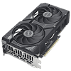
The Card

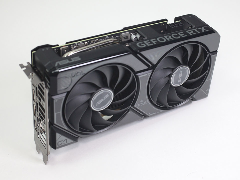
The ASUS Dual OC looks bulky and muscular. The color theme consists of black, with some gray highlights. While main cooler shroud is made of plastic, the backplate is metal.


Dimensions of the card are 23.0 x 12.5 cm, and it weighs 732 g.


Installation requires three slots in your system. The card's width is 50 mm.

Display connectivity includes three standard DisplayPort 1.4a ports and one HDMI 2.1a (same as Ampere).
The new 8th Gen NVENC now accelerates AV1 encoding, besides HEVC. You also get an "optical flow accelerator" unit that is able to calculate intermediate frames for videos, to smooth playback. The same hardware unit is used for frame generation in DLSS 3.

ASUS opted for a single 8-pin PCIe power connector, this configuration is good for up to 225 W. Right next the power input is a dual BIOS switch, which lets you switch to a secondary "quiet" BIOS, which runs at a more relaxed fan curve and stops the fan in idle. By default, the card runs with the "Performance" BIOS, which doesn't have fan stop, according to ASUS this is to ensure that even a Gen 5 M.2 SSD receives enough cooling, even when the GPU is idle.
M.2 Slot

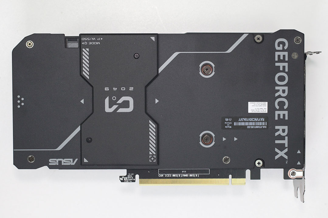
The M.2 slot sits behind a small cover that's attached with two screws.

There's a thermal pad on both sides of the slot, to maximize cooling performance.
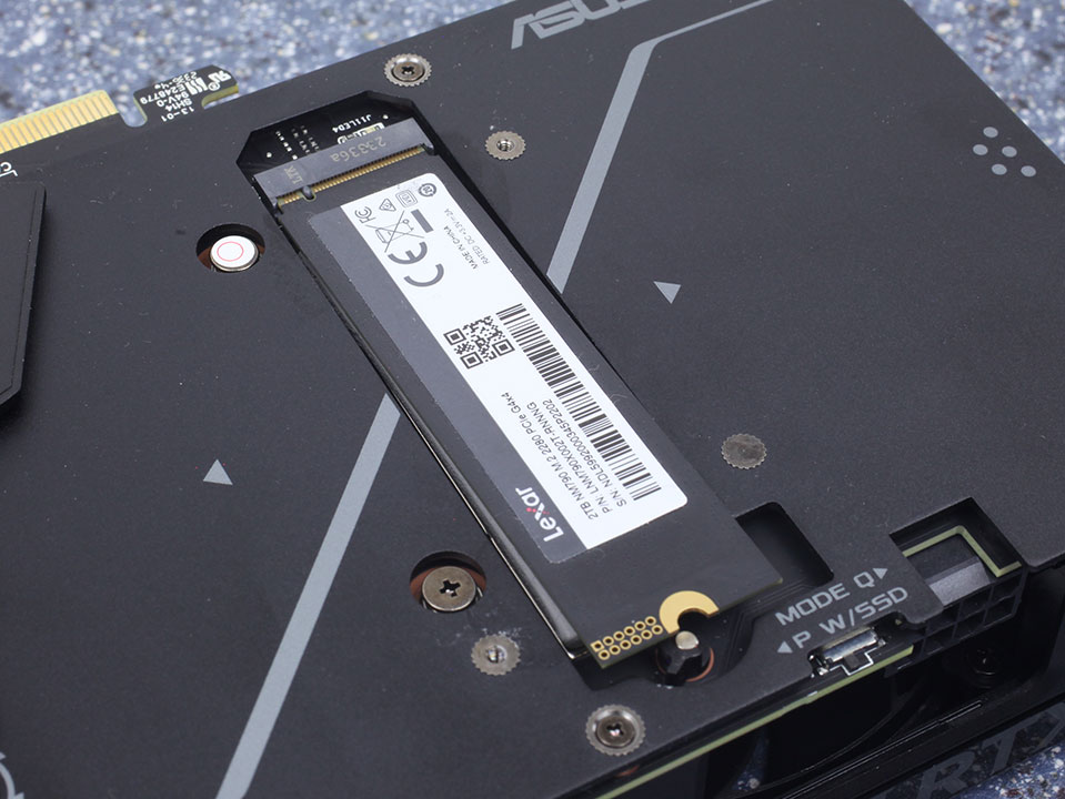
ASUS is using a "reversed" M.2 slot—the SSD doesn't face up like in your motherboard, but the other way round. This makes a lot of sense, because the GPU's main cooling solution is on the other side of the card, and with this alignment, ASUS made sure that most of the heat can be absorbed by the main cooler.

The quick-release mechanism works very well and is tool-free.
Teardown


ASUS lets you remove the main cooler shroud, so the fans can be cleaned and replaced easily, without disturbing the thermal paste on the main cooler.


The thermal solution on the ASUS Dual uses a copper base, paired with three heatpipes. The main heatsink also provides cooling for the memory chips, VRM circuitry and the M.2 SSD (note the large thermal pad).


The backplate is made of metal and protects the card against damage during installation and handling, it has a cutout for the M.2 SSD.
High-resolution PCB Pictures
These pictures are for the convenience of volt modders and people who would like to see all the finer details on the PCB. Feel free to link back to us and use these in your articles, videos or forum posts.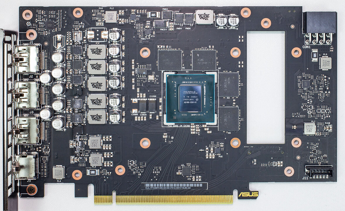
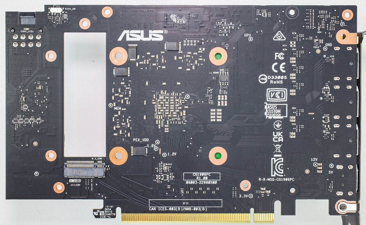
High-resolution versions are also available (front, back).
Circuit Board (PCB) Analysis
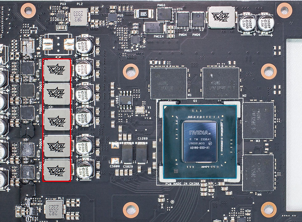
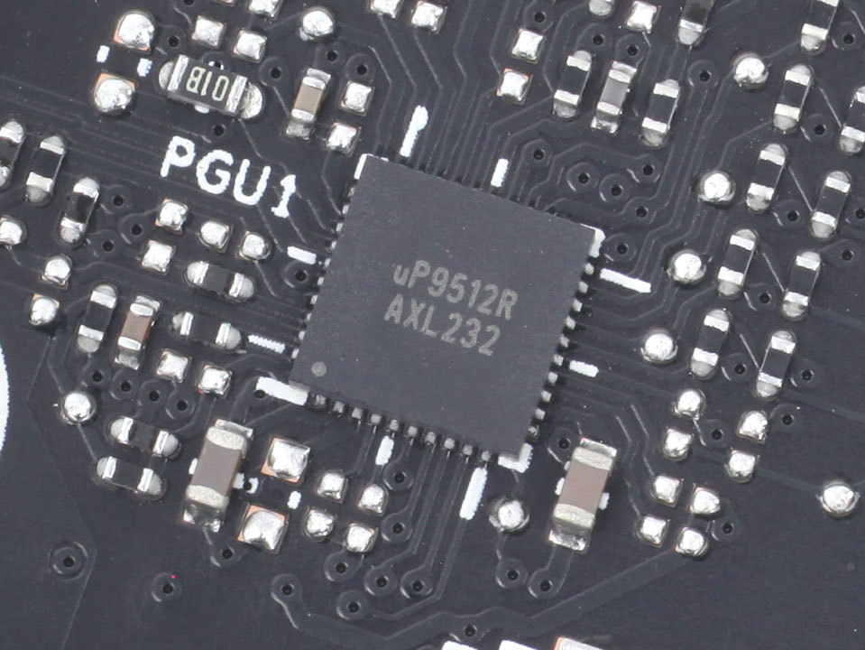
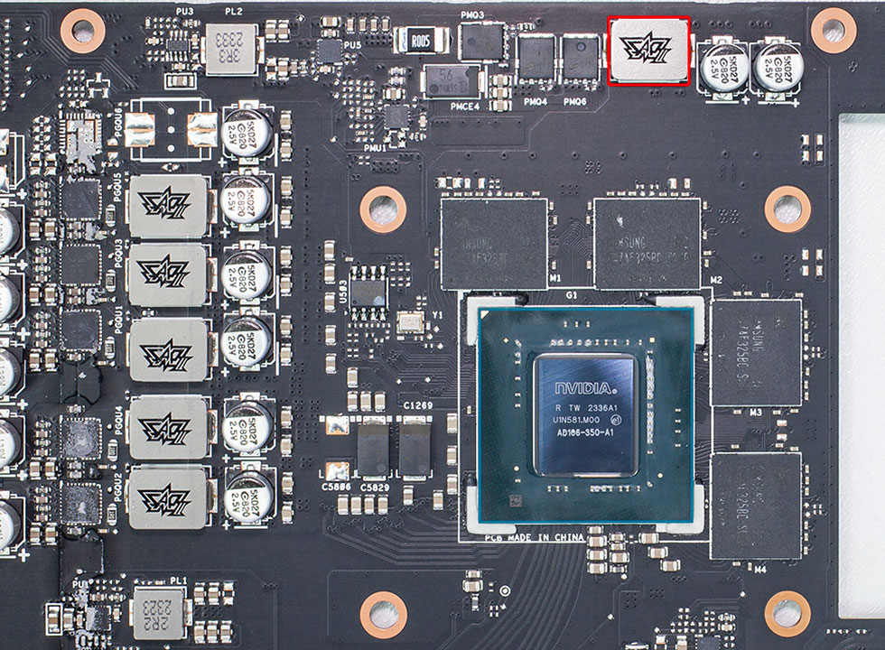
GPU voltage is a five-phase design, managed by a uPI uP9512R controller.
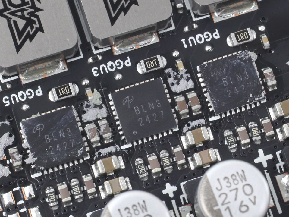
Alpha & Omega Semiconductor BLN3-AOZ5311NQI DrMOS are used for the GPU power phases, these are each capable of 55 A.
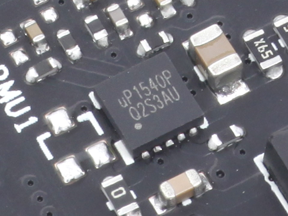
Memory voltage is a single-phase design, and handled by a UPI uP1540P controller.
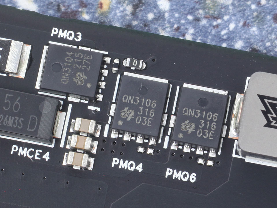
For memory, ASUS is using a set of Sinotech QN3106 and QN3104 discrete MOSFETs rated for 50 A.
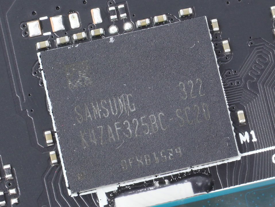
The GDDR6 memory chips are made by Samsung and carry the model number K4ZAF325BC-SC20. They are specified to run at 2500 MHz (20 Gbps effective).
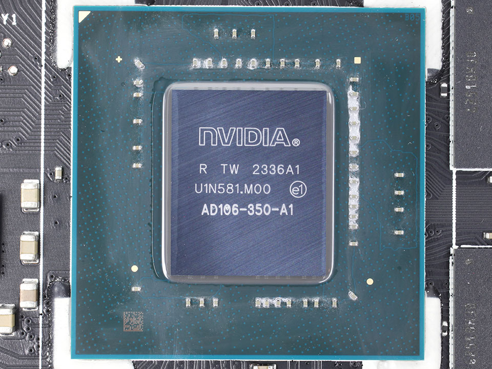
NVIDIA's AD106 graphics processor is the company's fourth Ada Lovelace GPU. It is built using a 5 nanometer process at TSMC Taiwan, with a transistor count of 22.9 billion and a die size of 190 mm².
Our Patreon Silver Supporters can read articles in single-page format.
Jul 10th, 2025 02:40 CDT
change timezone
Latest GPU Drivers
New Forum Posts
- Do you still use Antivirus software on your latest hardware? (75)
- Screen burn-in (21)
- TPU's Nostalgic Hardware Club (20493)
- 3DMARK "LEGENDARY" (326)
- Post Your TIMESPY, PCMARK10 & FIRESTRIKE SCORES! (2019) (321)
- 5070ti overclock...what are your settings? (47)
- 'NVIDIA App' not usable offline? (1)
- G-Sync Not Working in Borderless / Window Mode - Windows 11 (5)
- [GPU-Z Test Build] New Kernel Driver, Everyone: Please Test (78)
- Friend's monitor randomly loses signal (3)
Popular Reviews
- NZXT N9 X870E Review
- NVIDIA GeForce RTX 5050 8 GB Review
- Fractal Design Epoch RGB TG Review
- Corsair FRAME 5000D RS Review
- Fractal Design Scape Review - Debut Done Right
- AMD Ryzen 7 9800X3D Review - The Best Gaming Processor
- Sapphire Radeon RX 9060 XT Pulse OC 16 GB Review - An Excellent Choice
- Upcoming Hardware Launches 2025 (Updated May 2025)
- Sapphire Radeon RX 9070 XT Nitro+ Review - Beating NVIDIA
- PowerColor ALPHYN AM10 Review
TPU on YouTube
Controversial News Posts
- Intel's Core Ultra 7 265K and 265KF CPUs Dip Below $250 (288)
- Some Intel Nova Lake CPUs Rumored to Challenge AMD's 3D V-Cache in Desktop Gaming (140)
- NVIDIA Launches GeForce RTX 5050 for Desktops and Laptops, Starts at $249 (117)
- AMD Radeon RX 9070 XT Gains 9% Performance at 1440p with Latest Driver, Beats RTX 5070 Ti (116)
- NVIDIA GeForce RTX 5080 SUPER Could Feature 24 GB Memory, Increased Power Limits (115)
- Microsoft Partners with AMD for Next-gen Xbox Hardware (105)
- Intel "Nova Lake‑S" Series: Seven SKUs, Up to 52 Cores and 150 W TDP (100)
- NVIDIA DLSS Transformer Cuts VRAM Usage by 20% (97)