 97
97
DDR5 Memory Performance Scaling with AMD Zen 5
Memory Controller Power Consumption »Memory Controller Architecture

AMD's Zen 5 architecture is built around a multi-die design, where the I/O die (IOD) is separate from the compute dies, commonly known as Core Complex Dies (CCDs). This separation is a defining feature of AMD's modern Ryzen platforms, allowing the I/O Die to handle all data traffic between the CPU cores, memory, and other system components. By isolating the memory controller and other I/O functions in a dedicated die, AMD can optimize the design and thermal characteristics of the CCDs, focusing them solely on compute tasks. This not only improves efficiency but also helps scale performance across different configurations of core counts and memory speeds, especially as DDR5 introduces higher bandwidth demands.
Having a distinct I/O die allows AMD to manufacture the CCDs and IOD on different process nodes, which provides flexibility in optimizing each component for its specific function. For example, while the CCDs may be produced on a leading-edge process for better performance, the IOD can be manufactured on a more mature node that balances performance with power efficiency, and it helps reduce cost, too.
FCLK vs UCLK vs MCLK

In AMD's DDR5 memory architecture, the clocking system is divided into three key components: FCLK, UCLK, and MCLK, each playing a crucial role in memory performance.
- FCLK (Infinity Fabric Clock) governs the frequency of the Infinity Fabric, which links the compute dies, I/O die, and other components.
- UCLK (Unified Memory Controller Clock) controls the speed of the memory controller within the I/O die, how fast it can forward the data flowing between Infinity Fabric and the chips on the memory module.
- MCLK (Memory Clock) directly corresponds to the speed of the DDR5 memory, this is the "DDR5-6000" that memory vendors list in their spec sheets. Please note that due to the double-data-rate (DDR) nature of DDR5, the actual clock frequency is half that, i.e. 3000 MHz for DDR5-6000.
Decoupling the clocks will introduce additional latency because the memory controller and memory are no longer perfectly synchronized, leading to small delays in transfers while data is buffered for a short moment. However, this trade-off is often necessary to stabilize the system at higher DDR5 speeds, as maintaining a 1:1:1 ratio becomes increasingly difficult due to the limits of the Infinity Fabric and memory controller at extreme frequencies.
In the past, AMD has recommended running at a 1:1:1 mode, but this has changed with Zen 5. Now the recommendation is Auto:1:1. This means that you should keep FCLK at around 2000 MHz, which is set automatically by the BIOS. Actually, on my board it gets set to 2100 MHz, which is what I used for all testing.
1:1 vs 1:2
By default, AMD's Zen 5 processors switch from the 1:1 mode to a 1:2 mode for all memory speeds higher than 6000 MT/s. DDR5-6000 runs at 1:1, which is part of the reason why AMD selected it as the sweet spot. Due to the way AMD designed their memory controller, it's unable to run at the high speeds required by modern DDR5.
The table above shows the relationship between MCLK and UCLK at various DDR speeds. As you can see, once you go above DDR5-6000, the memory controller has to run at MCLK of over 3000 MHz, which is getting close to its maximum frequency limits.
When the 1:2 mode is active, the memory runs at twice the frequency of the memory controller, which means the memory controller can run at lower speeds, which it can handle better. This lets you achieve higher memory speeds without compromising the stability of the memory controller. While memory bandwidth is increased, additional latency is introduced, because the memory controller has to manage the data flow without being able to synchronize perfectly with the memory clock.
Test System
- The DDR5 testing scores are with the power limit disabled using PBO. With the default power limit, the additional power consumption in the memory controller due to the higher DRAM speed will take away some power headroom from the CPU cores. This is explained on the next page.
| Test System "Zen 5" | |
|---|---|
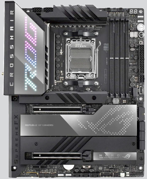
| Processor: | AMD Ryzen 9 9950X 16c/32t |
| Motherboard: | ASUS X670E Crosshair Hero BIOS 2201 |
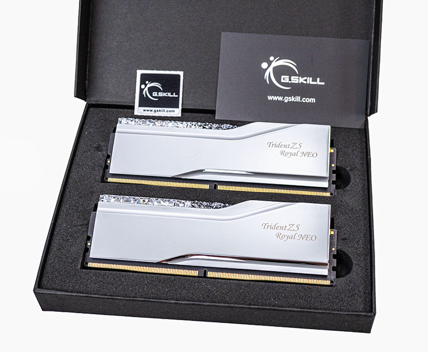
| Memory: | G.Skill Trident Z5 Royal Neo F5-8000J3848H16GX2-TR5NS DDR5-8000 38-48-48-127 / 1.45 V / UCLK 1:2 DDR5-7200 34-42-42-84 / 1.45 V / UCLK 1:2 DDR5-6400 32-38-38-76-156 / 1.45 V / UCLK 1:1 DDR5-6000 28-36-36-72 / 1.45 V / UCLK 1:1 DDR5-4800 40-40-40-77 / 1.1 V (JEDEC) DDR5-5600 40-40-40-77 / 1.1 V (JEDEC) Fabric Clock @ 2100 MHz |
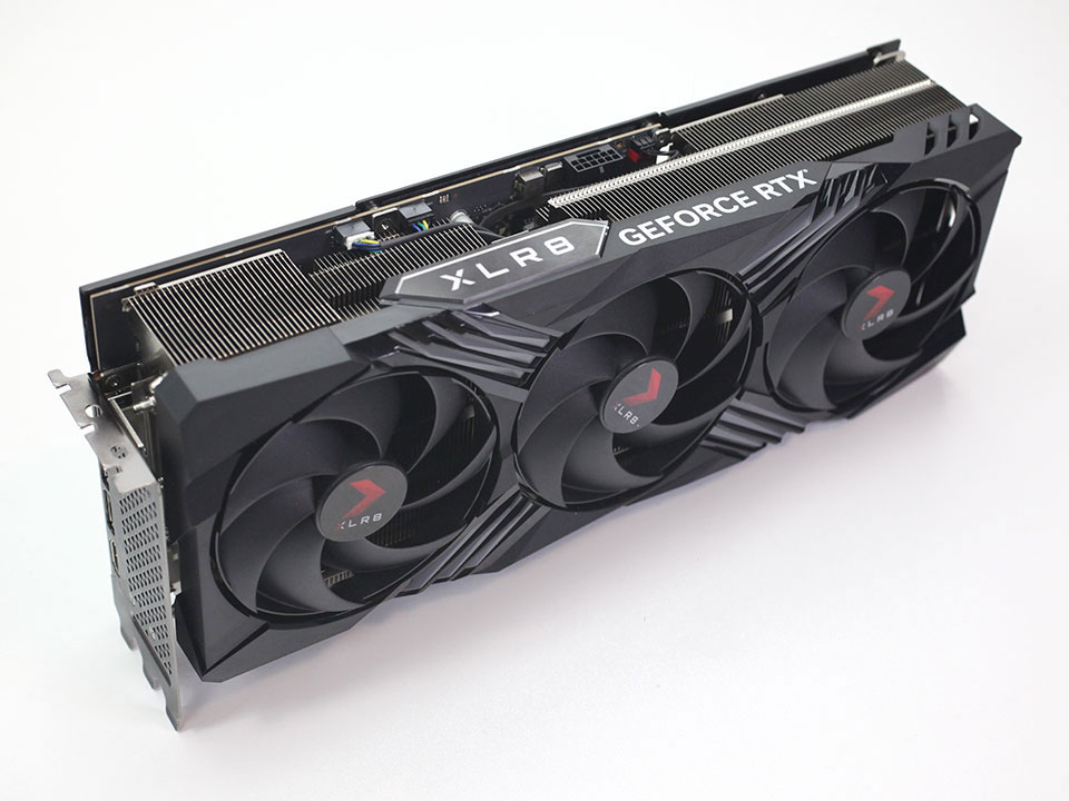
| Graphics: | PNY GeForce RTX 4090 XLR8 |
| Storage: | 2 TB M.2 NVMe SSD |
| Air Cooling: | Noctua NH-D15 |
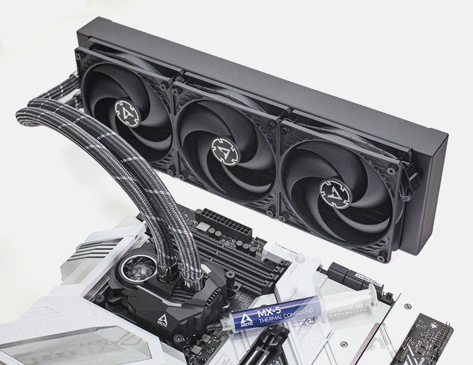
| Water Cooling: | Arctic Liquid Freezer II 420 mm AIO |
| Thermal Paste: | Arctic MX-6 |
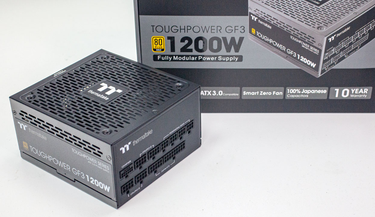
| Power Supply: | Thermaltake Toughpower GF3 1200 W ATX 3.0 / 16-pin 12VHPWR |
| Software: | Windows 11 Professional 64-bit 23H2 VBS enabled (Windows 11 default) |
| Drivers: | NVIDIA GeForce 555.85 WHQL Ryzen Chipset Drivers: 6.06.28.910 Game Mode enabled, Game Bar installed and active |
Jul 2nd, 2025 23:52 CDT
change timezone
Latest GPU Drivers
New Forum Posts
- What Windows is overall the best to you and why? (263)
- Will you buy a RTX 5090? (589)
- NVIDIA App (36)
- AMD RX 7000 series GPU Owners' Club (1327)
- What's your latest tech purchase? (24189)
- RDNA 4 Fine Wine? (HUB Vid) (41)
- GravityMark v1.89 GPU Benchmark (308)
- Good time in the year to buy a new PC (5)
- The Official Thermal Interface Material thread (1767)
- Nvidia drivers (6)
Popular Reviews
- ASUS ROG Crosshair X870E Extreme Review
- Crucial T710 2 TB Review - Record-Breaking Gen 5
- Sapphire Radeon RX 9060 XT Pulse OC 16 GB Review - An Excellent Choice
- PowerColor ALPHYN AM10 Review
- Upcoming Hardware Launches 2025 (Updated May 2025)
- AMD Ryzen 7 9800X3D Review - The Best Gaming Processor
- AVerMedia CamStream 4K Review
- Sapphire Radeon RX 9070 XT Nitro+ Review - Beating NVIDIA
- NVIDIA GeForce RTX 5060 8 GB Review
- AMD Ryzen 9 9950X3D Review - Great for Gaming and Productivity
TPU on YouTube
Controversial News Posts
- Intel's Core Ultra 7 265K and 265KF CPUs Dip Below $250 (288)
- NVIDIA Grabs Market Share, AMD Loses Ground, and Intel Disappears in Latest dGPU Update (212)
- Some Intel Nova Lake CPUs Rumored to Challenge AMD's 3D V-Cache in Desktop Gaming (140)
- NVIDIA GeForce RTX 5080 SUPER Could Feature 24 GB Memory, Increased Power Limits (114)
- NVIDIA Launches GeForce RTX 5050 for Desktops and Laptops, Starts at $249 (105)
- Microsoft Partners with AMD for Next-gen Xbox Hardware (105)
- Intel "Nova Lake‑S" Series: Seven SKUs, Up to 52 Cores and 150 W TDP (100)
- NVIDIA DLSS Transformer Cuts VRAM Usage by 20% (96)