Apr 3rd, 2025 15:55 EDT
change timezone
Latest GPU Drivers
New Forum Posts
- 4x16gb how are these? (9)
- What's your latest tech purchase? (23458)
- Post your CrystalDiskMark speeds (616)
- Help me pick a UPS (46)
- Someone knowledable on memory voltages want to chime in? (also what is PMIC and should I be worried) (1)
- TPU's F@H Team (20416)
- Help me decide if I should buy the arc B580 (As a backup) (10)
- Microprose: Falcon 5.0 - Well under development- yeay (10)
- New posts added to last post (1)
- 5070 cards available below £550 in in the UK (9)
Popular Reviews
- DDR5 CUDIMM Explained & Benched - The New Memory Standard
- Sapphire Radeon RX 9070 XT Pulse Review
- SilverStone Lucid 04 Review
- PowerColor Radeon RX 9070 Hellhound Review
- Sapphire Radeon RX 9070 XT Nitro+ Review - Beating NVIDIA
- Pwnage Trinity CF Review
- Palit GeForce RTX 5070 GamingPro OC Review
- ASRock Phantom Gaming B850 Riptide Wi-Fi Review - Amazing Price/Performance
- AMD Ryzen 7 9800X3D Review - The Best Gaming Processor
- Samsung 9100 Pro 2 TB Review - The Best Gen 5 SSD
Controversial News Posts
- MSI Doesn't Plan Radeon RX 9000 Series GPUs, Skips AMD RDNA 4 Generation Entirely (146)
- Microsoft Introduces Copilot for Gaming (124)
- AMD Radeon RX 9070 XT Reportedly Outperforms RTX 5080 Through Undervolting (119)
- NVIDIA Reportedly Prepares GeForce RTX 5060 and RTX 5060 Ti Unveil Tomorrow (115)
- Over 200,000 Sold Radeon RX 9070 and RX 9070 XT GPUs? AMD Says No Number was Given (100)
- NVIDIA GeForce RTX 5050, RTX 5060, and RTX 5060 Ti Specifications Leak (96)
- Retailers Anticipate Increased Radeon RX 9070 Series Prices, After Initial Shipments of "MSRP" Models (90)
- China Develops Domestic EUV Tool, ASML Monopoly in Trouble (88)
 19
19
EVGA GeForce RTX 3080 Ti FTW3 Ultra Review
Test Setup »High-resolution PCB Pictures
These pictures are for the convenience of volt modders and people who would like to see all the finer details on the PCB. Feel free to link back to us and use these in your articles, videos or forum posts.

High-res versions are also available (front, back).
Circuit Board (PCB) Analysis

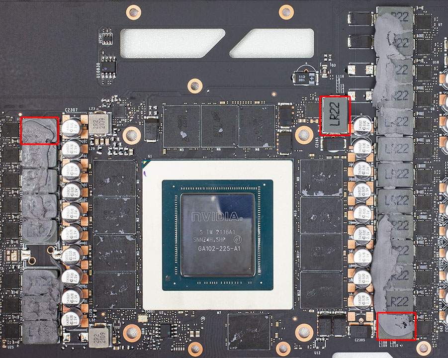
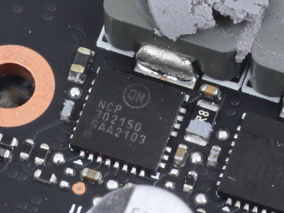
The GPU VRM is 19-phase, controlled by two OnSemi NCP8610 controllers.

OnSemi NCP302150 DrMOS chips pull the GPU power phases.

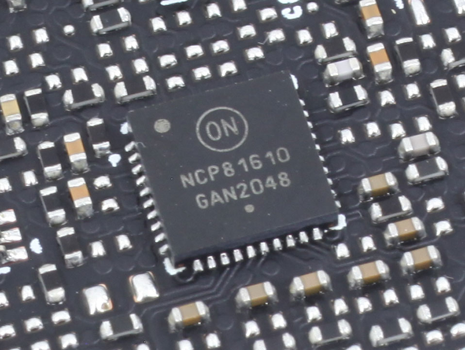
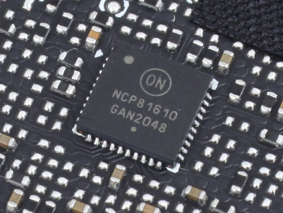
Memory is a 3-phase setup pulled by an OnSemi NCP81610 controller.
OnSemi NCP302150 DrMOS make another appearance, this time working the memory phases.
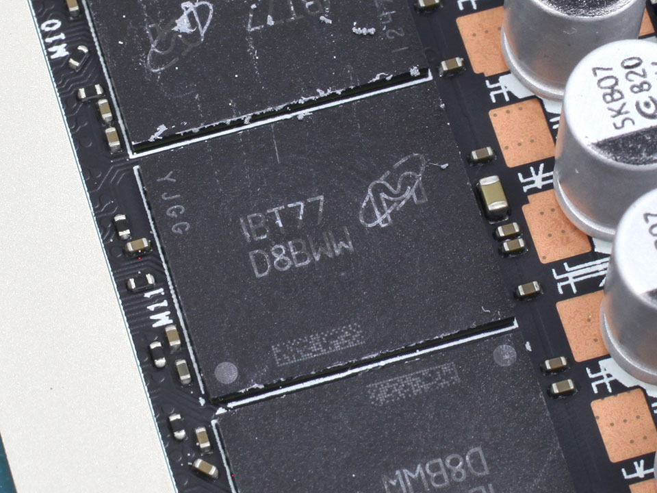
The GDDR6X memory chips are made by Micron and carry the model number D8BWW, which decodes to MT61K256M32JE-19G:T. They are specified to run at 1188 MHz (19 Gbps GDDR6X effective).
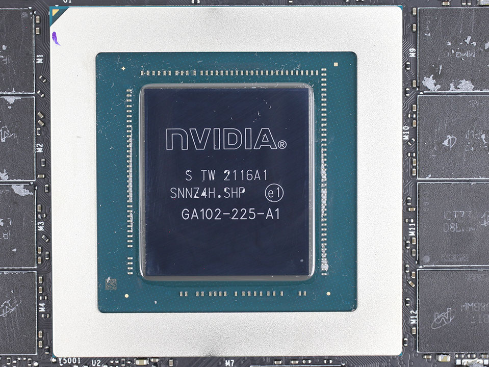
NVIDIA's GA102 graphics processor is the company's second Ampere architecture chip, the first one targeted at GeForce gamers. It is produced on a 8 nanometer process at Samsung and has a transistor count of 28 billion with a die size of 628 mm².
Apr 3rd, 2025 15:55 EDT
change timezone
Latest GPU Drivers
New Forum Posts
- 4x16gb how are these? (9)
- What's your latest tech purchase? (23458)
- Post your CrystalDiskMark speeds (616)
- Help me pick a UPS (46)
- Someone knowledable on memory voltages want to chime in? (also what is PMIC and should I be worried) (1)
- TPU's F@H Team (20416)
- Help me decide if I should buy the arc B580 (As a backup) (10)
- Microprose: Falcon 5.0 - Well under development- yeay (10)
- New posts added to last post (1)
- 5070 cards available below £550 in in the UK (9)
Popular Reviews
- DDR5 CUDIMM Explained & Benched - The New Memory Standard
- Sapphire Radeon RX 9070 XT Pulse Review
- SilverStone Lucid 04 Review
- PowerColor Radeon RX 9070 Hellhound Review
- Sapphire Radeon RX 9070 XT Nitro+ Review - Beating NVIDIA
- Pwnage Trinity CF Review
- Palit GeForce RTX 5070 GamingPro OC Review
- ASRock Phantom Gaming B850 Riptide Wi-Fi Review - Amazing Price/Performance
- AMD Ryzen 7 9800X3D Review - The Best Gaming Processor
- Samsung 9100 Pro 2 TB Review - The Best Gen 5 SSD
Controversial News Posts
- MSI Doesn't Plan Radeon RX 9000 Series GPUs, Skips AMD RDNA 4 Generation Entirely (146)
- Microsoft Introduces Copilot for Gaming (124)
- AMD Radeon RX 9070 XT Reportedly Outperforms RTX 5080 Through Undervolting (119)
- NVIDIA Reportedly Prepares GeForce RTX 5060 and RTX 5060 Ti Unveil Tomorrow (115)
- Over 200,000 Sold Radeon RX 9070 and RX 9070 XT GPUs? AMD Says No Number was Given (100)
- NVIDIA GeForce RTX 5050, RTX 5060, and RTX 5060 Ti Specifications Leak (96)
- Retailers Anticipate Increased Radeon RX 9070 Series Prices, After Initial Shipments of "MSRP" Models (90)
- China Develops Domestic EUV Tool, ASML Monopoly in Trouble (88)