 22
22
Inno3D GeForce GTX 295 Platinum (Single PCB) Review
Test Setup »A Closer Look
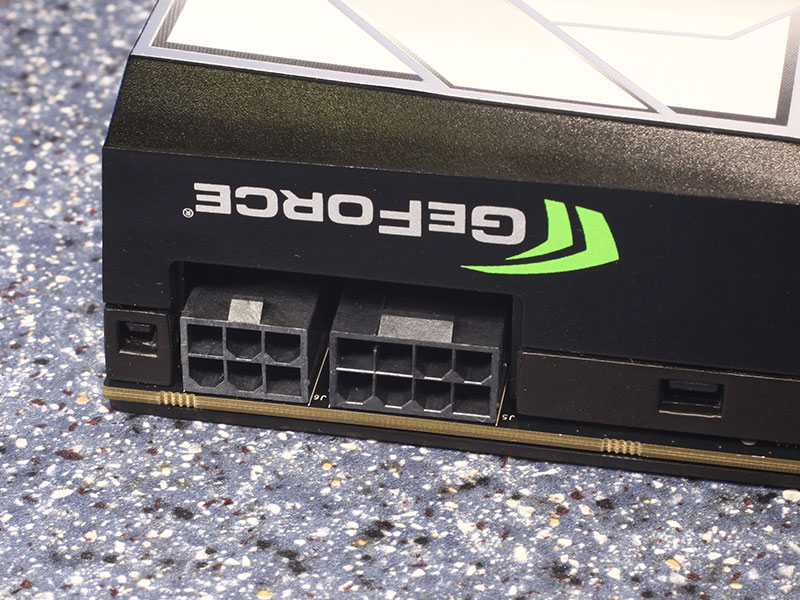
Power is delivered to the card via a six pin and one eight pin power connector. Both are required to run, it won't work with just one connected.
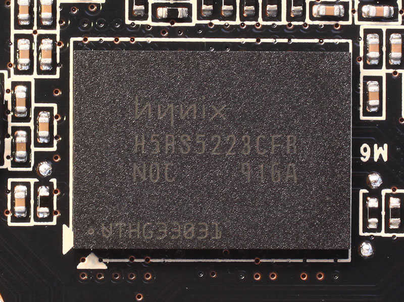
The GDDR3 memory chips are made by Hynix and carry the model number H5RS5223CFR-N0C. With a cycle time of 1.0 ns, they are specified to run at 1000 MHz.
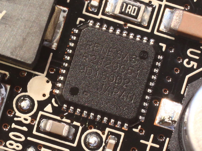
Eight of these Renesas R2J20651NP DrMos MOSFET chips are located on the board, four for each GPU. Each one incorporates a high-side FET, low-side FET and driver in a single package - essentially one PWM phase. Such a high-density design helps to reduce the PCB area consumption and also reduces the complexity of sourcing parts.
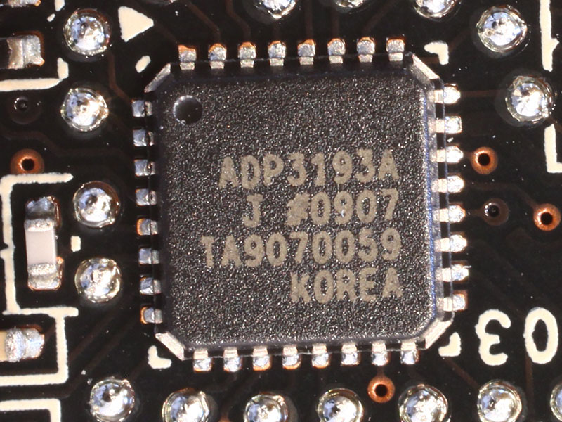
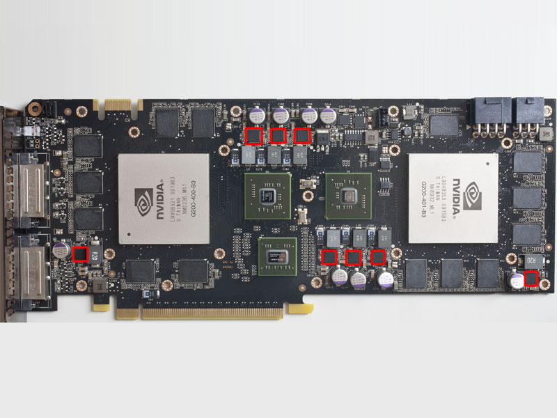
Instead of the well-known Volterra voltage controllers that allow software voltage control, NVIDIA has chosen to go with the ADP3193A voltage controller this time. Unfortunately it doesn't support I2C which means software voltage control is not possible. The datasheet is available online, so voltmodders can easily have a go at hardmodding their cards.
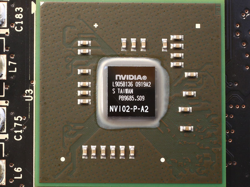
NVIDIA has separated the display output logic from the GPU on the latest chips. So in order to drive the two DVI outputs a single NVIO chip is required. Why there is a second chip, I don't know, it shouldn't be needed to drive two outputs.
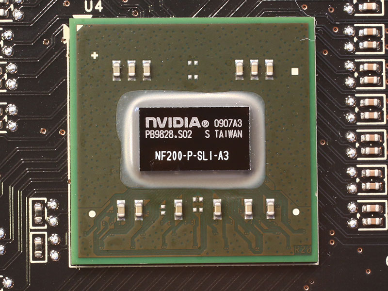
NVIDIA is using their own NF200 PCI-Express bridge chip to interconnect both GPUs. AMD uses a chip from another manufacturer for their HD 4870 X2. NVIDIA's chip offers some additional features which are supposed to help with SLI performance, we have also seen several motherboard designs on which the NF200 is used.
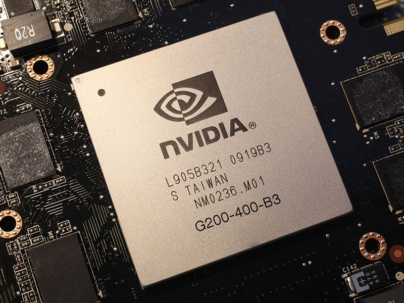
Here you can see the two GT200b GPUs that power the GTX 295. Each which is made in a 55 nm process at TSMC Taiwan with 1.4 billion transistors.
Dec 24th, 2024 07:27 EST
change timezone
Latest GPU Drivers
New Forum Posts
- 3D Printer Club (355)
- Post Your TIMESPY, PCMARK10 & FIRESTRIKE SCORES! (2019) (264)
- enclosure cases interfere commands sent windows for hdd? (1)
- ChatGPT (3)
- Show Us Your Computer Workbench (12)
- [SOLVED] Frametime spikes/Stutters/FPS drops in all games. (281)
- NVIDIA GeForce RTX 5000 Series “Blackwell” TDPs Leaked, Entire Lineup Unified with 12+4 Pin Power Connector (86)
- Trying to understand EDP OTHER and BD PROCHOT warnings (8)
- Solidigm NVMe Custom Modded Driver for All NVMe Brands SSDs & Any NVMe SSDs (179)
- AAF Optimus Modded Driver For Windows 10 & Windows 11 - Only for Realtek HDAUDIO Chips (219)
Popular Reviews
- Arrow Lake Retested with Latest 24H2 Updates and 0x114 Microcode
- Team Group T-FORCE Dark AirFlow I SSD Cooler Review
- EIZO FlexScan EV3240X Review - It Means Business
- Intel Arc B580 Review - Excellent Value
- HyperX Alloy Origins Keyboard Review
- AMD Ryzen 7 9800X3D Review - The Best Gaming Processor
- Montech MKey PRO Wireless Mechanical Keyboard Review
- ASRock Arc B580 Steel Legend Review
- DUNU DK3001BD In-Ear Monitors Review - Brain Dance Time!
- Upcoming Hardware Launches 2024 (Updated Nov 2024)
Controversial News Posts
- Intel CEO Pat Gelsinger Retires, Company Appoints two Interim co-CEOs (217)
- AMD Radeon RX 8800 XT RDNA 4 Enters Mass-production This Month: Rumor (215)
- 32 GB NVIDIA RTX 5090 To Lead the Charge As 5060 Ti Gets 16 GB Upgrade and 5060 Still Stuck With Last-Gen VRAM Spec (167)
- NVIDIA GeForce RTX 5070 Ti Leak Tips More VRAM, Cores, and Power Draw (160)
- AMD Radeon RX 8800 XT Reportedly Features 220 W TDP, RDNA 4 Efficiency (123)
- AMD Radeon "RX 8800 XT" is Actually the RX 9070 XT? (105)
- NVIDIA Blackwell RTX and AI Features Leaked by Inno3D (90)
- Intel 18A Process Node Clocks an Abysmal 10% Yield: Report (90)