 60
60
Intel Core i5-10600K Review - All You Need for Gaming
Test Setup »Architecture


Under the hood of the Core i5-10600K is the 6-core "Comet Lake-S" silicon built on the same 14 nm++ process as the previous two generations, but with one key difference: Intel physically thinned the die along the Z-axis by removing as much of the silicon bulk as possible, the idea being that heat generated by the die travels through less silicon. The more conductive copper integrated heatspreader has been made thicker, and a solder thermal interface material (STIM) is used between the two. The die area is estimated to be 149.6 mm². This die looks similar to the 6-core "Coffee Lake" or "Coffee Lake Refresh" dies, but has the die thinning innovation.

The "Comet Lake-S" silicon is laid out similar to the past four generations of Intel mainstream processors, with two rows of CPU cores flanked by the iGPU on one side and the system agent (integrated northbridge) on the other, and a Ringbus Interconnect serving as town square between the various components. The last-level cache is scattered across as slices of 1 MB or 2 MB, adding up to 12 MB of unified L3 cache all cores can access equally.
Much of the processor's uncore components are clumped into the System Agent, which contains the memory controller, PCI-Express gen 3.0 root-complex, DMI interface, and memory PHY. On the other end of the ringbus is the Gen 9.5 integrated graphics, which has practically been carried over for the past three generations, featuring 24 execution units in the GT2 trim. All SKUs in the desktop 10th gen processor series appear to have the top GT2 trim. Don't expect to play PUBG at 4K on this; the "UHD" moniker only indicates that the IGP can handle 4K Ultra HD displays, features modern connectivity options, such as DP 1.4 and HDMI 2.0, and can playback 4K video in new formats with 10-bpc color and HDR10/Dolby Vision standards.

The core itself is identical in design to "Skylake," and there are hence no IPC increases to be had. As we explained in the introduction, all of Intel's efforts to increase gaming, single-threaded, and less-parallelized application performance revolves around increasing the clock speeds, and deploying as many as three intelligent boosting algorithms to achieve the advertised clock speeds.
The Core i5-10600K has a nameplate base frequency (aka nominal clock) of 4.10 GHz, and a maximum Turbo Boost frequency of 4.80 GHz. Unlike the Core i9-10900K, it lacks Turbo Boost Max 3.0 or Thermal Velocity Boost. It still has significantly increased power limits compared to something like a Core i7-8700K, with PL1 set at 125 W and PL2 at 182 W, with a 56-second Tau (time value at which the processor is allowed to sustain elevated power levels before having to drop down to nominal clocks).
Motherboard manufacturers have been given the freedom to override PL2 and Tau as they see fit, and so various motherboards implement power limits differently depending on the effectiveness of their VRM solution. You are hence rewarded for buying a pricier motherboard that has a better VRM, and a more aggressive vendor-supplied power-management. Of course, all boards come with Intel-spec fallbacks.
Intel introduced a handful of overclocking enhancements with the 10th generation, including the ability to toggle HyperThreading on a per-core basis rather than globally. This could be an interesting option for those gaming and streaming, where a certain number of cores have HTT disabled for the best gaming performance and certain cores have them enabled, with Windows process core-affinity settings taking care of the rest.
The company also introduced the ability to overclock the DMI chipset bus. DMI is a PCIe-based interconnect that handles transfers between the processor and the chipset (PCH). The LGA1200 platform uses DMI 3.0 (comparable to PCI-Express 3.0 x4 in terms of bandwidth). Intel has apparently decoupled PCIe clock domains to enable you to overclock the DMI and PEG (that topmost x16 PCIe slot) without destabilizing your PCIe setup for graphics cards. The refreshed Extreme Tuning Utility now comes with finer-grained control of the voltage-frequency curve. The company also updated the Performance Maximizer app that automates overclocking using the trial-and-error method.
The Z490 Platform
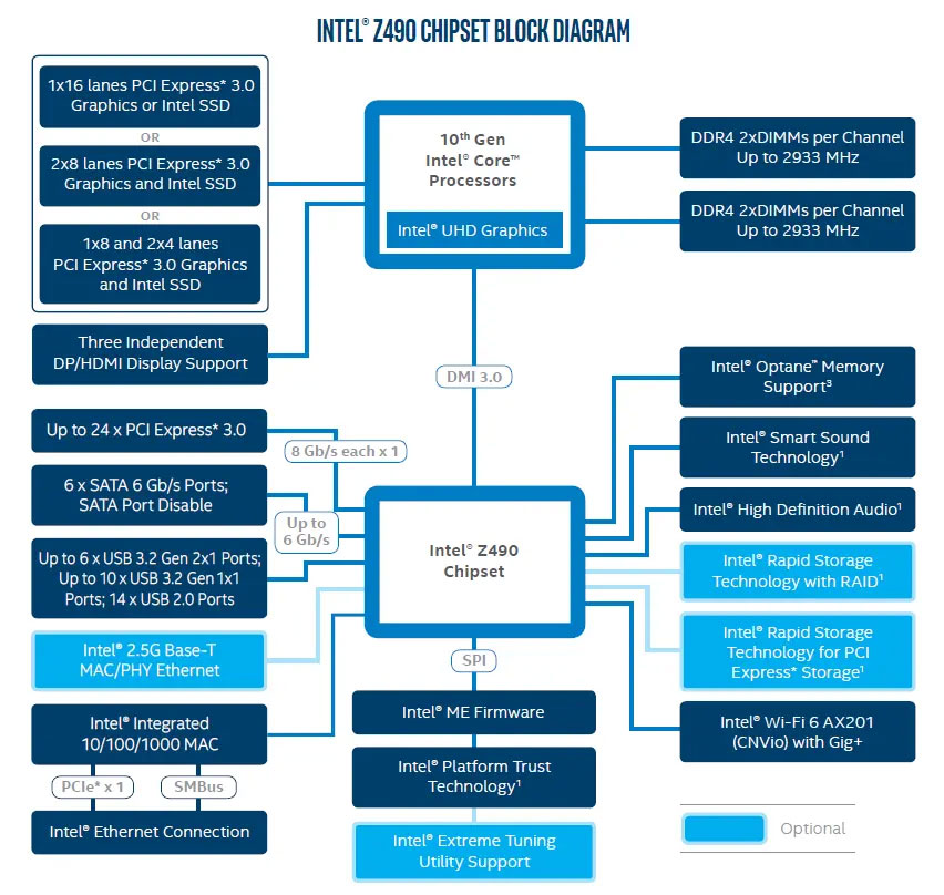
Z490 is the top 400-series chipset targeted at gaming desktops and PC enthusiasts, as it enables serious overclocking and multi-GPU support. In terms of I/O capabilities, the chipset is nearly identical to the Z390, with 24 downstream PCIe gen 3.0 lanes, six SATA ports, six USB 3.2 gen 2 ports that can be converted to three USB 3.2 gen 2x2 ports, ten USB 3.2 gen 1 ports, and fourteen USB 2.0 ports. Intel is recommending its i225-V 2.5 Gbps Ethernet chip as the wired networking solution to go with Z490, and the company's AX201 802.11ax WiFi 6 WLAN solution to go with the chipset's CNVio interface.
Jul 12th, 2025 05:18 CDT
change timezone
Latest GPU Drivers
New Forum Posts
- Gigabyte graphic cards - TIM gel SLIPPAGE problem (146)
- What's your latest tech purchase? (24240)
- Best motherboards for XP gaming (103)
- ASUS ProArt GeForce RTX 4060 Ti OC Edition 16GB GDDR6 Gaming - nvflash64 VBIOS mismatch (3)
- Steam Deck Owners Clubhouse (535)
- What are you playing? (23923)
- Chrome has removed uBlock Origin 1.64.0 (remove google search suggestions) (0)
- Can you guess Which game it is? (227)
- Will you buy a RTX 5090? (645)
- 'NVIDIA App' not usable offline? (9)
Popular Reviews
- Fractal Design Epoch RGB TG Review
- Corsair FRAME 5000D RS Review
- Lexar NM1090 Pro 4 TB Review
- NVIDIA GeForce RTX 5050 8 GB Review
- NZXT N9 X870E Review
- Sapphire Radeon RX 9060 XT Pulse OC 16 GB Review - An Excellent Choice
- Our Visit to the Hunter Super Computer
- AMD Ryzen 7 9800X3D Review - The Best Gaming Processor
- Upcoming Hardware Launches 2025 (Updated May 2025)
- Chieftec Iceberg 360 Review
TPU on YouTube
Controversial News Posts
- Intel's Core Ultra 7 265K and 265KF CPUs Dip Below $250 (288)
- Some Intel Nova Lake CPUs Rumored to Challenge AMD's 3D V-Cache in Desktop Gaming (140)
- AMD Radeon RX 9070 XT Gains 9% Performance at 1440p with Latest Driver, Beats RTX 5070 Ti (131)
- NVIDIA Launches GeForce RTX 5050 for Desktops and Laptops, Starts at $249 (119)
- NVIDIA GeForce RTX 5080 SUPER Could Feature 24 GB Memory, Increased Power Limits (115)
- Microsoft Partners with AMD for Next-gen Xbox Hardware (105)
- Intel "Nova Lake‑S" Series: Seven SKUs, Up to 52 Cores and 150 W TDP (100)
- NVIDIA DLSS Transformer Cuts VRAM Usage by 20% (97)