 332
332
Intel Core i5-12600K Review - Winning Price/Performance
(332 Comments) »Introduction
The Core i5-12600K "Alder Lake" is Intel's all-important performance-segment processor around the $290-mark, taking the fight to the AMD Ryzen 5 5600X and perhaps even Ryzen 7 5800X. Before Ryzen shook things up in the processor industry, Core i5 in the desktop segment consisted of 4-core/4-thread processors for the longest time, but has since seen its core-counts go up every two years in response to AMD's consistent generational performance gains. The 8th and 9th Gen Core i5 chips were 6-core/6-thread, while the 10th and 11th Gen ones were 6-core/12-thread, matching their Ryzen 5 counterparts. "Alder Lake" introduces the Hybrid core architecture to the desktop segment, where we see combinations of larger performance "P" cores alongside efficient "E" cores, with the Intel Thread Director middleware working at a low level with the operating system to ensure the right kind of workload for the two core types.

The Core i5-12600K we're reviewing today is technically a 10-core/16-thread processor featuring six performance cores that have HyperThreading enabled, and four efficiency cores that lack it—hence the asymmetric thread count. Intel claims that its "Golden Cove" performance cores offer a massive 28% IPC gain over the "Skylake" cores that powered five generations of Core processors; and an impressive 19% gain over the "Cypress Cove" cores powering the previous-gen "Rocket Lake." On paper, the "Gracemont" E-cores are quite something else, matching the "Skylake" cores in IPC at the right frequency for a fraction of the power. These also only take up a quarter of the die area of the larger P-cores.
The two core types operate at different clock-speed bands. The P-cores tick at 3.70 GHz base and 4.90 GHz boost, while the E-cores do 2.80 GHz base with 3.60 GHz boost. Each of the six P-cores has 1.25 MB of dedicated L2 cache, while the four E-cores share 2 MB of L2 cache. All ten cores share 20 MB of L3 cache. Intel has done away with the vague terminology of TDP with this generation and defined two power values relevant to the consumer. For the i5-12600K, 125 W is set as the processor Base Power Value, while the Maximum Turbo Power value is set at 150 W. The processor can be made to operate at Maximum Turbo Power indefinitely or swing between the two values across various power levels.
The 12th Gen Core "Alder Lake" processors introduce new-generation I/O, including PCI-Express Gen 5, although only for the x16 PEG slot. The CPU-attached M.2 NVMe slot is still Gen 4. The processors are also first to market with DDR5 memory support, but retain backwards compatibility with DDR4. Intel ensured that motherboard manufacturers have plenty of products with DDR4 slots, should you want to stick to your current memory. The chipset bus sees a doubling in bandwidth over the previous generation, and there is chipset-attached PCIe Gen 4 connectivity.
| Price | Cores / Threads | Base Clock | Max. Boost | L3 Cache | TDP | Architecture | Process | Socket | |
|---|---|---|---|---|---|---|---|---|---|
| Core i5-9400F | $170 | 6 / 6 | 2.9 GHz | 4.1 GHz | 9 MB | 65 W | Coffee Lake | 14 nm | LGA 1151 |
| Core i5-10400F | $180 | 6 / 12 | 2.9 GHz | 4.3 GHz | 12 MB | 65 W | Comet Lake | 14 nm | LGA 1200 |
| Core i5-11400F | $215 | 6 / 12 | 2.6 GHz | 4.4 GHz | 12 MB | 65 W | Rocket Lake | 14 nm | LGA 1200 |
| Core i5-10500 | $225 | 6 / 12 | 3.1 GHz | 4.5 GHz | 12 MB | 65 W | Comet Lake | 14 nm | LGA 1200 |
| Ryzen 5 3600 | $230 | 6 / 12 | 3.6 GHz | 4.2 GHz | 32 MB | 65 W | Zen 2 | 7 nm | AM4 |
| Core i5-9600K | $210 | 6 / 6 | 3.7 GHz | 4.6 GHz | 9 MB | 95 W | Coffee Lake | 14 nm | LGA 1151 |
| Core i5-10600K | $260 | 6 / 12 | 4.1 GHz | 4.8 GHz | 12 MB | 125 W | Comet Lake | 14 nm | LGA 1200 |
| Core i5-11600K | $260 | 6 / 12 | 3.9 GHz | 4.9 GHz | 12 MB | 125 W | Rocket Lake | 14 nm | LGA 1200 |
| Ryzen 5 3600X | $290 | 6 / 12 | 3.8 GHz | 4.4 GHz | 32 MB | 95 W | Zen 2 | 7 nm | AM4 |
| Ryzen 5 5600G | $250 | 6 / 12 | 3.9 GHz | 4.4 GHz | 16 MB | 65 W | Zen 3 + Vega | 7 nm | AM4 |
| Ryzen 5 5600X | $310 | 6 / 12 | 3.7 GHz | 4.6 GHz | 32 MB | 65 W | Zen 3 | 7 nm | AM4 |
| Core i5-12600K | $300 | 6+4 / 16 | 3.7 / 2.8 GHz | 4.9 / 3.6 GHz | 20 MB | 125 W | Alder Lake | 10 nm | LGA 1700 |
| Core i7-9700K | $310 | 8 / 8 | 3.6 GHz | 4.9 GHz | 12 MB | 95 W | Coffee Lake | 14 nm | LGA 1151 |
| Core i7-10700K | $330 | 8 / 16 | 3.8 GHz | 5.1 GHz | 16 MB | 125 W | Comet Lake | 14 nm | LGA 1200 |
| Core i7-11700K | $350 | 8 / 16 | 3.6 GHz | 5.0 GHz | 16 MB | 125 W | Rocket Lake | 14 nm | LGA 1200 |
| Ryzen 7 3700X | $320 | 8 / 16 | 3.6 GHz | 4.4 GHz | 32 MB | 65 W | Zen 2 | 7 nm | AM4 |
| Ryzen 7 5700G | $350 | 8 / 16 | 3.8 GHz | 4.6 GHz | 16 MB | 65 W | Zen 3 + Vega | 7 nm | AM4 |
| Ryzen 7 3800XT | $400 | 8 / 16 | 3.9 GHz | 4.7 GHz | 32 MB | 105 W | Zen 2 | 7 nm | AM4 |
| Core i7-12700K | $420 | 8+4 / 20 | 3.6 / 2.7 GHz | 5.0 / 3.8 GHz | 25 MB | 125 W | Alder Lake | 10 nm | LGA 1700 |
| Ryzen 7 5800X | $400 | 8 / 16 | 3.8 GHz | 4.7 GHz | 32 MB | 105 W | Zen 3 | 7 nm | AM4 |
| Core i9-10900 | $440 | 10 / 20 | 2.8 GHz | 5.2 GHz | 20 MB | 65 W | Comet Lake | 14 nm | LGA 1200 |
| Ryzen 9 3900X | $430 | 12 / 24 | 3.8 GHz | 4.6 GHz | 64 MB | 105 W | Zen 2 | 7 nm | AM4 |
| Ryzen 9 5900X | $525 | 12 / 24 | 3.7 GHz | 4.8 GHz | 64 MB | 105 W | Zen 3 | 7 nm | AM4 |
| Core i9-9900K | $470 | 8 / 16 | 3.6 GHz | 5.0 GHz | 16 MB | 95 W | Coffee Lake | 14 nm | LGA 1151 |
| Core i9-10900K | $470 | 10 / 20 | 3.7 GHz | 5.3 GHz | 20 MB | 125 W | Comet Lake | 14 nm | LGA 1200 |
| Core i9-11900K | $550 | 8 / 16 | 3.5 GHz | 5.3 GHz | 16 MB | 125 W | Rocket Lake | 14 nm | LGA 1200 |
| Ryzen 9 3950X | $765 | 16 / 32 | 3.5 GHz | 4.7 GHz | 64 MB | 105 W | Zen 2 | 7 nm | AM4 |
| Ryzen 9 5950X | $750 | 16 / 32 | 3.4 GHz | 4.9 GHz | 64 MB | 105 W | Zen 3 | 7 nm | AM4 |
| Core i9-12900K | $600 | 8+8 / 24 | 3.2 / 2.4 GHz | 5.2 / 3.9 GHz | 30 MB | 125 W | Alder Lake | 10 nm | LGA 1700 |

Intel paper-launched the 12th Gen Core processor family on October 27, allowing us to post everything about the processor except performance testing, so we did a more comprehensive Preview Article on the "Alder Lake" microarchitecture. "Alder Lake-S" is the first desktop processor silicon built by Intel on its Intel 7 silicon fabrication node, formerly known as 10 nm Enhanced SuperFin. This node offers comparable transistor-density and power characteristics as 7 nm-class nodes by TSMC. The die measures approximately 200 mm², although it is noticeably smaller than the 14 nm "Rocket Lake-S" die.


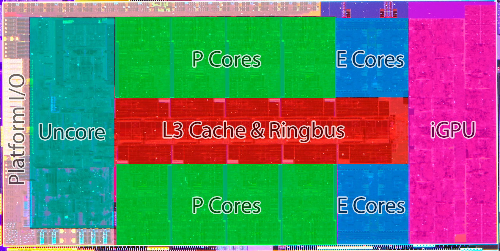
The monolithic silicon features 8 "Golden Cove" P and 8 "Gracemont" E-cores. The E-cores are spread across two 4-core "E-core Clusters." A bi-directional Ringbus and 30 MB of L3 cache connect the P-cores, and E-core clusters, with the Uncore (integrated northbridge) and iGPU. The chip features a dual-mode memory controller that supports 160-bit wide DDR5 (native support for DDR5-4800) or 128-bit wide DDR4 (native support for DDR4-3200). The Gen12 Xe LP iGPU is carried over almost unchanged from the "Rocket Lake-S" silicon, with a minor speed-bump. The PCI-Express root complex is fascinating. The silicon puts out 16 Gen 5 lanes (32 Gbps per lane), which are allocated to the PEG slot on the motherboard, and 12 Gen 4 lanes (16 Gbps per lane), of which four drive a CPU-attached M.2 NVMe slot and eight serve as a physical layer of the DMI 4.0 x8 chipset bus (128 Gbps per direction bandwidth).
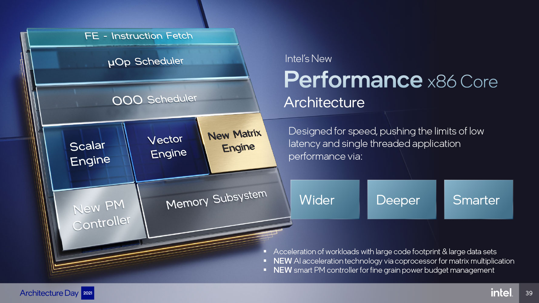

The "Golden Cove" performance core (P-core) features numerical increments to the decode unit, micro-op queue, and micro-op cache. The out-of-order (OoO) engine sees similar increments with 6-wide allocation and 12-wide execution ports, compared to 5-wide allocation and 10-wide execution ports for Cypress Cove. The execution stage sees the addition of a fifth execution port and ALU, FMA with FP16 support, and an updated fast adder (FADD). Similar improvements are made to the cache and memory sub-system. These add toward the 28% IPC uplift for this core. The E-core, on the other hand, is designed to provide a massive performance uplift from the previous-generation "Tremont" low-power microarchitecture, mainly to give it certain ISA capabilities found in larger cores, such as AVX2. The front-end is upgraded with a double-size 64 KB L1 instruction cache, more powerful branch-prediction unit, and two sets of triple out-of-order decoders. The out-of-order engine features a wide 256-entry OoO window and 17 execution ports for more parallelism. The execution stage sees a near 33% increase in both scalar and vector execution stages, as well as double the load store.

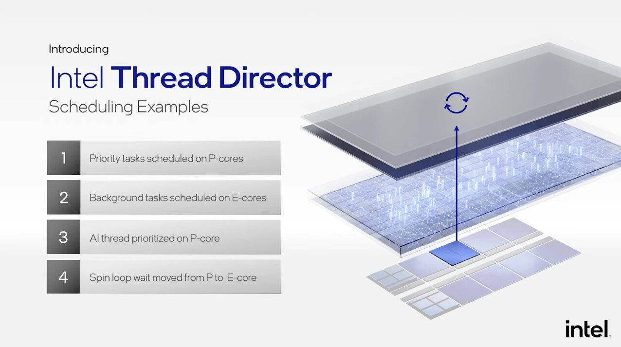
Intel Thread Director is a vital component that ensures the operating system doesn't see "Alder Lake" as having the same kind of CPU cores, sending processing traffic uniformly to all cores. Instead, it gives the OS a degree of awareness of the Hybrid architecture and ensures certain kinds of tasks are allocated exclusively on P-cores and others on E-cores. It also senses the nature of the processing workload (whether it's running in the foreground or background) and decides which kind of cores to tie it to. The OS scheduler by itself moves traffic between cores to meet certain power/thermal objectives, but Thread Director ensures this movement doesn't break the core-type hierarchy. Windows 11 is the recommended version of Windows for Alder Lake, as it introduces the ability for software to inform the processor of the nature of its work, and the kind of cores it's comfortable getting processed by.

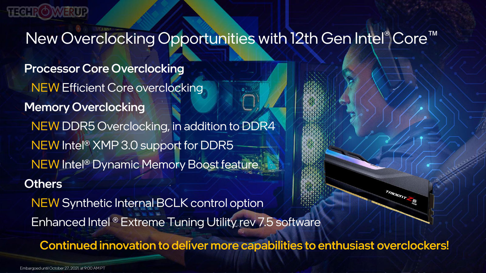
Intel pulled off some innovative ways to transfer heat between the silicon and cooling solution over the past couple of solutions, to eke out the best-possible thermals from the 14 nm node it was stuck with. These innovations continue with Alder Lake. The die and STIM are now thinner and the copper IHS thicker. Among the new overclocking capabilities are the ability to tweak even the E-cores, DDR5 memory, new XMP 3.0 profiles for DDR5 memory, synthetic BCLK that ensures a base-clock overclock doesn't break sensitive clock domains relying on it, and external clock generation, in addition to the processor's internal clock generator.
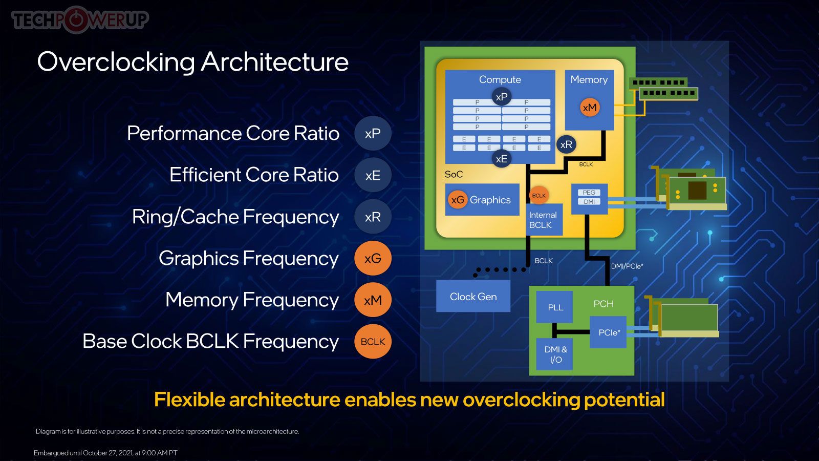
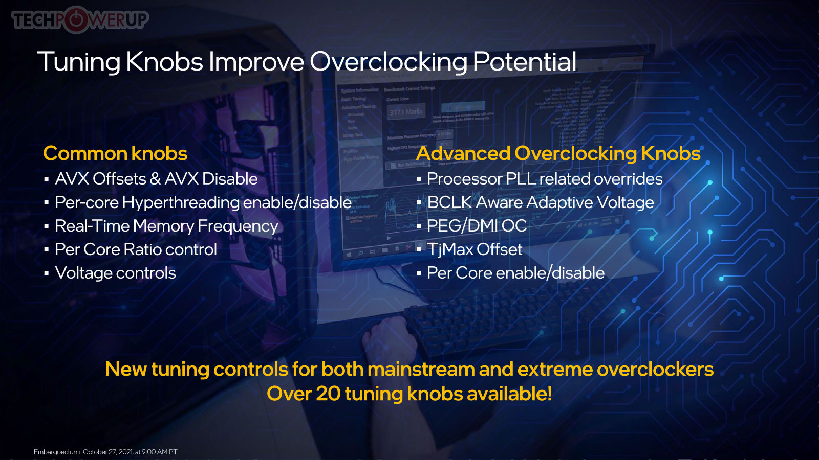
With the monolithic silicon gaining complexity, there are several new overclocking knobs and clock domains to maximize your overclock. The introduction of the E-core adds its own base-clock multiplier, called xE, which works separately from the core ratio of the P-cores, dubbed xP. The xG multiplier dictates iGPU frequency. xR dictates the frequency at which the Ringbus interconnect and L3 cache operate.
Intel Z690 Chipset
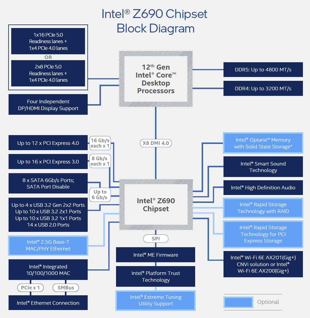
Intel is debuting its 12th Gen Core desktop processors in 2021 exclusively with only the unlocked "K" and "KF" variants, so it's only launching the companion Z690 chipset. The "locked" processor SKUs and value-ended chipsets are expected to join the product stack in 2022. The Z690 chipset is Intel's first client chipset with PCI-Express 4.0 downstream connectivity. It talks to the "Alder Lake-S" processor over the DMI 4.0 x8 chipset bus. Downstream PCIe connectivity includes 12x Gen 4 and 16x Gen 3 PCIe general-purpose lanes. The rest of its chipset-attached connectivity is the same as for Z590, including MIPI SoundWire support, NVMe RAID, 8-port SATA 6 Gbps, and the recommended network interfaces that include 2.5 GbE and Wi-Fi 6E.
Unboxing and Photography
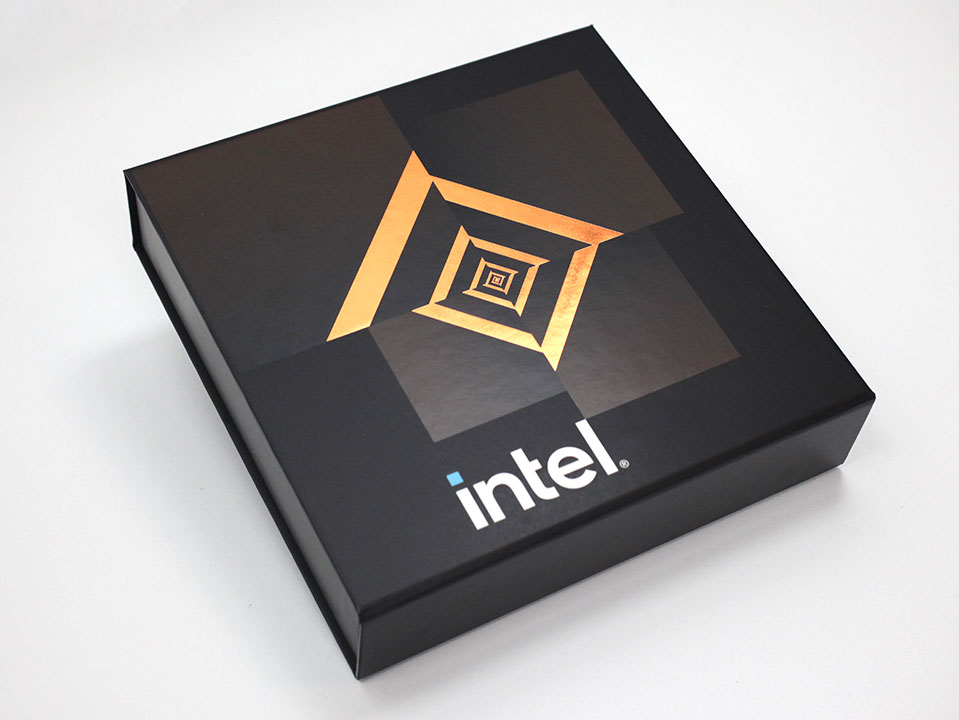


Our Core i9-12900K and i5-12600K samples came to us in a special press-only package, which is a jewel case that has a plastic scale-up model of the Intel Alder Lake-S die.

The retail package is a simple paperboard box that's extremely spartan and doesn't even cost a dollar to make. No cooler is included.


Here it is, the processor itself. It measures 37.5 mm x 45.0 mm and is a more rectangular-looking processor, much like the LGA1366 before it.

Intel Socket LGA1700 has an intuitive installation process that should be familiar from many past LGA sockets. Trouble is that it has a different cooler mount-hole spacing than LGA1200 and five different Socket-H series sockets before it, so you'll need to search for a compatible cooler. Most cooler companies are handing out adapters, but these aren't available in all countries.
Test Setup
- All applications, games, and processors are tested with the drivers and hardware listed below—no performance results were recycled between test systems.
- All games and applications are tested using the same version.
- All games are set to their highest quality setting unless indicated otherwise.
| Test System "Alder Lake" | |
|---|---|
| Processor: | All Intel 12th Generation processors |
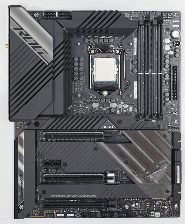
| Motherboard: | ASUS Z690 Maximus Hero BIOS 0702 |
| Memory: | 2x 16 GB G.SKILL Trident Z5 RGB DDR5-6000 36-36-36-76 2T Gear 2 |
| Graphics: | EVGA GeForce RTX 3080 FTW3 Ultra |
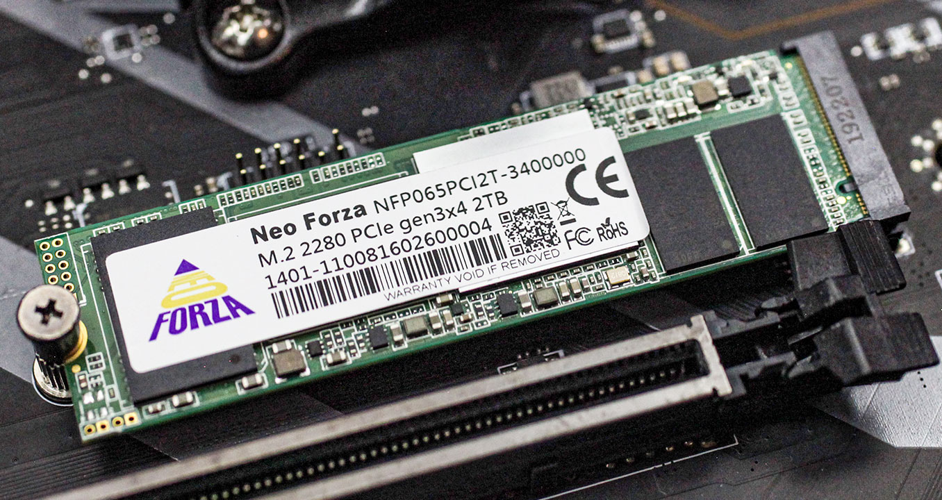
| Storage: | Neo Forza NFP065 1 TB M.2 NVMe SSD |
| Air Cooling: | Noctua NH-U14S |
| Water Cooling: | Arctic Liquid Freezer II 360 mm |
| Thermal Paste: | Arctic MX-5 |
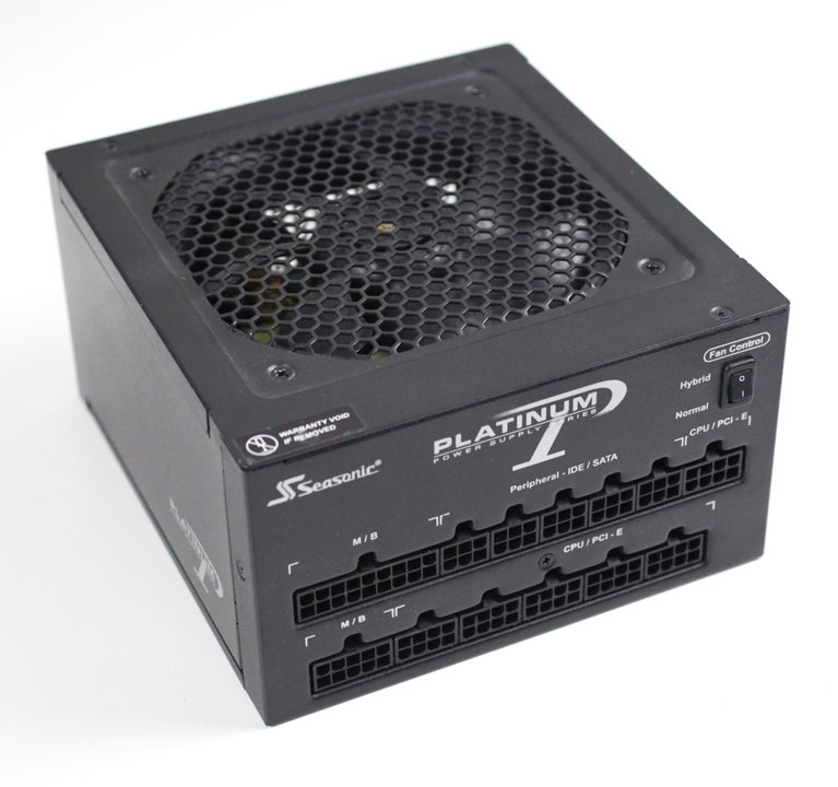
| Power Supply: | Seasonic SS-860XP |
| Software: | Windows 11 Professional 64-bit Build 10.0.22000.282 Includes AMD L3 latency fix |
| Drivers: | NVIDIA GeForce 496.49 WHQL |


| Test System "Zen 3" | |
|---|---|
| Processor: | All AMD Ryzen 5000 |
| Motherboard: | MSI MPG X570 Gaming Plus BIOS 7C37vAF3, AGESA 1.2.0.3c |
| Memory: | 2x 16 GB DDR4-3600 16-20-20-34 1T Infinity Fabric @ 1800 MHz 1:1 |
| All other specifications same as above | |
| Test System "Rocket Lake" | |
|---|---|
| Processor: | All Intel 11th Generation processors |
| Motherboard: | ASUS Z590 Maximus XIII Hero BIOS 1007 |
| Memory: | 2x 16 GB DDR4-3600 16-20-20-34 1T Gear 1 |
| All other specifications same as above | |
| Test System "Comet Lake" | |
|---|---|
| Processor: | All Intel 10th Generation processors |
| Motherboard: | ASUS Z490 Maximus XII Extreme BIOS 2301 |
| Memory: | 2x 16 GB DDR4-3600 16-20-20-34 1T |
| All other specifications same as above | |
Super Pi
SuperPi is one of the most popular benchmarks with overclockers and tweakers. It has been used in world-record competitions since forever. It is a purely single-threaded CPU test that calculates Pi to a large number of digits—32 million for our testing. Released in 1995, it only supports x86 floating-point instructions and thus makes for a good test for single-threaded legacy application performance.
wPrime
While SuperPi focuses on calculating Pi, wPrime tackles another mathematical problem: finding prime numbers. It uses Newton's Method for that. One of the design goals for wPrime was to engineer it so that it can make the best use of all cores and threads available on a processor.
Our Patreon Silver Supporters can read articles in single-page format.
Mar 28th, 2025 09:38 EDT
change timezone
Latest GPU Drivers
New Forum Posts
- 8 cores cpu (15)
- Is RX 9070 VRAM temperature regular value or hotspot? (249)
- STAR CITIZEN - RSI POLARIS Project (17)
- Microcenter GPU Stock status (57)
- What's your latest tech purchase? (23416)
- AMD RX 9070 XT & RX 9070 non-XT thread (OC, undervolt, benchmarks, ...) (70)
- Upgrade from a AMD AM3+ to AM4 or AM5 chipset MB running W10? (6)
- Post your cooling. (194)
- RX580 BIOS PROBLEM (5)
- Post your CrystalDiskMark speeds (616)
Popular Reviews
- Sapphire Radeon RX 9070 XT Pulse Review
- Samsung 9100 Pro 2 TB Review - The Best Gen 5 SSD
- Assassin's Creed Shadows Performance Benchmark Review - 30 GPUs Compared
- Pulsar Feinmann F01 Review
- ASRock Phantom Gaming B860I Lightning Wi-Fi Review
- be quiet! Pure Rock Pro 3 Black Review
- Sapphire Radeon RX 9070 XT Nitro+ Review - Beating NVIDIA
- ASRock Radeon RX 9070 XT Taichi OC Review - Excellent Cooling
- AMD Ryzen 7 9800X3D Review - The Best Gaming Processor
- AMD Ryzen 9 9950X3D Review - Great for Gaming and Productivity
Controversial News Posts
- MSI Doesn't Plan Radeon RX 9000 Series GPUs, Skips AMD RDNA 4 Generation Entirely (142)
- Microsoft Introduces Copilot for Gaming (123)
- AMD Radeon RX 9070 XT Reportedly Outperforms RTX 5080 Through Undervolting (118)
- NVIDIA Reportedly Prepares GeForce RTX 5060 and RTX 5060 Ti Unveil Tomorrow (115)
- Over 200,000 Sold Radeon RX 9070 and RX 9070 XT GPUs? AMD Says No Number was Given (100)
- NVIDIA GeForce RTX 5050, RTX 5060, and RTX 5060 Ti Specifications Leak (96)
- Retailers Anticipate Increased Radeon RX 9070 Series Prices, After Initial Shipments of "MSRP" Models (90)
- China Develops Domestic EUV Tool, ASML Monopoly in Trouble (88)