 210
210
Intel Core i9-12900KS Review - The Best Just Got Better
Unboxing & Photos »

Intel paper-launched the 12th Gen Core processor family on October 27, allowing us to post everything about the processor except performance testing, so we did a more comprehensive preview article on the "Alder Lake" microarchitecture. "Alder Lake-S" is the first desktop processor silicon built by Intel on its Intel 7 silicon fabrication node, formerly known as 10 nm Enhanced SuperFin. This node offers comparable transistor-density and power characteristics as 7 nm-class nodes by TSMC. The die measures approximately 200 mm², although it is noticeably smaller than the 14 nm "Rocket Lake-S" die.


The monolithic silicon features 8 "Golden Cove" P-cores and 8 "Gracemont" E-cores. The E-cores are spread across two 4-core "E-core clusters." A bi-directional Ringbus and 30 MB of L3 cache connect the P-cores, and E-core clusters, with the Uncore (integrated northbridge) and iGPU. The chip features a dual-mode memory controller that supports 160-bit wide DDR5 (native support for DDR5-4800) or 128-bit wide DDR4 (native support for DDR4-3200). The Gen12 Xe LP iGPU is almost the same as on the "Rocket Lake-S" silicon, with only a minor speed bump. The PCI-Express root complex is fascinating. The silicon puts out 16 Gen 5 lanes, 32 Gbps per lane, which are allocated to the PEG slot on the motherboard, and 12 Gen 4 lanes, 16 Gbps per lane, of which four drive a CPU-attached M.2 NVMe slot and eight serve as a physical layer of the DMI 4.0 x8 chipset bus, which is 128 Gbps per direction bandwidth.

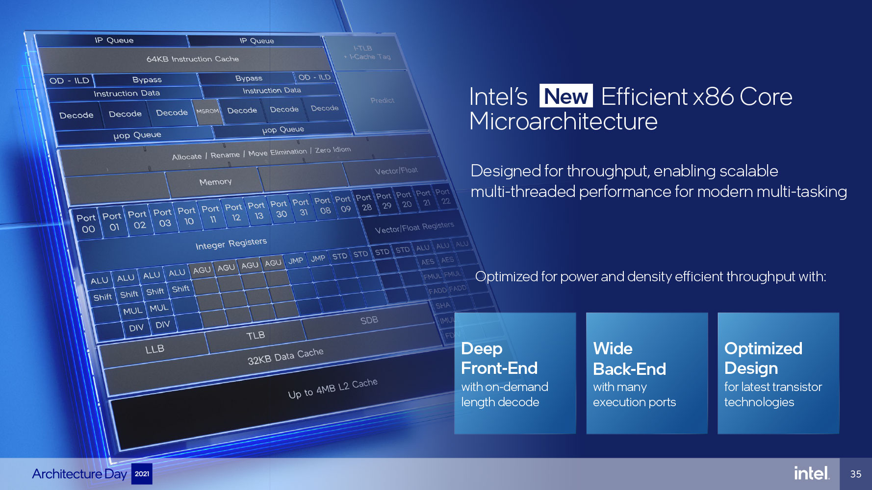
The "Golden Cove" performance core (P-core) features numerical increments to the decode unit, micro-op queue, and micro-op cache. The out-of-order (OoO) engine sees similar increments with 6-wide allocation and 12-wide execution ports, compared to 5-wide allocation and 10-wide execution ports for Cypress Cove. The execution stage sees the addition of a fifth execution port and ALU, FMA with FP16 support, and an updated fast adder (FADD). Similar improvements are made to the cache and memory sub-system. These add toward the 28% IPC uplift for this core. The E-core, on the other hand, is designed to provide a massive performance uplift from the previous-generation "Tremont" low-power microarchitecture, mainly to give it certain ISA capabilities found in larger cores, such as AVX2. The front-end is upgraded by a double-size 64 KB L1 instruction cache, more powerful branch-prediction unit, and two sets of triple out-of-order decoders. The out-of-order engine features a wide 256-entry OoO window and 17 execution ports for more parallelism. The execution stage sees a near 33% increase in both scalar and vector execution stages, as well as double the load store.
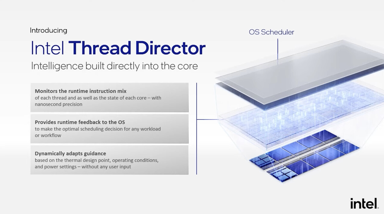

Intel Thread Director is a vital component that ensures the operating system doesn't see "Alder Lake" as having the same kind of CPU cores, sending processing traffic uniformly to all cores. Instead, it gives the OS a degree of awareness of the Hybrid architecture and ensures certain kinds of tasks are allocated exclusively on P-cores and others on E-cores. It also senses the nature of the processing workload, whether it's running in the foreground or background, and decides which kind of cores to tie it to. The OS scheduler by itself moves traffic between cores to meet certain power and thermal objectives, but Thread Director ensures this movement doesn't break the core-type hierarchy. Windows 11 is the recommended version of Windows for Alder Lake as it introduces the ability for software to inform the processor of the nature of its work, and the kind of cores it's comfortable getting processed by.


To eke out the best-possible thermals from the 14 nm node it was stuck with, Intel pulled off some innovative ways to transfer heat between the silicon and cooling solution over the past couple of solutions. These innovations continue with Alder Lake. The die and STIM are now thinner, and the copper IHS thicker. Among the new overclocking capabilities are the ability to tweak even the E-cores, DDR5 memory, new XMP 3.0 profiles for DDR5 memory, synthetic BCLK that ensures a base-clock overclock doesn't break sensitive clock domains that rely on it, and external clock generation, in addition to the processor's internal clock generator.

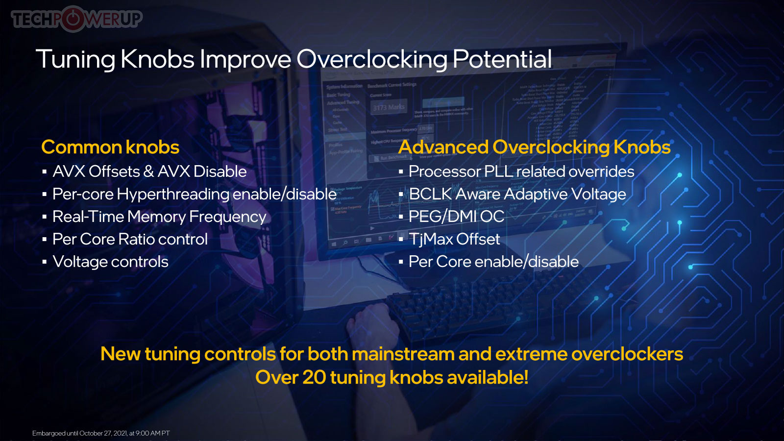
With the monolithic silicon gaining complexity, there are several new overclocking knobs and clock domains to maximize your overclock. The introduction of the E-core adds its own base-clock multiplier, called xE, which works separately from the core ratio of the P-cores, dubbed xP. The xG multiplier dictates iGPU frequency. xR dictates the frequency at which the Ringbus interconnect and L3 cache operate.
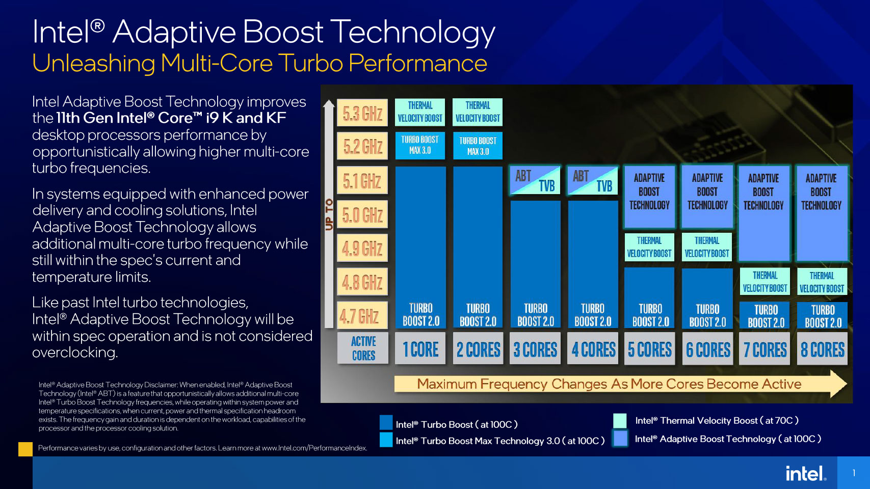
Intel Adaptive Boost Technology (ABT) is a new feature exclusive to the Core i9-12900KS in the 12th Generation, which works to significantly improve multi-threaded performance. To understand ABT, you'll have to understand the three frequency boosting technologies already available to these processors. The i9-12900KS features a nominal clock speed of 3.40 GHz. When all the P-cores are stressed, the chip can afford an all-core boost frequency of 4.80 GHz, provided factors such as the workload being non-AVX, the chip not having exhausted its power level time, etc. Classic Turbo Boost 2.0 drives frequencies up to 5.10 GHz on lighter workloads, for all the cores. Turbo Boost Max 3.0 adds another bin for two of the processor's favored (best-performing) cores, running them at 5.20 GHz. If the cooling performance checks out, Thermal Velocity Boost adds the final 100 MHz to the favored cores, taking the frequency all the way up to 5.30 GHz.
Adaptive Boost is similar to ASUS's "Multi-core Enhancement"—it helps achieve higher clock frequencies when multiple CPU cores are loaded. Unlike the ASUS solution, which is brute-force and static, ABT takes into account not just power limits, thermals, and the cooling efficiency of your machine, but also your motherboard's CPU VRM solution. If the VRM is up for the job, additional power is drawn to elevate all the cores on the processor to higher boost states, improving performance for multi-threaded workloads. The above slide shows you exactly how much clock speed is added. The onus is on the motherboard vendors to design their products such that they can offer ABT, and the motherboard BIOS should report to the processor that its VRM can handle adaptive boosting. What makes ABT special is that it follows the CPU's clock-voltage curve, making it 100% crash-proof—it just works. The price you're paying is higher heat and power consumption. This feature sounds great, and throughout this review, we will test the performance impact of Adaptive Boost.
Intel Z690 Chipset
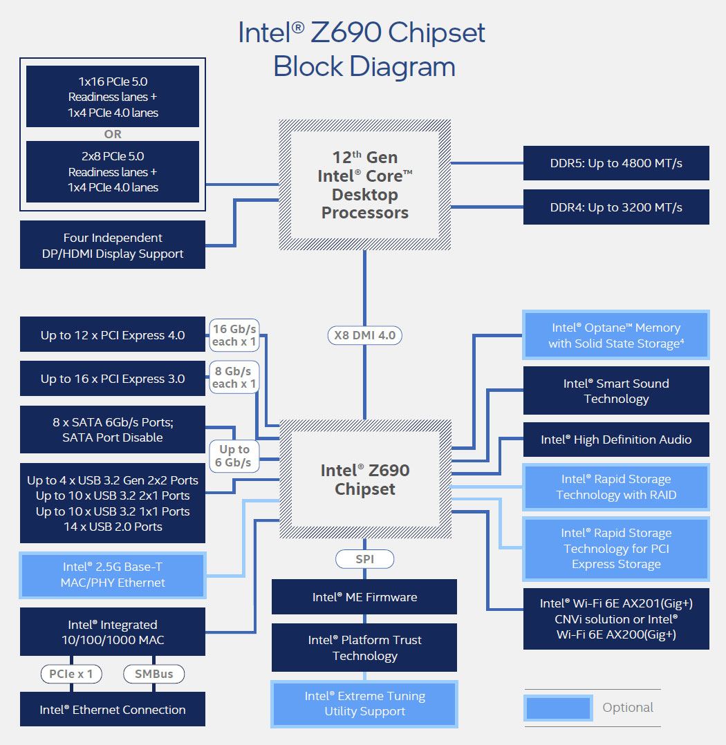
Intel debuted its 12th Gen Core desktop processors in 2021 exclusively with only the unlocked "K" and "KF" variants. As such, it only launched the companion Z690 chipset alongside those. The "locked" processor SKUs and value-ended chipsets joined the product stack in 2022. The Z690 chipset is Intel's first client chipset with PCI-Express 4.0 downstream connectivity. It talks to the "Alder Lake-S" processor over the DMI 4.0 x8 chipset bus. Downstream PCIe connectivity includes 12x Gen 4 and 16x Gen 3 PCIe general-purpose lanes. The rest of its chipset-attached connectivity is the same as Z590, including MIPI SoundWire support, NVMe RAID, 8-port SATA 6 Gbps, and recommended network interfaces that include 2.5 GbE and Wi-Fi 6E.
Intel B660 and H610 Chipsets

As of this writing, VERY few motherboards use the H670 client chipset, making the B660 Intel's mainstream desktop chipset for those with a "locked" 12th Gen Core processor the best option, those who don't need the I/O options of the Z690 and want to save big on the motherboard. The B660 lacks CPU overclocking support, but permits memory overclocking. Motherboard vendors can choose to give it a PCIe Gen 5 PEG slot, as well as DDR5 memory, although you may come across plenty of motherboards with PCIe Gen4 PEG and DDR4 memory. The B660 chipset uses a narrower 4-lane DMI 4.0 chipset bus than what 12th Gen Core processors are capable of (up to 8 DMI 4.0 lanes). This shouldn't be too much of a problem as the chipset only puts out 6 downstream PCIe Gen4 lanes, besides 8 Gen3 lanes. Motherboard designers should use the downstream Gen4 connectivity to wire out another M.2 Gen4 slot. You also get fewer high-bandwidth USB3 port types. The H610 is the bare entry-level chipset. You lose out on memory overclocking, only get Gen3 PCIe connectivity across the board, and have no CPU-attached NVMe.
Jul 5th, 2025 22:59 CDT
change timezone
Latest GPU Drivers
New Forum Posts
- Help Watercooling my PC (8)
- Will you buy a RTX 5090? (627)
- RX 9000 series GPU Owners Club (1128)
- 9800x3d temps (3)
- Last game you purchased? (862)
- TPU's Rosetta Milestones and Daily Pie Thread (2375)
- What are you playing? (23897)
- Folding Pie and Milestones!! (9607)
- Do you game on a handheld console? (98)
- TPU's Nostalgic Hardware Club (20486)
Popular Reviews
- NVIDIA GeForce RTX 5050 8 GB Review
- Fractal Design Scape Review - Debut Done Right
- Crucial T710 2 TB Review - Record-Breaking Gen 5
- ASUS ROG Crosshair X870E Extreme Review
- Sapphire Radeon RX 9060 XT Pulse OC 16 GB Review - An Excellent Choice
- PowerColor ALPHYN AM10 Review
- Upcoming Hardware Launches 2025 (Updated May 2025)
- AMD Ryzen 7 9800X3D Review - The Best Gaming Processor
- Sapphire Radeon RX 9070 XT Nitro+ Review - Beating NVIDIA
- NVIDIA GeForce RTX 5060 8 GB Review
TPU on YouTube
Controversial News Posts
- Intel's Core Ultra 7 265K and 265KF CPUs Dip Below $250 (288)
- NVIDIA Grabs Market Share, AMD Loses Ground, and Intel Disappears in Latest dGPU Update (212)
- Some Intel Nova Lake CPUs Rumored to Challenge AMD's 3D V-Cache in Desktop Gaming (140)
- NVIDIA GeForce RTX 5080 SUPER Could Feature 24 GB Memory, Increased Power Limits (115)
- Microsoft Partners with AMD for Next-gen Xbox Hardware (105)
- NVIDIA Launches GeForce RTX 5050 for Desktops and Laptops, Starts at $249 (105)
- AMD Radeon RX 9070 XT Gains 9% Performance at 1440p with Latest Driver, Beats RTX 5070 Ti (102)
- Intel "Nova Lake‑S" Series: Seven SKUs, Up to 52 Cores and 150 W TDP (100)