 13
13
MSI GeForce RTX 5070 Ti Vanguard SOC Review
(13 Comments) »Introduction
MSI GeForce RTX 5070 Ti Vanguard SOC is the company's fastest and most premium custom design product based on the RTX 5070 Ti. Unlike with the RTX 40-series, there is no SUPRIM series product for the 70 Ti segment, which is a good way to understand MSI's strategy here. The Vanguard brand of graphics card is being introduced with this generation. It incorporates almost all cooling innovations of the SUPRIM, but with more sporty product styling that's designed to look a step up from the Gaming Trio. In a way the Vanguard series is what the Gaming Z series from MSI used to be, a few generations ago. The GeForce RTX 5070 Ti is an upper performance segment graphics card that's on the edge of its segment, teetering on the enthusiast segment. It comes with a starting price of $750, but we know of many custom design cards that are nearing the $1,000-mark, so you might as well consider this enthusiast-class, that is until you see what NVIDIA recommends the RTX 5070 Ti for.

NVIDIA does not explicitly recommend the RTX 5070 Ti as a 4K Ultra HD-class GPU, but something that's designed to more than max out 1440p, perhaps even 21:9 ultrawides, or 1440p high refresh-rate use-cases; although we've known past generations of NVIDIA GPUs in this segment to be fairly capable of 4K Ultra HD gaming, if you can tone down the settings a bit, or use DLSS. The new DLSS 4 technology being introduced with the Blackwell graphics architecture the RTX 5070 Ti is based on, incorporates new Transformer-based AI models that improve image quality at every performance preset of DLSS super resolution, besides the quality of ray-reconstruction and frame generation. Blackwell introduces the exclusive Multi Frame Generation that lets the GPU generate up to 3 frames completely using AI, succeeding a conventionally rendered one, nearly quadrupling framerates.
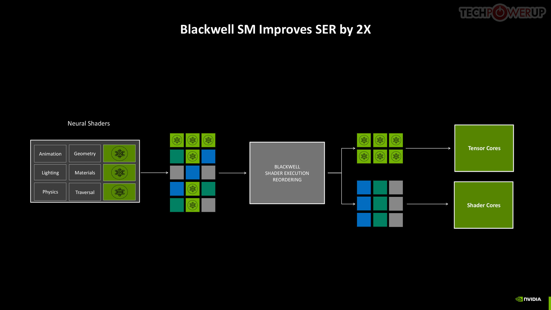
The new Blackwell graphics architecture debuts Neural Rendering a breakthrough new technology that lets generative AI model participate in the core graphics rendering stack, creating objects, textures, and other elements using AI, incorporating it with conventional raster 3D graphics, much in the same way RTX blends ray traced objects with it. This is only possible on Blackwell because of a new hardware scheduling component called the AI Management Processor (AMP), and the significant increases in memory bandwidth that allow the GPU to run AI models and render graphics in tandem. NVIDIA even worked with Microsoft to standardize the technology at the DirectX API level, letting applications directly access the Tensor cores.
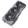
The new Blackwell streaming multiprocessor (SM) features concurrent FP32 and INT32 math capability on all its CUDA cores. The older Ada Lovelace SM only has INT32 capability on half its cores. The shader execution reordering engine is now aware of neural shaders and neural objects, which it can allocate to the Tensor cores. The new 5th Gen Tensor core comes with FP4 data format capability to increase throughput by trading in precision. The 4th Gen RT core comes with even more specialized hardware, including components that enable Mega Geometry, or the ability for ray traced objects to have exponentially higher triangle counts (and the need for rays to interact with all of those triangles).
The GeForce RTX 5070 Ti is based on the same GB203 silicon as the RTX 5080, which it is cut down from, by enabling 70 out of 84 SM present on the silicon. This works out to 8,960 CUDA cores, 280 Tensor cores, 70 RT cores, 280 TMUs, and 96 ROPs. The ROP count is lowered as NVIDIA disabled an entire GPC to achieve the desired SM count. The L2 cache has been lowered, too, down to 48 MB from the 64 MB. The memory sub-system is almost unchanged from the RTX 5080, but is a massive upgrade over the previous generation RTX 4070 Ti. You now get 16 GB of faster 28 Gbps GDDR7 memory across a 256-bit wide memory bus, compared to the 12 GB of 21 Gbps GDDR6X over 192-bit, of the RTX 4070 Ti. This works out to 896 GB/s of memory bandwidth, or a massive 77% increase.
The MSI RTX 5070 Ti Vanguard SOC comes with a slick, premium version of the Tri Frozr cooling solution, which is noticeably heavier than the one the company's RTX 5070 Ti Gaming Trio OC+ comes with (which we also reviewed today). The Vanguard SOC comes with a heavier heatsink that uses a vapor chamber plate, eight heatpipes, and a slightly thicker fin-stack. The StormForce fans are similar to the ones on the Gaming Trio OC+. The cooler shroud and backplate are made of more premium brushed metal 2-tone surfaces. The RTX 5070 Ti Vanguard SOC offers the company's highest factory overclock, with 2588 MHz boost on tap compared to the 2452 MHz reference. We expect the MSI RTX 5070 Ti SOC to be priced at $1000, a 33% premium over the NVIDIA baseline price.
| Price | Cores | ROPs | Core Clock | Boost Clock | Memory Clock | GPU | Transistors | Memory | |
|---|---|---|---|---|---|---|---|---|---|
| RTX 3080 | $420 | 8704 | 96 | 1440 MHz | 1710 MHz | 1188 MHz | GA102 | 28000M | 10 GB, GDDR6X, 320-bit |
| RTX 4070 | $490 | 5888 | 64 | 1920 MHz | 2475 MHz | 1313 MHz | AD104 | 35800M | 12 GB, GDDR6X, 192-bit |
| RX 7800 XT | $440 | 3840 | 96 | 2124 MHz | 2430 MHz | 2425 MHz | Navi 32 | 28100M | 16 GB, GDDR6, 256-bit |
| RX 6900 XT | $450 | 5120 | 128 | 2015 MHz | 2250 MHz | 2000 MHz | Navi 21 | 26800M | 16 GB, GDDR6, 256-bit |
| RX 6950 XT | $630 | 5120 | 128 | 2100 MHz | 2310 MHz | 2250 MHz | Navi 21 | 26800M | 16 GB, GDDR6, 256-bit |
| RTX 3090 | $900 | 10496 | 112 | 1395 MHz | 1695 MHz | 1219 MHz | GA102 | 28000M | 24 GB, GDDR6X, 384-bit |
| RTX 4070 Super | $590 | 7168 | 80 | 1980 MHz | 2475 MHz | 1313 MHz | AD104 | 35800M | 12 GB, GDDR6X, 192-bit |
| RX 7900 GRE | $530 | 5120 | 160 | 1880 MHz | 2245 MHz | 2250 MHz | Navi 31 | 57700M | 16 GB, GDDR6, 256-bit |
| RTX 4070 Ti | $700 | 7680 | 80 | 2310 MHz | 2610 MHz | 1313 MHz | AD104 | 35800M | 12 GB, GDDR6X, 192-bit |
| RTX 4070 Ti Super | $750 | 8448 | 112 | 2340 MHz | 2610 MHz | 1313 MHz | AD103 | 45900M | 16 GB, GDDR6X, 256-bit |
| RX 7900 XT | $620 | 5376 | 192 | 2000 MHz | 2400 MHz | 2500 MHz | Navi 31 | 57700M | 20 GB, GDDR6, 320-bit |
| RTX 3090 Ti | $1000 | 10752 | 112 | 1560 MHz | 1950 MHz | 1313 MHz | GA102 | 28000M | 24 GB, GDDR6X, 384-bit |
| RTX 4080 | $940 | 9728 | 112 | 2205 MHz | 2505 MHz | 1400 MHz | AD103 | 45900M | 16 GB, GDDR6X, 256-bit |
| RTX 4080 Super | $990 | 10240 | 112 | 2295 MHz | 2550 MHz | 1438 MHz | AD103 | 45900M | 16 GB, GDDR6X, 256-bit |
| RX 7900 XTX | $820 | 6144 | 192 | 2300 MHz | 2500 MHz | 2500 MHz | Navi 31 | 57700M | 24 GB, GDDR6, 384-bit |
| RTX 5070 Ti | $750 | 8960 | 96 | 2295 MHz | 2452 MHz | 1750 MHz | GB203 | 45600M | 16 GB, GDDR7, 256-bit |
| MSI RTX 5070 Ti Vanguard SOC | $1000 | 8960 | 96 | 2295 MHz | 2588 MHz (+136 MHz) | 1750 MHz | GB203 | 45600M | 16 GB, GDDR7, 256-bit |
| RTX 5080 | $1000 | 10752 | 112 | 2295 MHz | 2617 MHz | 1875 MHz | GB203 | 45600M | 16 GB, GDDR7, 256-bit |
| RTX 4090 | $2400 | 16384 | 176 | 2235 MHz | 2520 MHz | 1313 MHz | AD102 | 76300M | 24 GB, GDDR6X, 384-bit |
| RTX 5090 | $2000 | 21760 | 176 | 2017 MHz | 2407 MHz | 1750 MHz | GB202 | 92200M | 32 GB, GDDR7, 512-bit |
NVIDIA Blackwell Architecture

NVIDIA does not provide a block diagram for the GB203 GPU (we asked), so we had to quickly hack one out from the GB202 diagram. This is accurate just not as pretty.
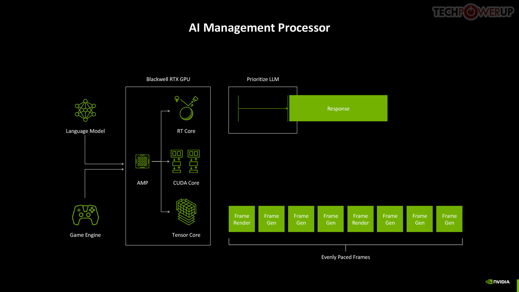
The GeForce Blackwell graphics architecture heralds NVIDIA's 4th generation of RTX, the late-2010s re-invention of the modern GPU that sees a fusion of real time ray traced objects with conventional raster 3D graphics. With Blackwell, NVIDIA is helping add another dimension, neural rendering, the ability for the GPU to leverage a generative AI to create portions of a frame. This is different from DLSS, where an AI model is used to reconstruct details in an upscaled frame based on its training date, temporal frames, and motion vectors. Today we are reviewing the RTX 5070 Ti. At the heart of this graphics card is the new 5 nm GB203 silicon, the same chip that powers the RTX 5080. This chip has very similar die size and transistor counts to the previous generation AD103 powering the RTX 4080, because both chips are built on the exact same process—TSMC's "NVIDIA 4N", or 5 nm EUV with NVIDIA-specific characteristics—but is based on the newer Blackwell graphics architecture. The GB203 measures 378 mm² in die-area and rocks 45.6 billion transistors (compared to the 378.6 mm² die-area and 45.9 billion transistors of the AD103). This is where the similarities end.
The GB203 silicon is laid out essentially in the same component hierarchy as past generations of NVIDIA GPUs, but with a few notable changes. The GPU features a PCI-Express 5.0 x16 host interface. PCIe Gen 5 has been around since Intel's 12th Gen Core "Alder Lake" and AMD's Ryzen 7000 "Zen 4," so there is a sizable install-base of systems that can take advantage of it. The GPU is of course compatible with older generations of PCIe. The GB203 also features the new GDDR7 memory interface that's making its debut with this generation. The chip features a 256-bit wide memory bus, which is half the bus width of the GB202 powering the RTX 5090. NVIDIA is using this to drive 16 GB of memory at 30 Gbps speeds, yielding 960 GB/s of memory bandwidth, which is a 34% increase over the RTX 4080 and its 22.5 Gbps GDDR6X.
The GigaThread Engine is the main graphics rendering workload allocation logic on the GB203, but there's a new addition, a dedicated serial processor for managing all AI acceleration resources on the GPU, NVIDIA calls this AMP (AI management processor). Other components at the global level are the Optical Flow Processor, a component involved in older versions of DLSS frame generation and for video encoding; and an updated media acceleration engine consisting of two NVENC encode accelerators, and two NVDEC decode accelerators. On the RTX 5070 Ti, one of these two NVDEC units is disabled. The new 9th Gen NVENC video encode accelerators come with 4:2:2 AV1 and HEVC encoding support. The central region of the GPU has the single largest common component, the 64 MB L2 cache. The RTX 5070 Ti is configured with 48 MB of this cache.


Each graphics processing cluster (GPC) is a subdivision of the GPU with nearly all components needed for graphics rendering. On the GB203, a GPC consists of 12 streaming multiprocessors (SM) across 6 texture processing clusters (TPCs), and a raster engine consisting of 16 ROPs. Each SM contains 128 CUDA cores. Unlike the Ada generation SM that each had 64 FP32+INT32 and 64 purely-FP32 SIMD units, the new Blackwell generation SM features concurrent FP32+INT32 capability on all 128 SIMD units. These 128 CUDA cores are arranged in four slices, each with a register file, a level-0 instruction cache, a warp scheduler, two sets of load-store units, and a special function unit (SFU) handling some special math functions such as trigonometry, exponents, logarithms, reciprocals, and square-root. The four slices share a 128 KB L1 data cache, and four TMUs. The most exotic components of the Blackwell SM are the four 5th Gen Tensor cores, and a 4th Gen RT core. The RTX 5070 Ti is carved out from the GB203 by disabling an entire GPC, plus one TPC from the remaining six GPCs, resulting in 70 SM. You hence end up with 8,960 CUDA cores, 280 Tensor cores, 70 RT cores, 280 TMUs, and 96 ROPs.

Perhaps the biggest change to the way the SM handles work introduced with Blackwell is the concept of neural shaders—treating portions of the graphics rendering workload done by a generative AI model as shaders. Microsoft has laid the groundwork for standardization of neural shaders with its Cooperative Vectors API, in the latest update to DirectX 12. The Tensor cores are now accessible for workloads through neural shaders, and the shader execution reordering (SER) engine of the Blackwell SM is able to more accurately reorder workloads for the CUDA cores and the Tensor core in an SM.

The new 5th Gen Tensor core introduces support for FP4 data format (1/8 precision) to fast moving atomic workloads, providing 32 times the throughput of the very first Tensor core introduced with the Volta architecture. Over the generations, AI models leveraged lesser precision data formats, and sparsity, to improve performance. The AI management processor (AMP) is what enables simultaneous AI and graphics workloads at the highest levels of the GPU, so it could be simultaneously rendering real time graphics for a game, while running an LLM, without either affecting the performance of the other. AMP is a specialized hardware scheduler for all the AI acceleration resources on the silicon. This plays a crucial role for DLSS 4 multi-frame generation to work.


The 4th Gen RT core not just offers a generational increase in ray testing and ray intersection performance, which lowers the performance cost of enabling path tracing and ray traced effects; but also offers a potential generational leap in performance with the introduction of Mega Geometry. This allows for ray traced objects with extremely high polygon counts, increasing their detail. Poly count and ray tracing present linear increases in performance costs, as each triangle has to intersect with a ray, and there should be sufficient rays to intersect with each of them. This is achieved by adopting clusters of triangles in an object as first-class primitives, and cluster-level acceleration structures. The new RT cores introduce a component called a triangle cluster intersection engine, designed specifically for handling mega geometry. The integration of a triangle cluster compression format and a lossless decompression engine allows for more efficient processing of complex geometry.


The GB203 and the rest of the GeForce Blackwell GPU family is built on the exact same TSMC "NVIDIA 4N" foundry node, which is actually 5 nm, as previous-generation Ada, so NVIDIA directed efforts to finding innovative new ways to manage power and thermals. This is done through a re-architected power management engine that relies on clock gating, power gating, and rail gating of the individual GPCs and other top-level components. It also worked on the speed at which the GPU makes power-related decisions.

The quickest way to drop power is by adjusting the GPU clock speed, and with Blackwell, NVIDIA introduced a means for rapid clock adjustments at the SM-level.

NVIDIA updated both the display engine and the media engine of Blackwell over the previous generation Ada, which drew some flack for holding on to older display I/O standards such as DisplayPort 1.4, while AMD and Intel had moved on to DisplayPort 2.1. The good news is that Blackwell supports DP 2.1 with UHBR20, enabling 8K 60 Hz with a single cable. The company also updated NVDEC and NVENC, which now support AV1 UHQ, double the H.264 decode performance, MV-HEVC, and 4:2:2 formats.
Neural Rendering
Neural Rendering promises to be as transformative to modern graphics as programmable shaders itself. 3D Graphics rendering evolved from fixed-function over the turn of the century, to programmable shaders, HLSL, geometry shaders, compute shaders, and ray tracing, over the past couple of decades. In 2025, NVIDIA is writing the next chapter in this journey with Blackwell neural shaders. This allows for a host of neural-driven effects, including neural materials, neural volumes, and even neural radiance fields. Microsoft introduced the new Cooperative Vectors API for DirectX in a recent update, making it possible to access Tensor cores within a graphics API. Combined with a new shading language, Slang, this breakthrough enables developers to integrate neural techniques directly into their workflows, potentially replacing parts of the traditional graphics pipeline. Slang splits large, complex functions into smaller pieces that are easier to handle. Given that this is a DirectX standard API feature, there is nothing that stops AMD and Intel from integrating Neural Rendering (Cooperative Vectors) into their graphics drivers.
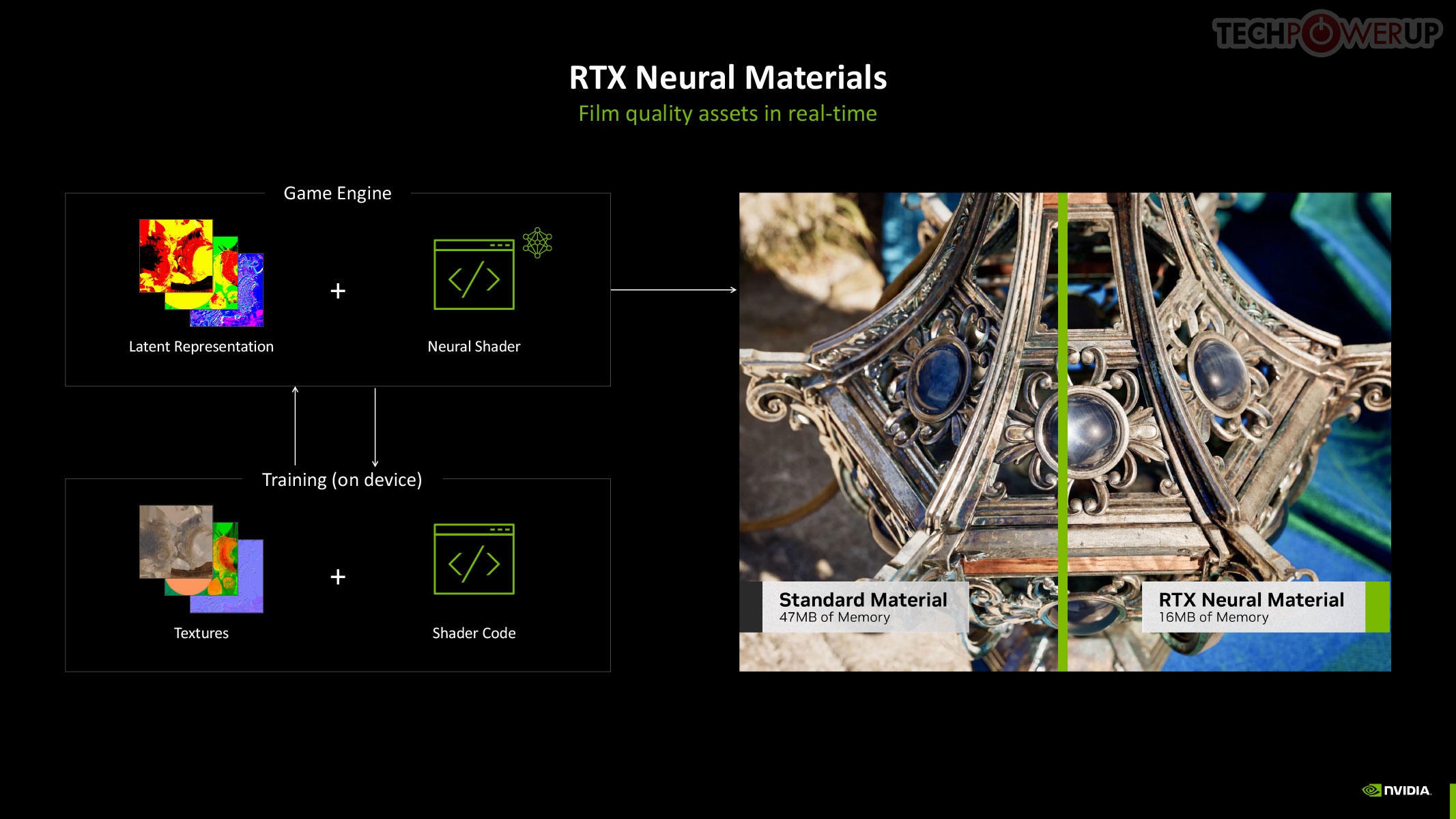
RTX Neural Materials works to significantly reduce the memory footprint of materials in 3D scenes. Under conventional rendering, the memory footprint of a material is bloated from complex shader code. Neural materials convert shader code and texture layers into a compressed neural representation. This results in up to a 7:1 compression ratio and enables small neural networks to generate stunning, film-like materials in real-time. For example, silk rendered with traditional shaders might lack the multicolored sheen seen in real life. Neural materials, however, capture intricate details like color variation and reflections, bringing such surfaces to life with unparalleled realism—and at a fraction of the memory cost.
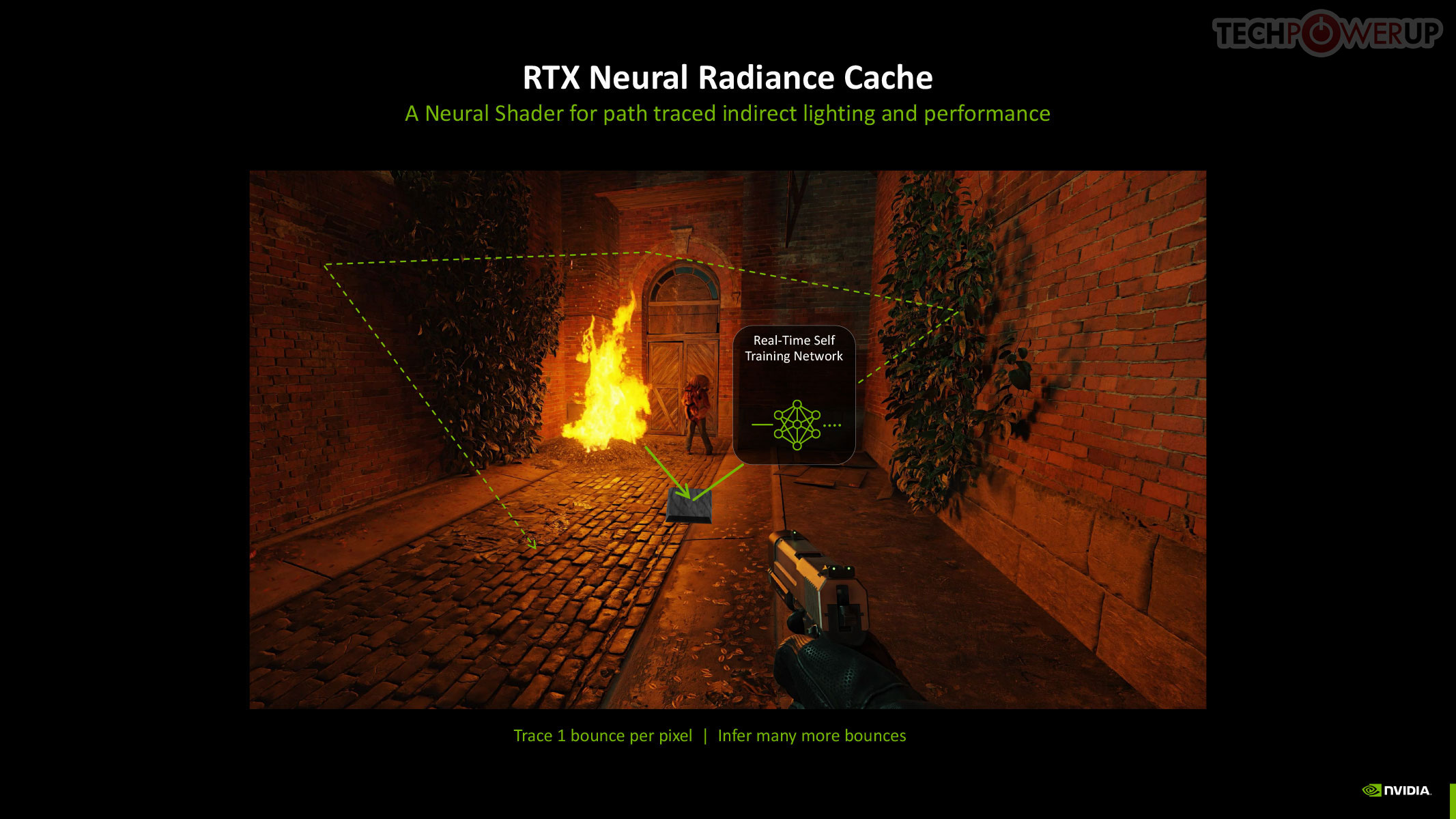
The new Neural Radiance Cache, which dynamically trains a neural network during gameplay using the user's GPU, allowing light transport to be cached spatially, enabling near-infinite light bounces in a scene. This results in realistic indirect lighting and shadows with minimal performance impact. NRC partially traces 1 or 2 rays before storing them in a radiance cache, and infers an infinite amount of rays and bounces for a more accurate representation of indirect lighting in the game scene.
DLSS 4 and Multi Frame Generation
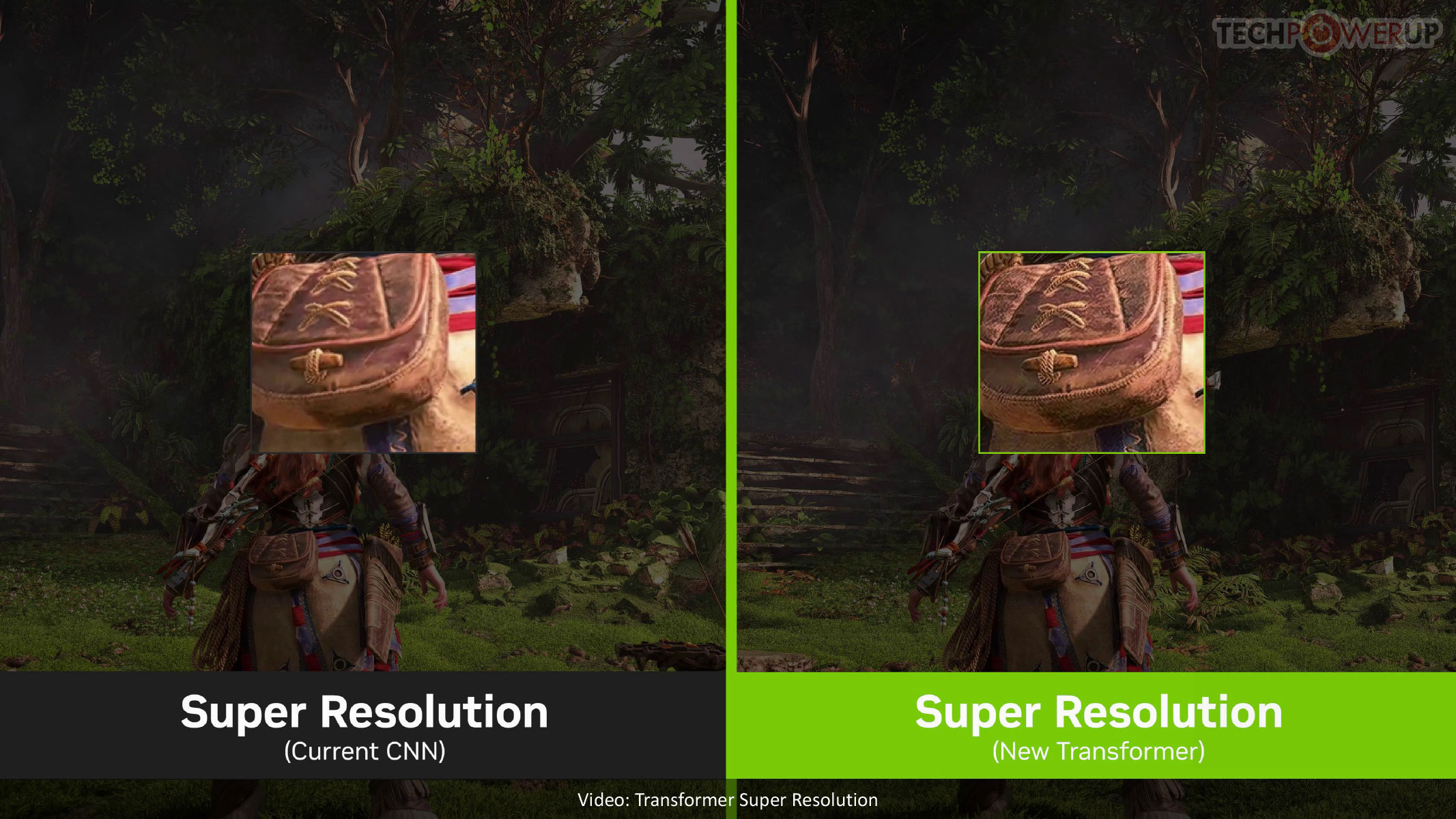
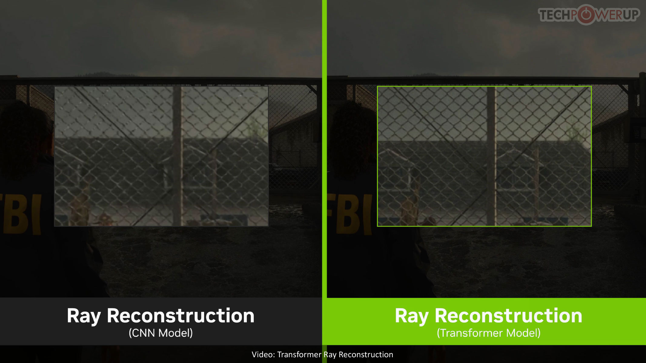
DLSS 4 introduces a major leap in image quality and performance. It isn't just a version bump with the introduction of a new feature, namely Multi Frame Generation, but introduces updates to nearly all DLSS sub-features. DLSS from its very beginning relied on AI to reconstruct details in super resolution, and with DLSS 4, NVIDIA is introducing a new transformer-based AI model to succeed the convolutional neural networks previous used, for double the parameters, four times the compute performance, and significantly improved image quality. Ray Reconstruction, introduced with DLSS 3.5, gets a significant image quality update with the new transformer-based model.
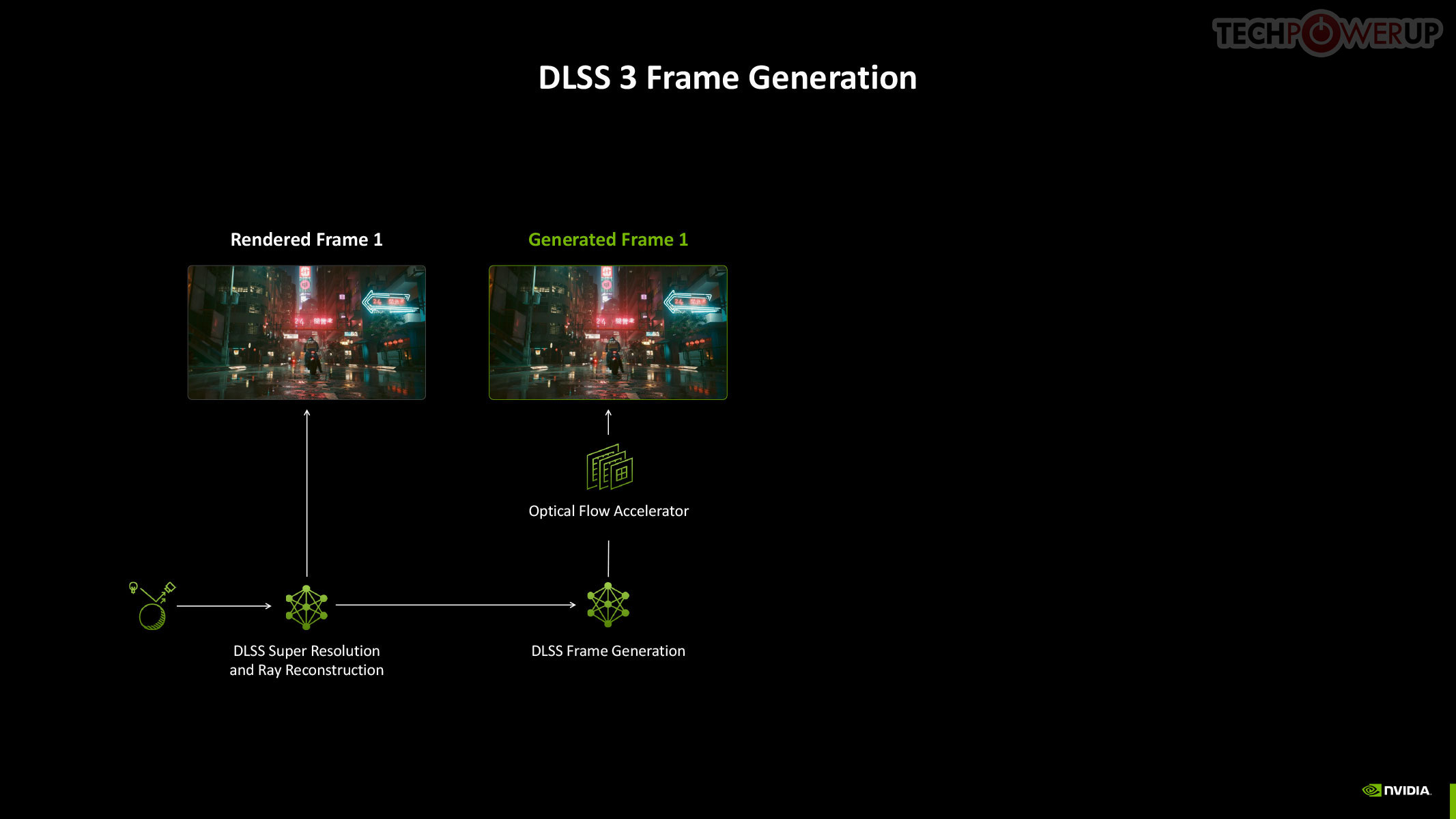
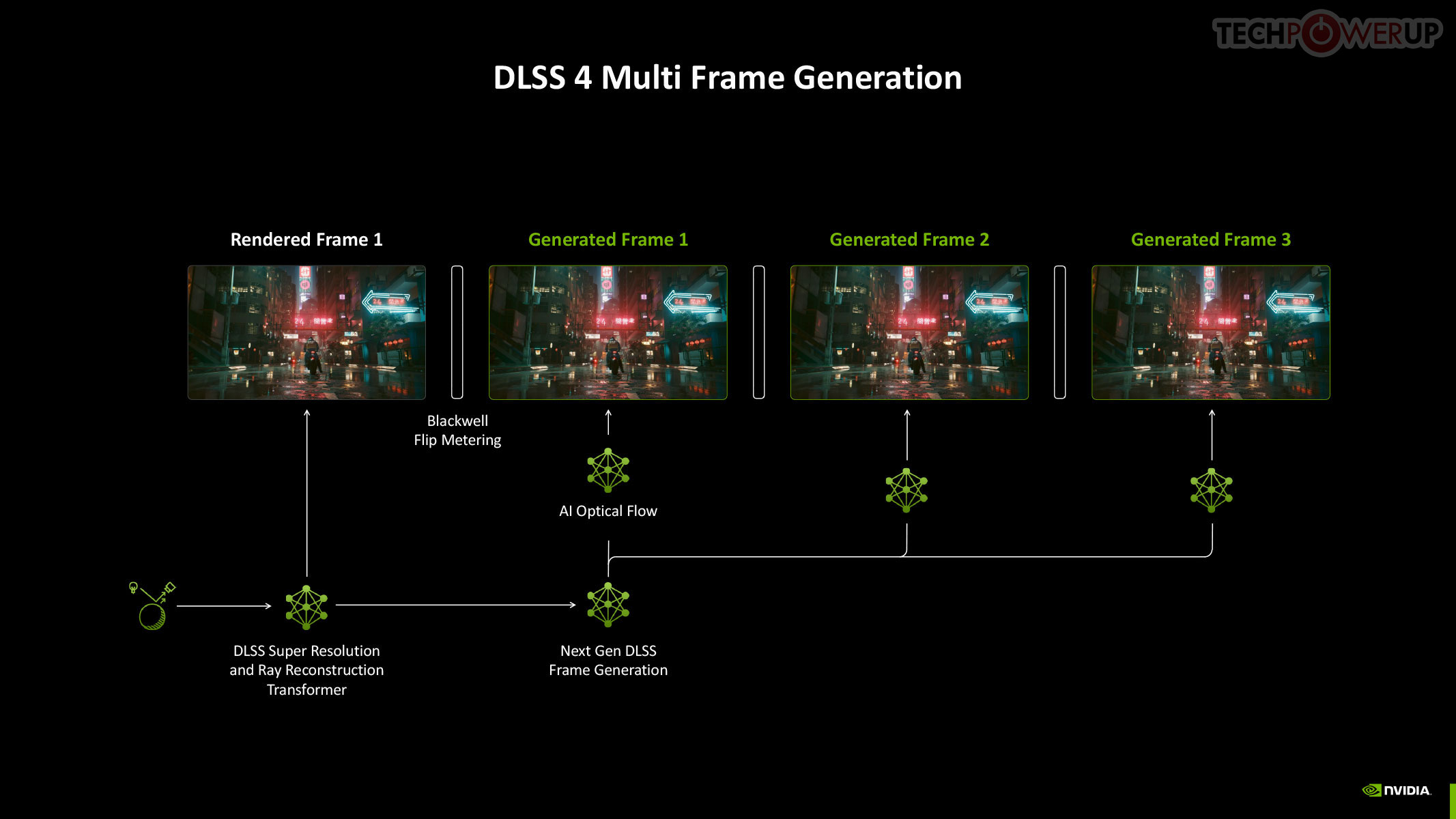
To understand Multi Frame Generation, you need to understand how DLSS Frame Generation, introduced with GeForce Ada, works. An Optical Flow Accelerator component gives the DLSS algorithm data to generate an entire frame using a neural network, using information from a previous rendered frame, effectively doubling frame rate. In Multi Frame Generation, AI takes over the functions of optical flow, to predict up to three frames following a conventionally rendered frame, effectively drawing four frames form the rendering effort of one.

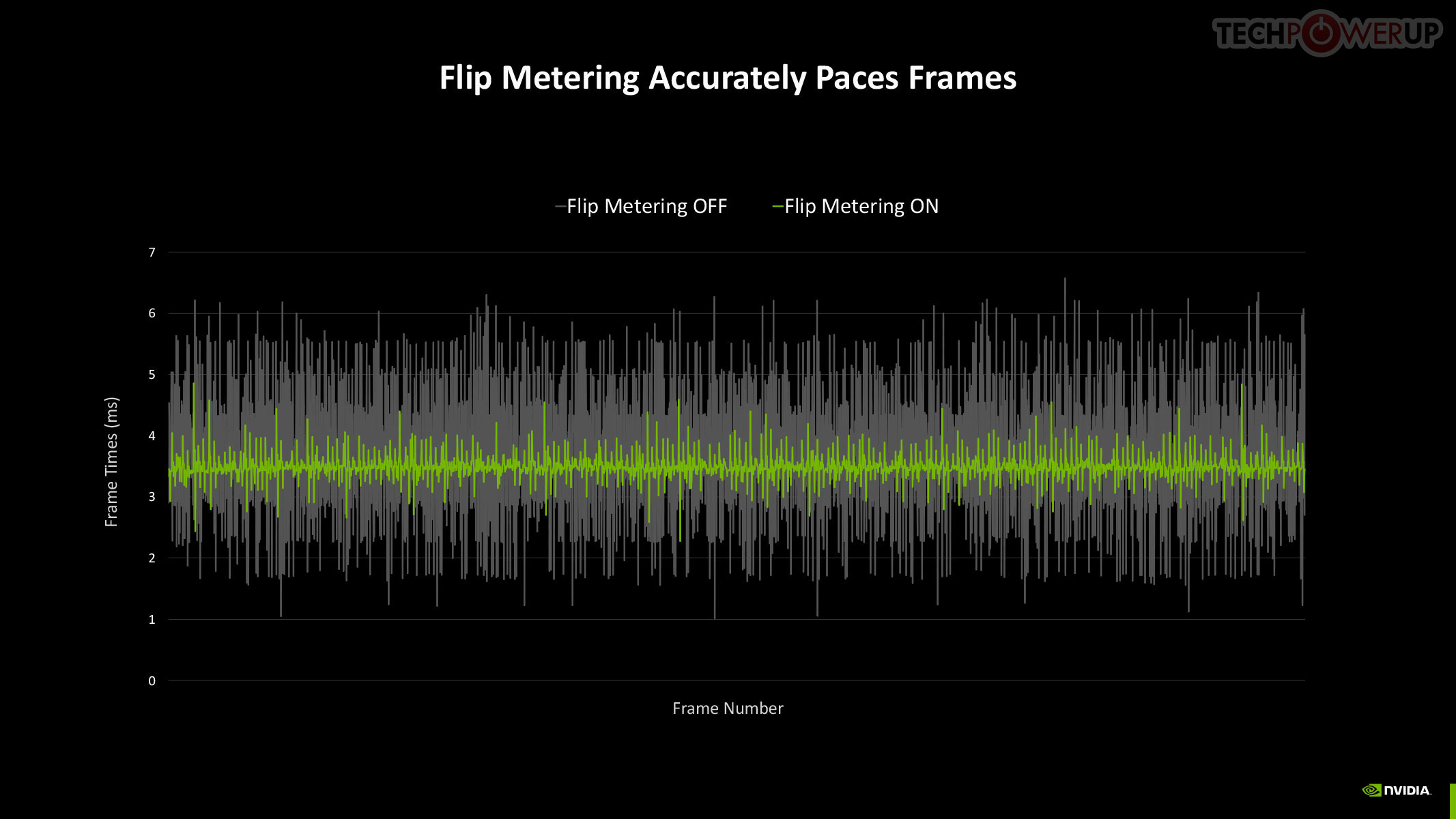
Now, assuming this rendered frame is a product of Super Resolution, with the maximum performance setting generating 4x the pixels from a single rendered pixel, you're looking at a possibility where the rendering effort of 1/4th a frame goes into drawing 4 frames, or 15 in every 16 pixels being generated entirely by DLSS. When generating so many frames, Frame Pacing becomes a problem—irregular frame intervals impact smoothness. DLSS 4 addresses these issues by using a dedicated hardware unit inside Blackwell, which takes care of flip metering, reducing frame display variability by 5-10x. The Display Engine of Blackwell contains the hardware for flip metering.
NVIDIA Reflex 2
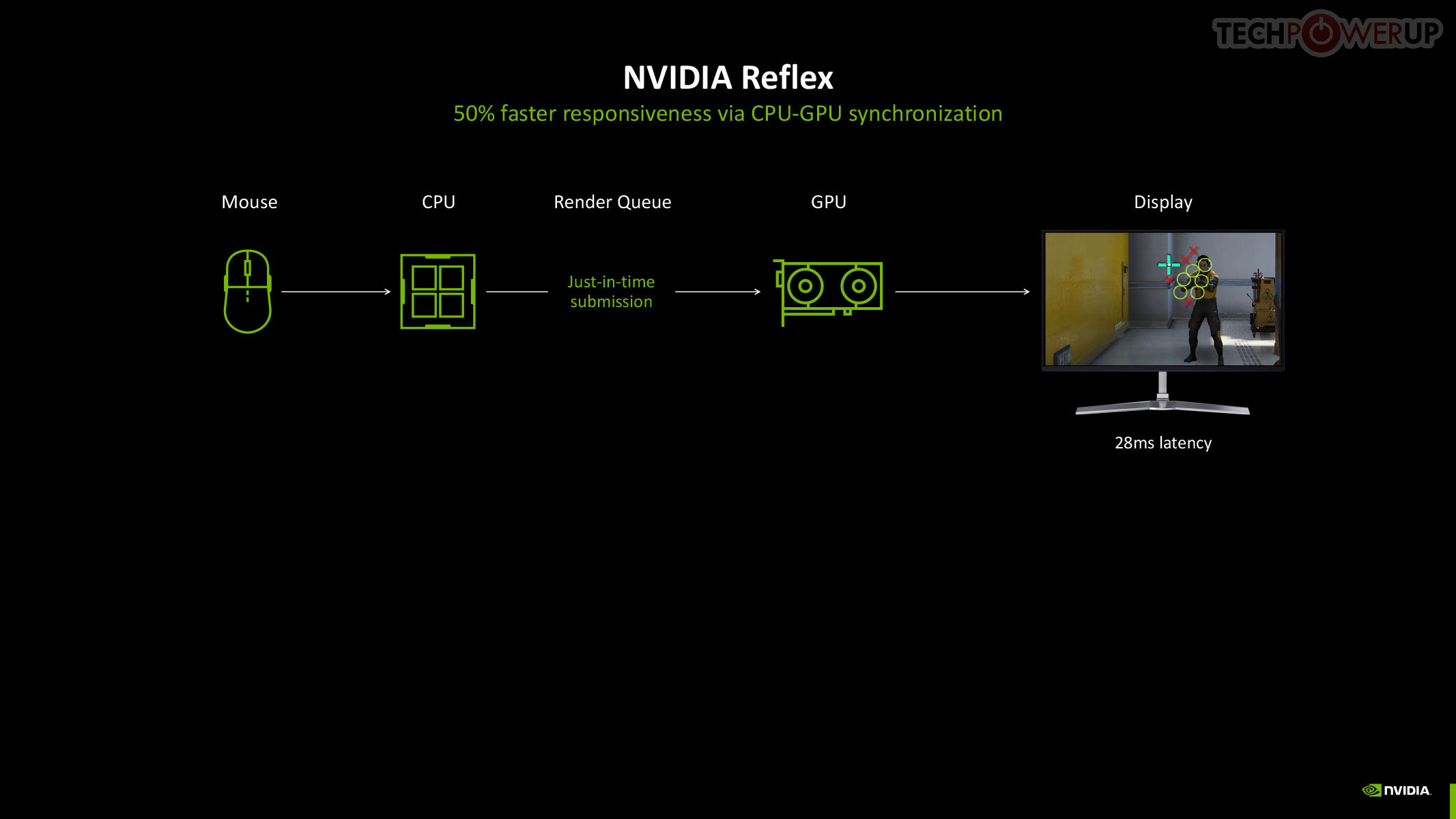
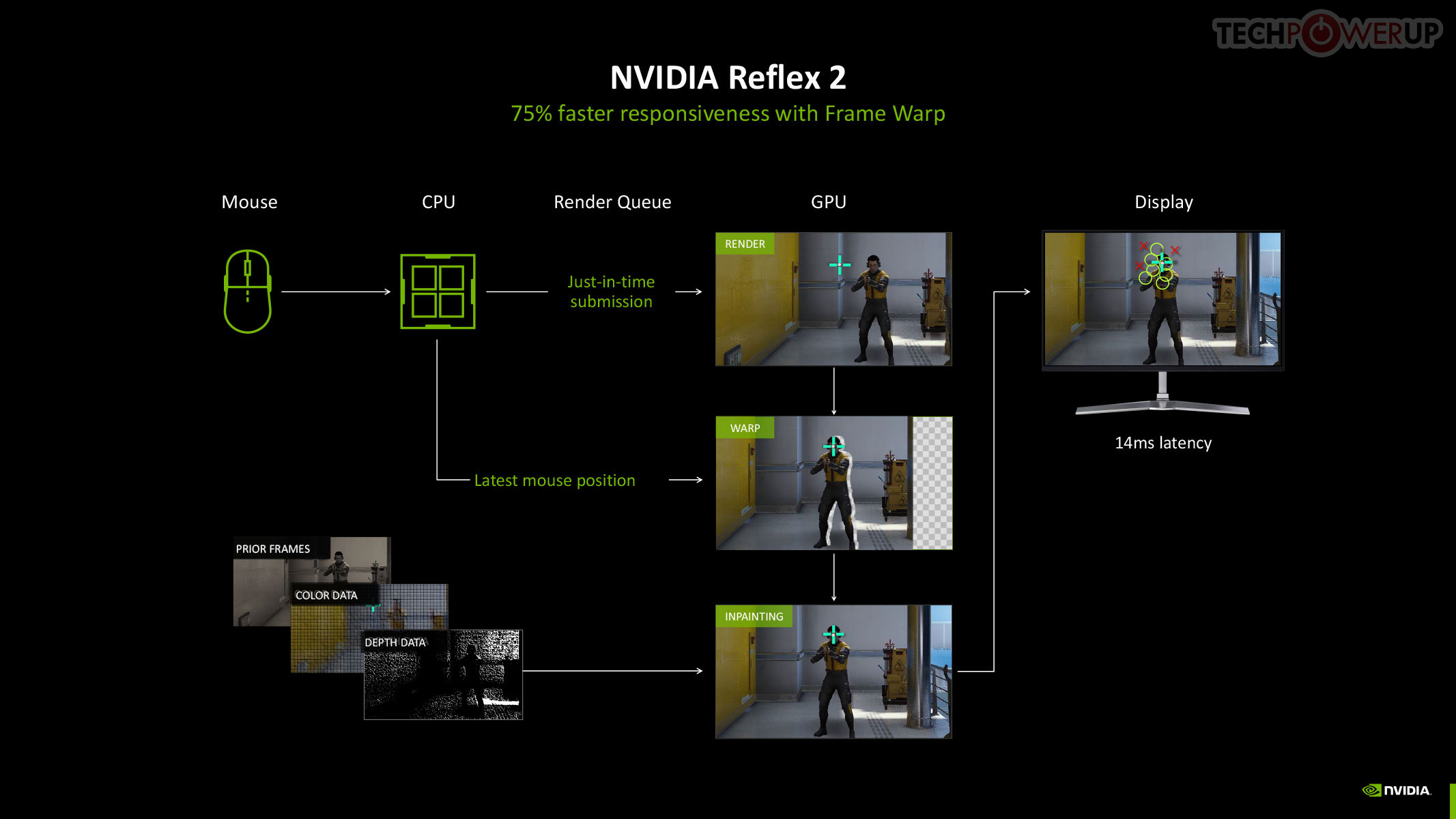
The original NVIDIA Reflex brought about a significant improvement to the responsiveness of maxed out graphics in competitive online gameplay, by compacting the rendering queue with the goal of reducing the whole system latency by up to 50%. Reflex is mandatory in DLSS 3 Frame Generation, given the latency cost imposed by the technology. Multi-frame generation calls for an equally savvy piece of technology, so we hence have Reflex 2. NVIDIA claims to have achieved a 75% reduction in latency with Frame Warp, which updates the camera (viewport) positions based on user inputs in real-time, and then uses temporal information to reconstruct the frame to display.
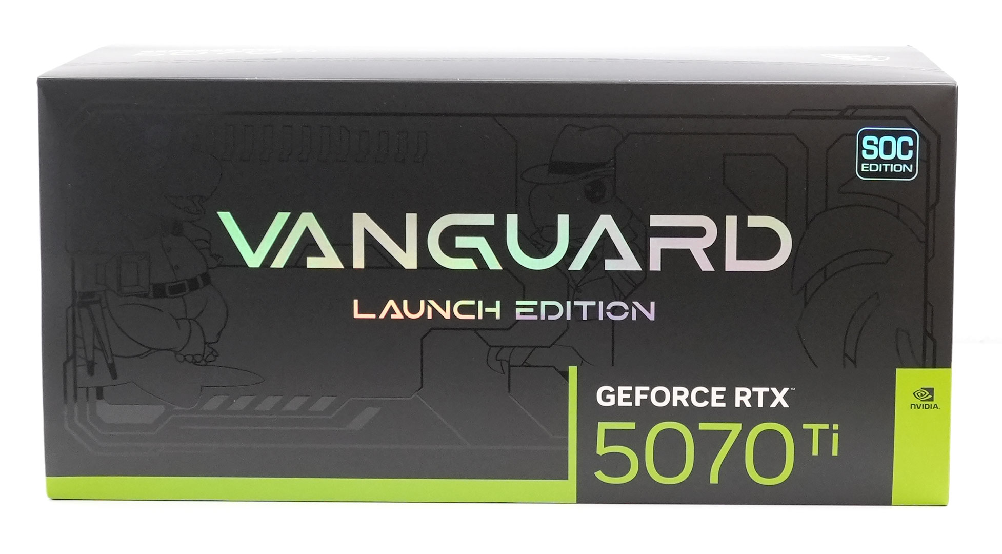
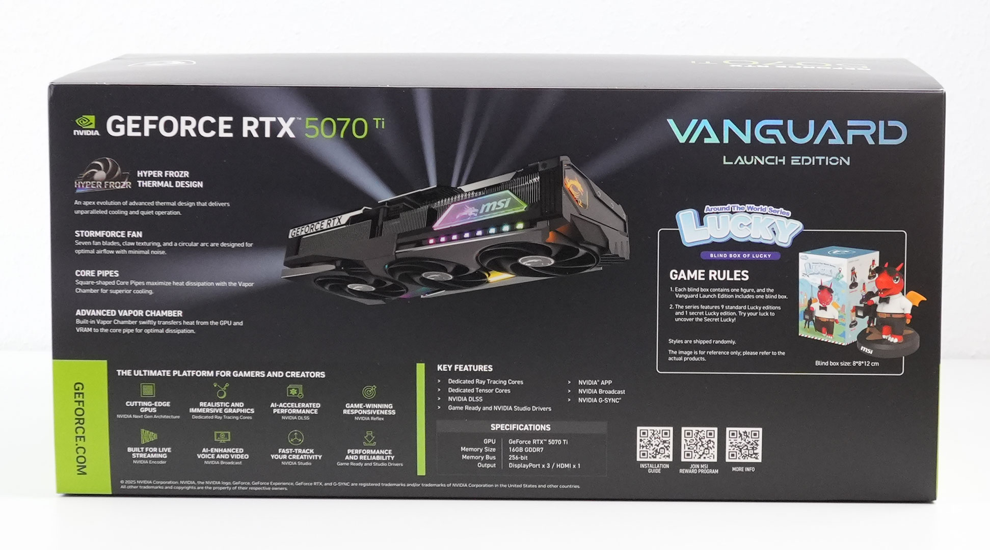
Packaging
The Card
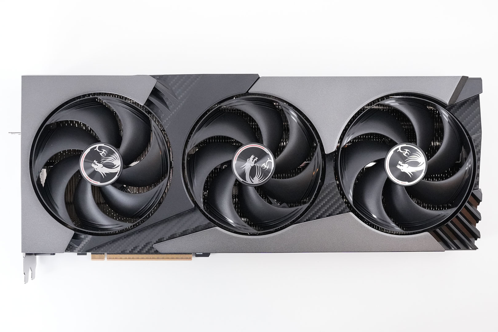
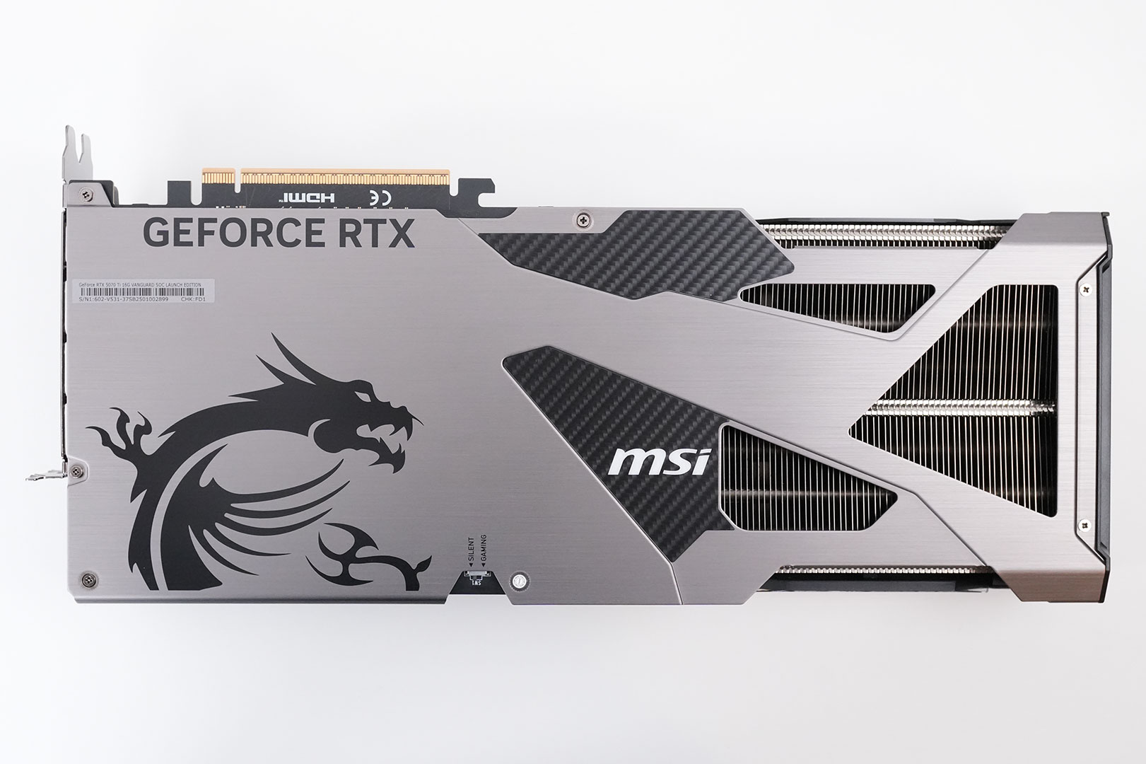
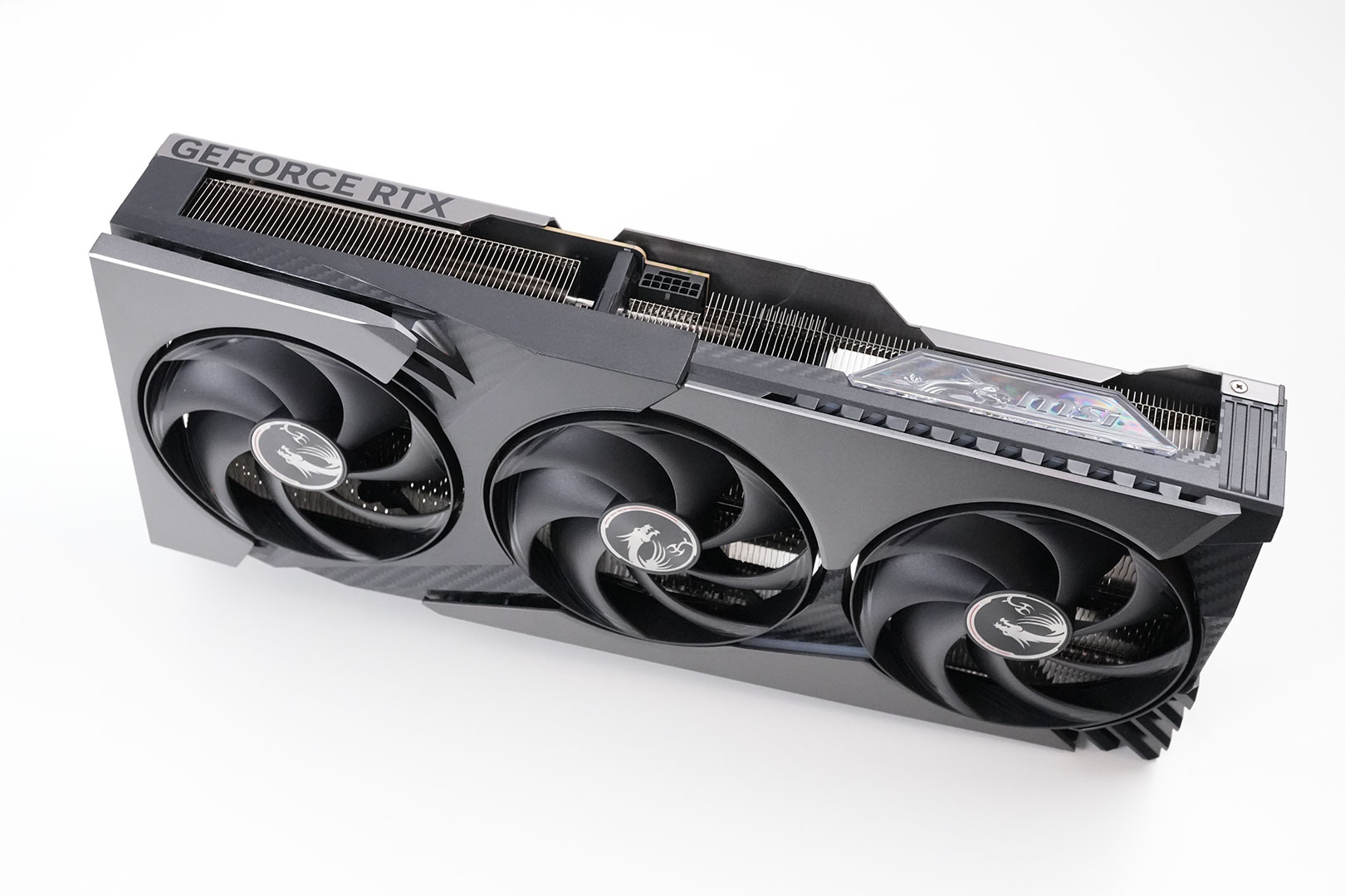
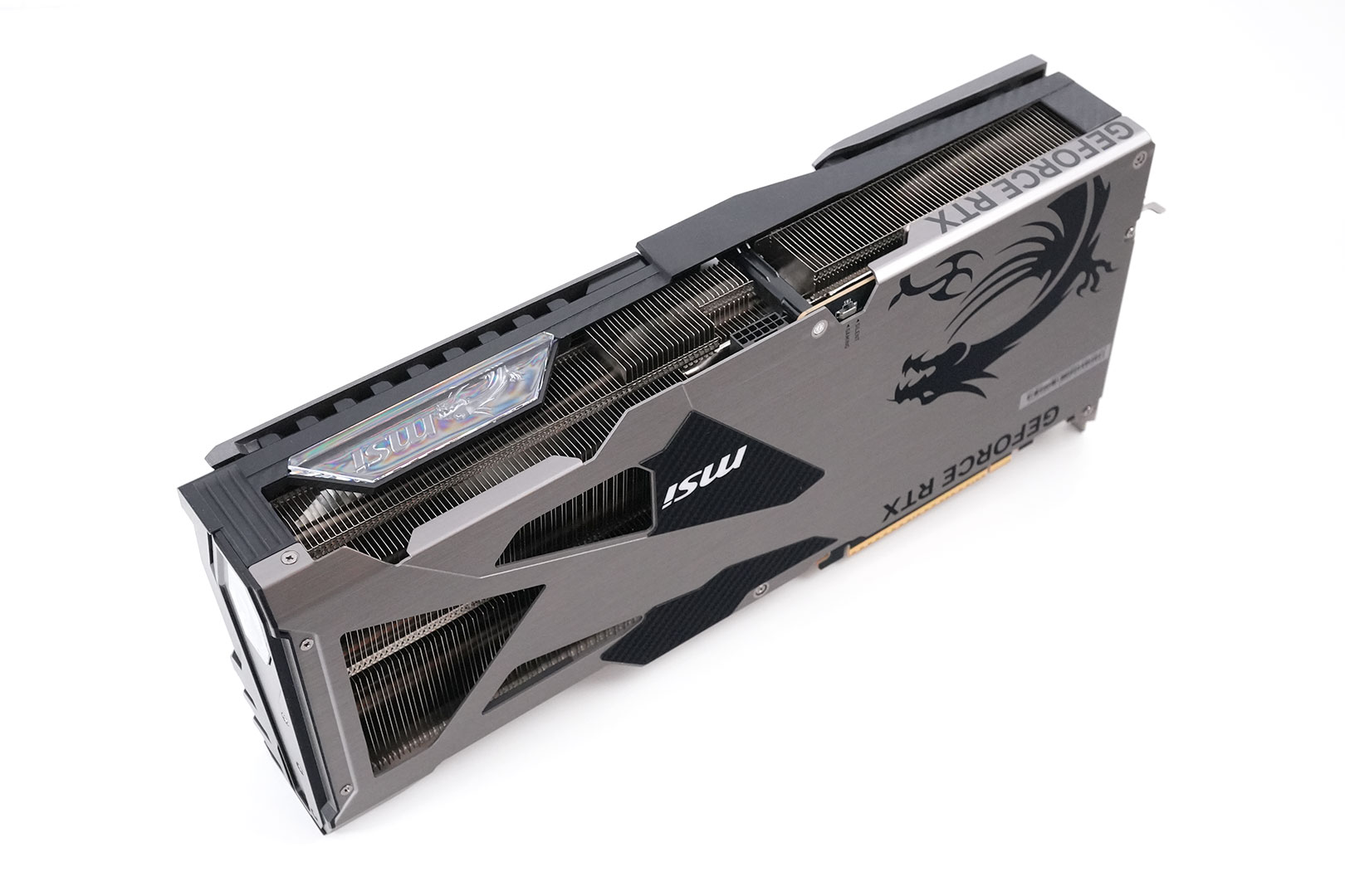
Vanguard is MSI's new GPU lineup and the cards are looking good. The color theme is still metal, with highlights in various shades of gray, but the color theme is a bit darker than Suprim—I like. On the back you get a metal backplate with a large cutout.
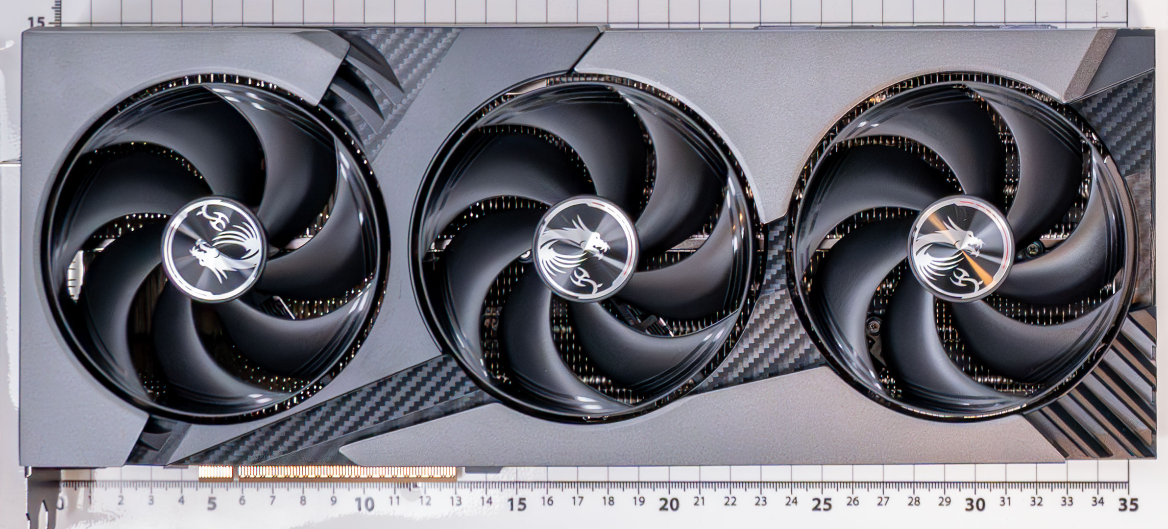
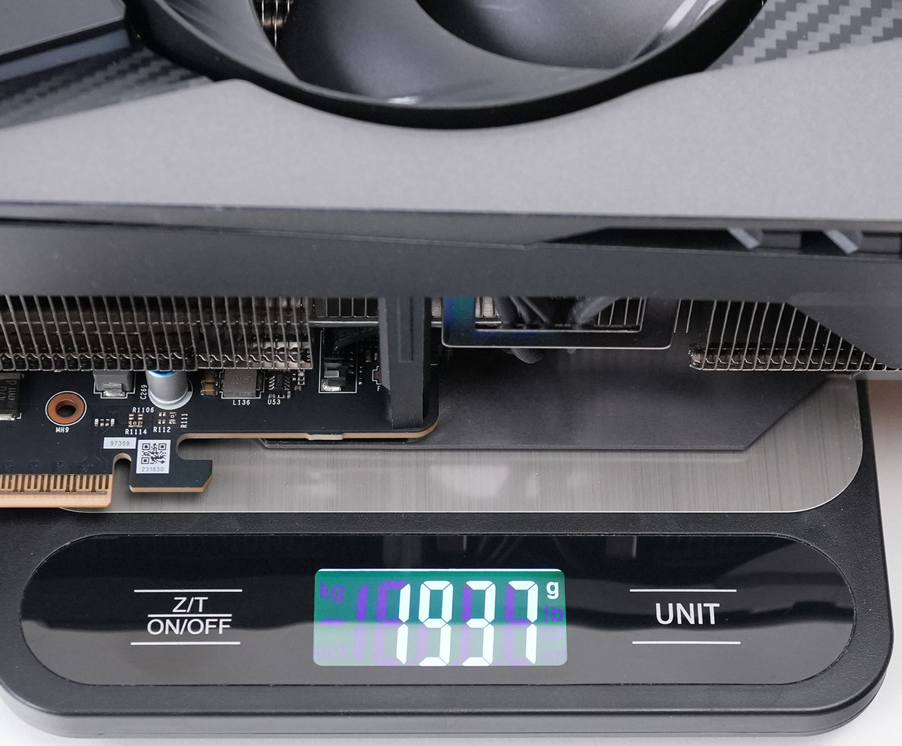
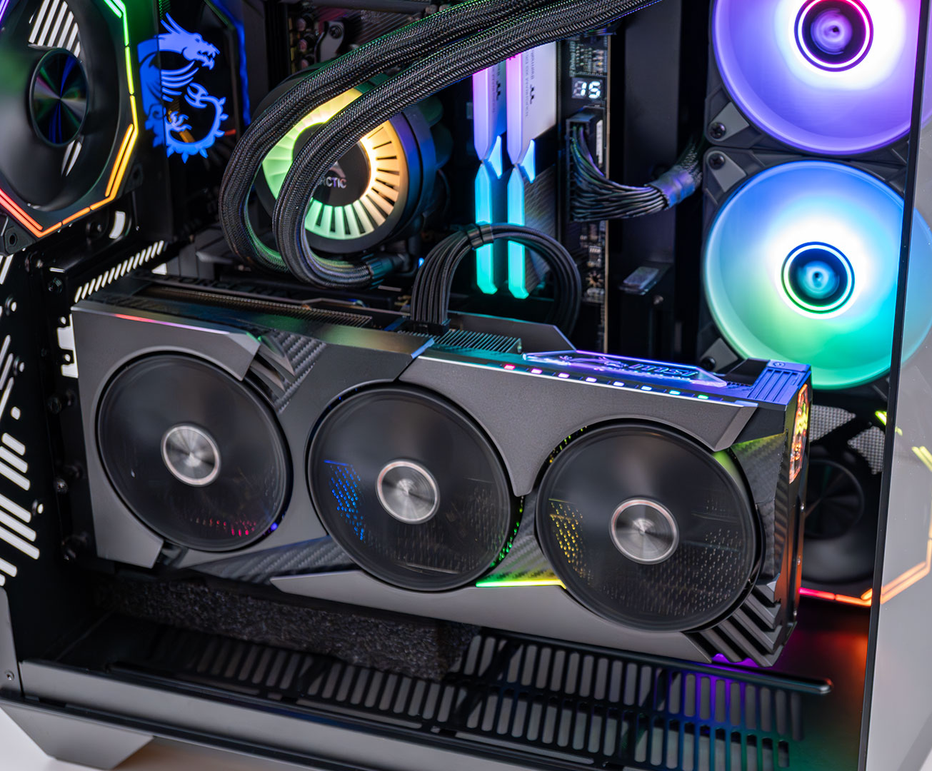
Dimensions of the card are 36.0 x 15.0 cm, and it weighs 1937 g.
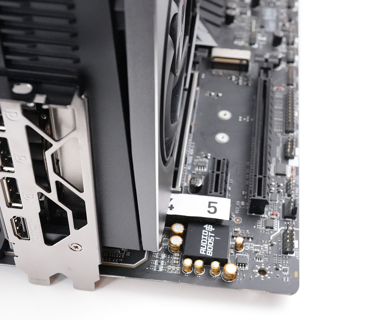
Installation requires four slots in your system. We measured the card's width to be 66 mm.
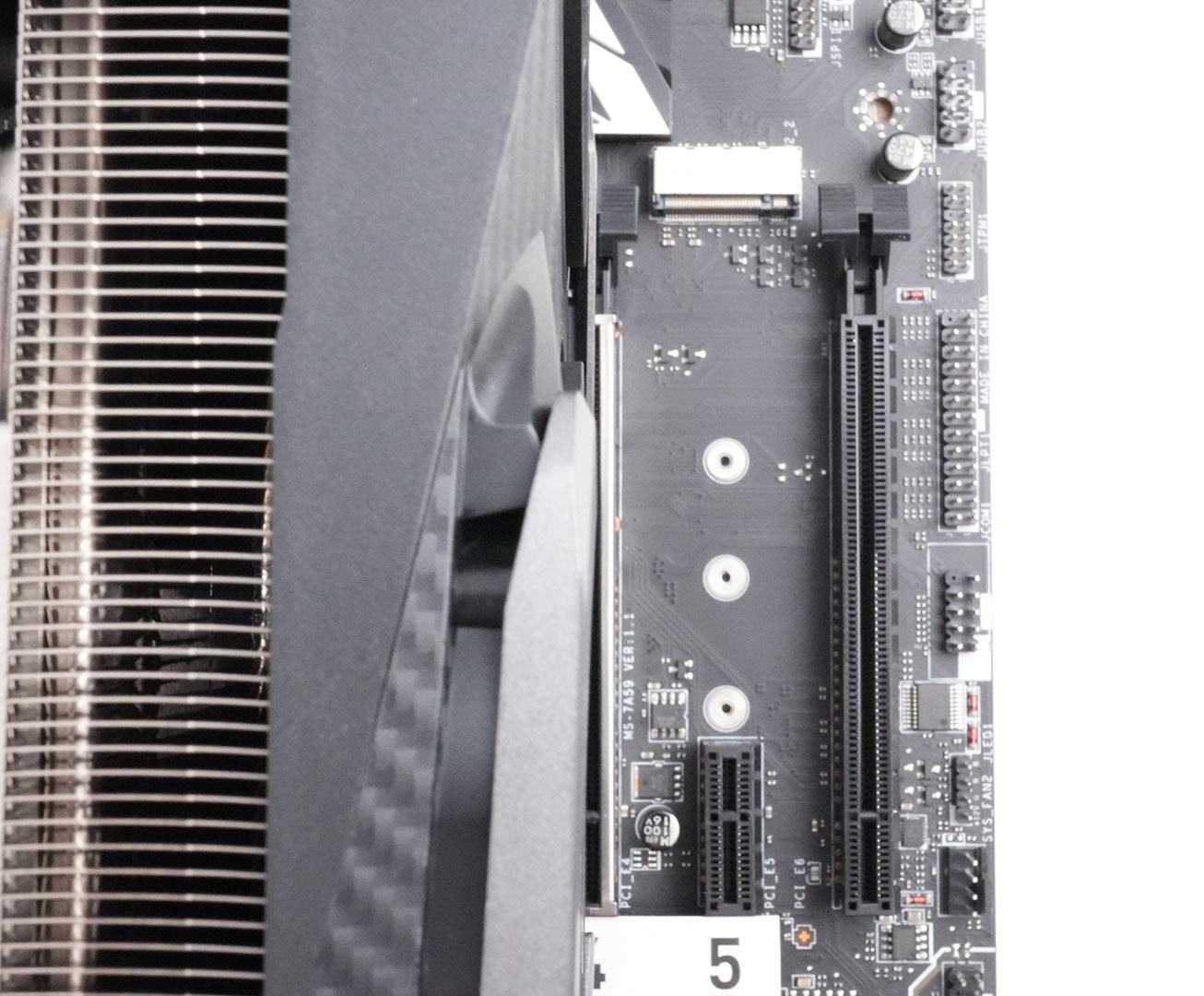
You probably saw the slot peek out on the photo above, and wondered "maybe I can still fit a card there?" No, I've tried, even a bare card won't fit into the slot. The card is maybe 2 mm too wide.
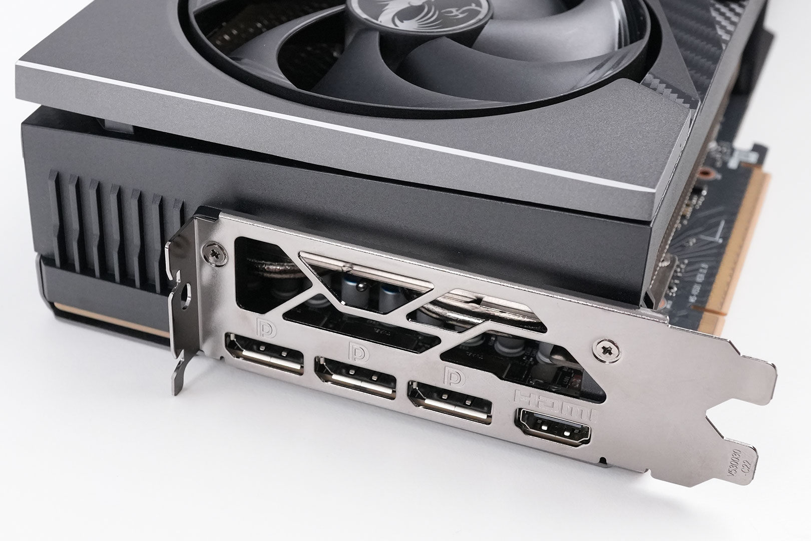
Display connectivity includes three standard DisplayPort 2.1b and a HDMI 2.1b.
Standard for all GeForce RTX 50-series Blackwell cards is a new display engine that supports three DisplayPort 2.1b outputs, each capable of UHBR20; and one HDMI 2.1a. Both interfaces support DSC (display stream compression). With DSC enabled, a single DisplayPort on this card can drive 4K 12-bit HDR at 480 Hz; or 8K 12-bit HDR at up to 165 Hz. The RTX 5070 Ti features an updated media acceleration engine with support for 4:2:2 video formats, AV1 UHQ, and MV-HEVC. There are two independent NVENC and NVDEC units.
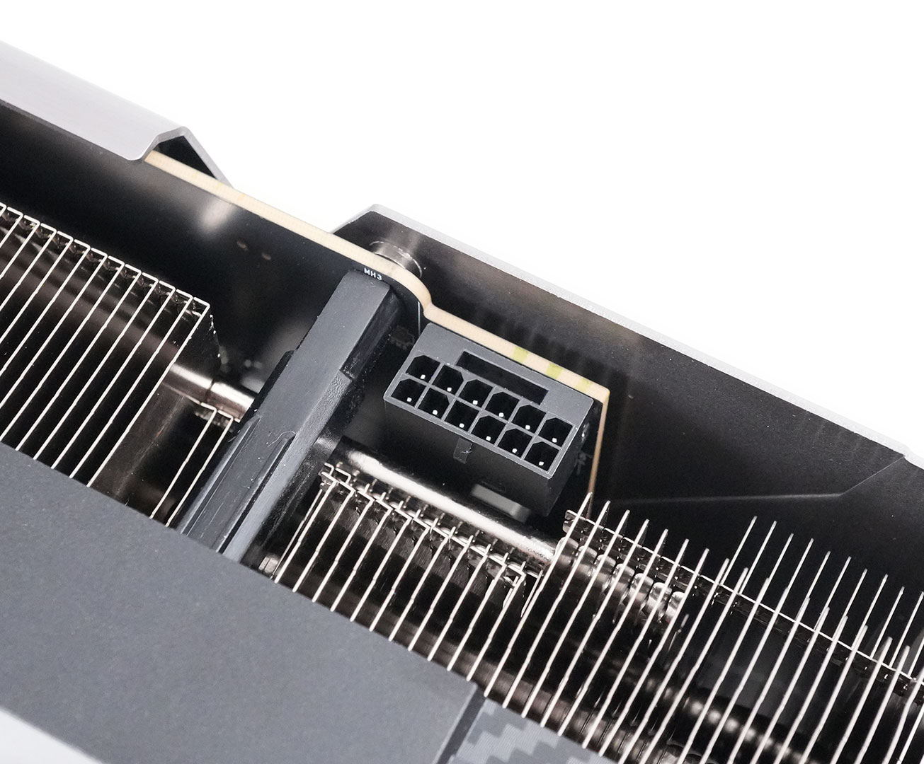
The card uses a single 16-pin connector, which allows a maximum power draw of 600 W, but the board power limit is set much lower of course.
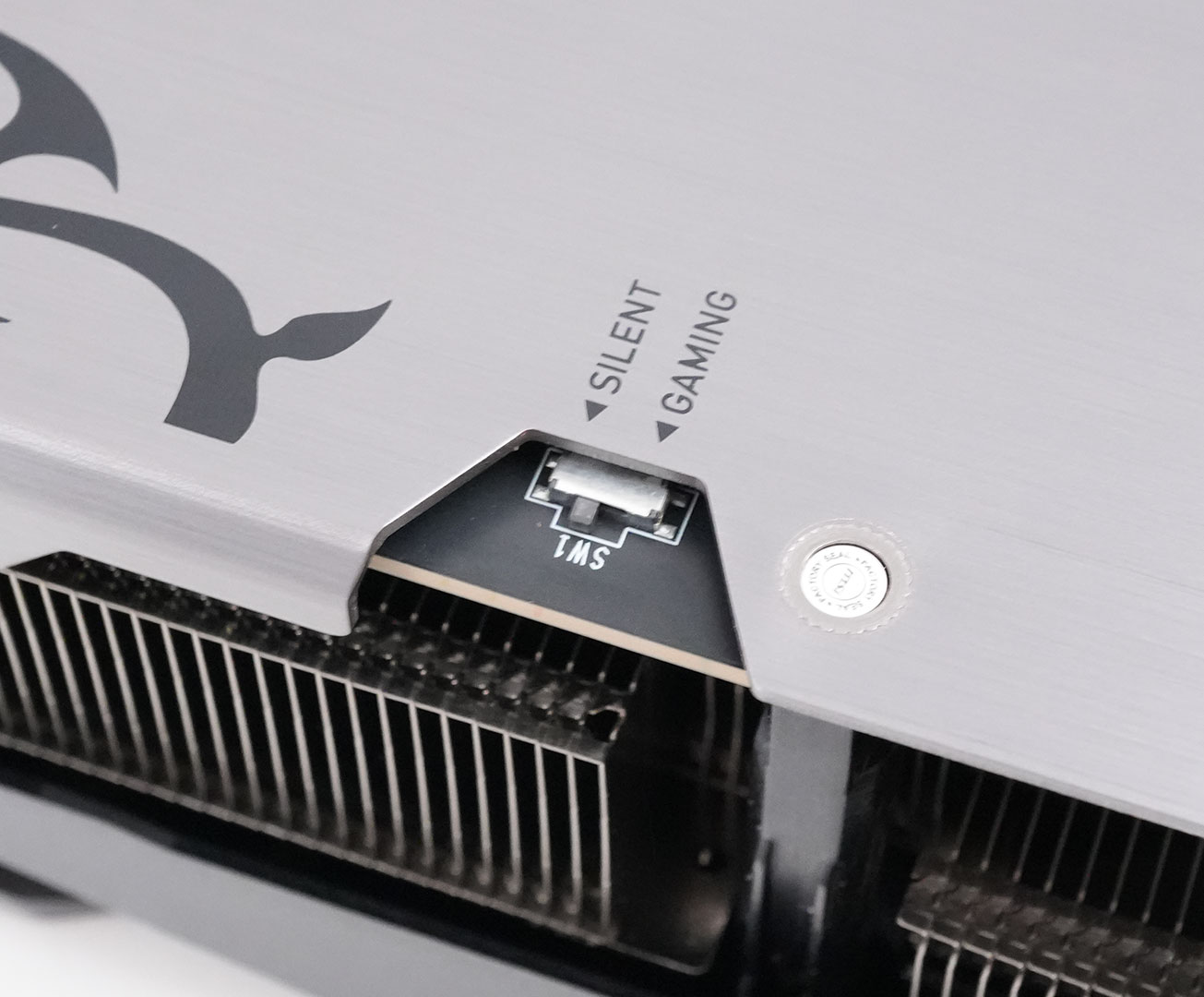
Near the IO shield is the dual BIOS switch, which lets you toggle between the default Quiet BIOS and a Performance BIOS, which runs the fans at higher speed.
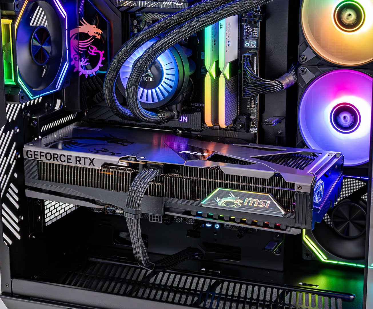
MSI has installed an RGB lighting zone on the "MSI" logo, near the fans and on the right side of the card on the second logo badge.
Our Patreon Silver Supporters can read articles in single-page format.
Mar 29th, 2025 11:21 EDT
change timezone
Latest GPU Drivers
New Forum Posts
- Upgrade from a AMD AM3+ to AM4 or AM5 chipset MB running W10? (31)
- Small chip on the tempered glass (13)
- The TPU UK Clubhouse (25998)
- Which thermal paste never pumps out? (70)
- EVGA 3070ti hotspot is too high 107.7° (5)
- Your PC ATM (35295)
- Did Nvidia purposely gimp the performance of 50xx series cards with drivers (118)
- What are you playing? (23308)
- Should you physically remove secondary NVMe drives when performing a clean Windows install? (42)
- PCI 4.0 16x slot reported as a PCI 5.0 8x with the AMD 9070 XT Reaper GPU (37)
Popular Reviews
- Sapphire Radeon RX 9070 XT Pulse Review
- Samsung 9100 Pro 2 TB Review - The Best Gen 5 SSD
- ASRock Phantom Gaming B850 Riptide Wi-Fi Review - Amazing Price/Performance
- Assassin's Creed Shadows Performance Benchmark Review - 30 GPUs Compared
- be quiet! Pure Rock Pro 3 Black Review
- Sapphire Radeon RX 9070 XT Nitro+ Review - Beating NVIDIA
- ASRock Radeon RX 9070 XT Taichi OC Review - Excellent Cooling
- Palit GeForce RTX 5070 GamingPro OC Review
- Pulsar Feinmann F01 Review
- AMD Ryzen 7 9800X3D Review - The Best Gaming Processor
Controversial News Posts
- MSI Doesn't Plan Radeon RX 9000 Series GPUs, Skips AMD RDNA 4 Generation Entirely (142)
- Microsoft Introduces Copilot for Gaming (124)
- AMD Radeon RX 9070 XT Reportedly Outperforms RTX 5080 Through Undervolting (118)
- NVIDIA Reportedly Prepares GeForce RTX 5060 and RTX 5060 Ti Unveil Tomorrow (115)
- Over 200,000 Sold Radeon RX 9070 and RX 9070 XT GPUs? AMD Says No Number was Given (100)
- NVIDIA GeForce RTX 5050, RTX 5060, and RTX 5060 Ti Specifications Leak (96)
- Retailers Anticipate Increased Radeon RX 9070 Series Prices, After Initial Shipments of "MSRP" Models (90)
- China Develops Domestic EUV Tool, ASML Monopoly in Trouble (88)