 45
45
Sapphire Radeon RX 6500 XT Pulse Review
Test Setup »High-resolution PCB Pictures
These pictures are for the convenience of volt modders and people who would like to see all the finer details on the PCB. Feel free to link back to us and use these in your articles, videos or forum posts.High-res versions are also available (front, back).
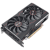
Circuit Board (PCB) Analysis
The GPU VRM is a 4+1-phase-design controlled by an OnSemi NCP81022 controller.
Vishay SiC632A DrMOS chips are used for GPU voltage.
The memory VRM is 2-phase and managed by a second OnSemi NCP81022 controller.
For memory, Vishay SiC632A DrMOS chips are used, too.
The GDDR6 memory chips are made by Samsung and carry the model number K4ZAF325BM-HC18. They are specified to run at 2250 MHz (18 Gbps GDDR6 effective).
AMD's Navi 24 graphics processor is the company's smallest RDNA 2 chip. It is fabricated using a 6 nanometer production process at TSMC Taiwan, its transistor count is 5.4 billion, and the die size is 107 mm².
Jul 5th, 2025 18:01 CDT
change timezone
Latest GPU Drivers
New Forum Posts
- EVGA XC GTX 1660 Ti 8GB ROM (11)
- How do you view TPU & the internet in general? (With poll) (79)
- What are you playing? (23893)
- Do you use Linux? (677)
- Optane performance on AMD vs Intel (58)
- Frametime spikes and stuttering after switching to AMD CPU? (521)
- Stalker 2 is looking great. (187)
- b550m aorus elite not posting with new ram (7)
- Gigabyte graphic cards - TIM gel SLIPPAGE problem (131)
- Can you guess Which game it is? (203)
Popular Reviews
- NVIDIA GeForce RTX 5050 8 GB Review
- Fractal Design Scape Review - Debut Done Right
- Crucial T710 2 TB Review - Record-Breaking Gen 5
- ASUS ROG Crosshair X870E Extreme Review
- PowerColor ALPHYN AM10 Review
- Sapphire Radeon RX 9060 XT Pulse OC 16 GB Review - An Excellent Choice
- Upcoming Hardware Launches 2025 (Updated May 2025)
- AMD Ryzen 7 9800X3D Review - The Best Gaming Processor
- Sapphire Radeon RX 9070 XT Nitro+ Review - Beating NVIDIA
- NVIDIA GeForce RTX 5060 8 GB Review
TPU on YouTube
Controversial News Posts
- Intel's Core Ultra 7 265K and 265KF CPUs Dip Below $250 (288)
- NVIDIA Grabs Market Share, AMD Loses Ground, and Intel Disappears in Latest dGPU Update (212)
- Some Intel Nova Lake CPUs Rumored to Challenge AMD's 3D V-Cache in Desktop Gaming (140)
- NVIDIA GeForce RTX 5080 SUPER Could Feature 24 GB Memory, Increased Power Limits (115)
- Microsoft Partners with AMD for Next-gen Xbox Hardware (105)
- NVIDIA Launches GeForce RTX 5050 for Desktops and Laptops, Starts at $249 (105)
- AMD Radeon RX 9070 XT Gains 9% Performance at 1440p with Latest Driver, Beats RTX 5070 Ti (102)
- Intel "Nova Lake‑S" Series: Seven SKUs, Up to 52 Cores and 150 W TDP (100)


