Mar 29th, 2025 13:17 EDT
change timezone
Latest GPU Drivers
New Forum Posts
- Dell Workstation Owners Club (3312)
- TechPowerUp Screenshot Thread (MASSIVE 56K WARNING) (4264)
- Is RX 9070 VRAM temperature regular value or hotspot? (266)
- Upgrade from a AMD AM3+ to AM4 or AM5 chipset MB running W10? (32)
- Small chip on the tempered glass (17)
- Issues with RTX4090 FE waterblock (Bitspower) (20)
- Did Nvidia purposely gimp the performance of 50xx series cards with drivers (119)
- GPU Crashing System From Hibernation (0)
- Should you physically remove secondary NVMe drives when performing a clean Windows install? (43)
- Problem with Trottlestop and HWINFO64 on MSI Raider 18 (33)
Popular Reviews
- Sapphire Radeon RX 9070 XT Pulse Review
- Samsung 9100 Pro 2 TB Review - The Best Gen 5 SSD
- ASRock Phantom Gaming B850 Riptide Wi-Fi Review - Amazing Price/Performance
- Assassin's Creed Shadows Performance Benchmark Review - 30 GPUs Compared
- Sapphire Radeon RX 9070 XT Nitro+ Review - Beating NVIDIA
- be quiet! Pure Rock Pro 3 Black Review
- ASRock Radeon RX 9070 XT Taichi OC Review - Excellent Cooling
- Palit GeForce RTX 5070 GamingPro OC Review
- Pulsar Feinmann F01 Review
- AMD Ryzen 7 9800X3D Review - The Best Gaming Processor
Controversial News Posts
- MSI Doesn't Plan Radeon RX 9000 Series GPUs, Skips AMD RDNA 4 Generation Entirely (142)
- Microsoft Introduces Copilot for Gaming (124)
- AMD Radeon RX 9070 XT Reportedly Outperforms RTX 5080 Through Undervolting (118)
- NVIDIA Reportedly Prepares GeForce RTX 5060 and RTX 5060 Ti Unveil Tomorrow (115)
- Over 200,000 Sold Radeon RX 9070 and RX 9070 XT GPUs? AMD Says No Number was Given (100)
- NVIDIA GeForce RTX 5050, RTX 5060, and RTX 5060 Ti Specifications Leak (96)
- Retailers Anticipate Increased Radeon RX 9070 Series Prices, After Initial Shipments of "MSRP" Models (90)
- China Develops Domestic EUV Tool, ASML Monopoly in Trouble (88)
 66
66
Sapphire Radeon RX 7600 XT Pulse Review
(66 Comments) »Introduction
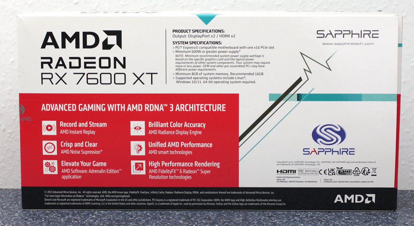
AMD today debuted the Radeon RX 7600 XT graphics card, and we have with us the Sapphire RX 7600 XT Pulse, the company's custom-design implementation. The RX 7600 XT is a purely partner-led launch—there are no reference design cards. The RX 7600 XT is recommended by AMD for maxed out AAA gaming at 1080p, as well as creator and AI workloads that can take advantage of its large 16 GB video memory. AMD is getting its partners to price the RX 7600 XT competitively to NVIDIA's GeForce RTX 4060. The Sapphire Pulse combines this with a well tuned cooling solution designed for low noise.

The Radeon RX 7600 XT is an effort by AMD to compete with the RTX 4060 within its price range, while also appealing to the creator and AI acceleration crowd. It is based on the same 6 nm Navi 33 monolithic silicon driving the RX 7600 from last year, and the RDNA 3 graphics architecture. If you recall, AMD had used up all shaders available on the Navi 33 to create the RX 7600, leaving us to wonder how it would go about creating the RX 7600 XT. One way to do it would be trying to heavily cut down the Navi 32 silicon, but that is a particularly expensive chiplet-based GPU that we doubt AMD could profitably sell under $300 or engage in a price-war with, against NVIDIA's frugal AD107 silicon driving the RTX 4060.
And yet, AMD found a way to create the RX 7600 XT. First, it doubled the memory size to 16 GB. This is across the same 128-bit GDDR6 memory interface as the RX 7600, and using double the memory chip density—an approach similar to that of the GeForce RTX 4060 Ti 16 GB. Second, the GPU engine clock speeds were dialed up. The GPU game clocks are now set at 2470 MHz compared to 2250 MHz of the RX 7600; and the maximum boost frequency set to 2760 MHz, compared to 2660 MHz of the RX 7600. For AMD GPUs, the game clock is more relevant than maximum boost, as this is the frequency the GPU holds during a typical gaming session. In that sense, this is a nearly 10% increase in engine clocks. Third, to support these clocks and ensure good boost frequency residency, AMD raised the total board power (TBP) to 190 W, compared to 165 W of the RX 7600. To support the added TBP, AMD is switching to a dual 8-pin power connector setup. As a final premium touch, AMD mandates its board partners to wire out DisplayPort 2.1, this was optional with the RX 7600, and partners could opt to provide DisplayPort 1.4a and save on some exotic SMDs needed by DP 2.1.
The RX 7600 XT, as we mentioned, is based on a maxed out Navi 33 silicon. This tiny chip physically features 32 compute units, which work out to 2,048 stream processors, 64 AI accelerators, 32 Ray accelerators, 128 TMUs, and 64 ROPs. The chip features 32 MB of Infinity Cache memory, which cushions memory transfers to the vast 16 GB of memory across its 128-bit memory bus. The card's 16 GB of GDDR6 memory ticks at 18 Gbps, producing 288 GB/s of memory bandwidth. Much like its NVIDIA competitor, the RX 7600 XT features a PCI-Express 4.0 x8 host interface, it will work on any PCIe x16 slot.
Under the hood is AMD's latest RDNA 3 graphics architecture. There are several architectural improvements, including the new generation compute unit, which in addition to a 17% IPC gain over the RDNA 2 CU, supports new math formats, and dual instruction issue rate. Each CU features two AI accelerators, a new component AMD introduced with RDNA 3, which prepares matrix math workloads for processing by the SIMD units of the CU. The second generation Ray accelerator incorporates several design improvements over RDNA 2, offering a 50% generational increase in ray intersection performance. RDNA 3 also introduces MDIA (multi draw indirect accelerator), a hardware component that provides a 2.3x speedup for specific DirectX 12 draw commands, and reducing CPU API and driver overhead. Lastly, the Navi 33 supports AMD Radiance Display Engine (RDE), which supports the latest DisplayPort 2.1 UHBR13.5, and USB-C with DisplayPort 2.1 passthrough, for supporting several new display types.
AMD is pricing the Radeon RX 7600 XT at a starting price of $330, or a $60 (22%) premium over the RX 7600, which is also Sapphire's asking price for this card. The Sapphire RX 7600 XT Pulse comes with a dual-slot, dual-fan cooling solution, using an aluminium fin-stack heatsink, and a pair of fans that are easy to detach without disturbing the heatsink underneath, so you can keep your graphics card clean. The card features a unique display output configuration of two DisplayPort 2.1, and two HDMI 2.1a connectors. In this review, we find out what the RX 7600 XT brings to the table, particularly over the RX 7600, and whether the RTX 4060 stares at a challenger.
Short 10-Minute Video Comparing 10x RTX 4070 Ti Super
Our goal with the videos is to create short summaries, not go into all the details and test results, which can be found in our written reviews.
| Price | Cores | ROPs | Core Clock | Boost Clock | Memory Clock | GPU | Transistors | Memory | |
|---|---|---|---|---|---|---|---|---|---|
| RTX 3050 | $230 | 2560 | 32 | 1552 MHz | 1777 MHz | 1750 MHz | GA106 | 12000M | 8 GB, GDDR6, 128-bit |
| Arc A750 | $200 | 3584 | 112 | 2050 MHz | N/A | 2000 MHz | ACM-G10 | 21700M | 8 GB, GDDR6, 256-bit |
| RX 6600 | $170 | 1792 | 64 | 2044 MHz | 2491 MHz | 1750 MHz | Navi 23 | 11060M | 8 GB, GDDR6, 128-bit |
| RX 6600 XT | $200 | 2048 | 64 | 2359 MHz | 2589 MHz | 2000 MHz | Navi 23 | 11060M | 8 GB, GDDR6, 128-bit |
| RTX 3060 | $240 | 3584 | 48 | 1320 MHz | 1777 MHz | 1875 MHz | GA106 | 12000M | 12 GB, GDDR6, 192-bit |
| RX 7600 | $270 | 2048 | 64 | 2250 MHz | 2625 MHz | 2250 MHz | Navi 33 | 13300M | 8 GB, GDDR6, 128-bit |
| RX 7600 XT | $330 | 2048 | 64 | 2470 MHz | 2755 MHz | 2250 MHz | Navi 33 | 13300M | 16 GB, GDDR6, 128-bit |
| Sapphire RX 7600 XT Pulse | $330 | 2048 | 64 | 2539 MHz | 2810 MHz | 2250 MHz | Navi 33 | 13300M | 16 GB, GDDR6, 128-bit |
| RTX 4060 | $300 | 3072 | 48 | 1830 MHz | 2460 MHz | 2125 MHz | AD107 | 18900M | 8 GB, GDDR6, 128-bit |
| Arc A770 | $300 | 4096 | 128 | 2100 MHz | N/A | 2187 MHz | ACM-G10 | 21700M | 16 GB, GDDR6, 256-bit |
| RTX 3060 Ti | $250 | 4864 | 80 | 1410 MHz | 1665 MHz | 1750 MHz | GA104 | 17400M | 8 GB, GDDR6, 256-bit |
| RTX 4060 Ti | $390 | 4352 | 48 | 2310 MHz | 2535 MHz | 2250 MHz | AD106 | 22900M | 8 GB, GDDR6, 128-bit |
| RX 6700 XT | $300 | 2560 | 64 | 2424 MHz | 2581 MHz | 2000 MHz | Navi 22 | 17200M | 12 GB, GDDR6, 192-bit |
| RTX 3070 | $310 | 5888 | 96 | 1500 MHz | 1725 MHz | 1750 MHz | GA104 | 17400M | 8 GB, GDDR6, 256-bit |
| RTX 3070 Ti | $350 | 6144 | 96 | 1575 MHz | 1770 MHz | 1188 MHz | GA104 | 17400M | 8 GB, GDDR6X, 256-bit |
| RX 7700 XT | $430 | 3456 | 96 | 2171 MHz | 2544 MHz | 2250 MHz | Navi 32 | 26500M | 12 GB, GDDR6, 192-bit |
AMD RDNA 3 Graphics Architecture

The new Radeon RX 7600 XT is based on the latest RDNA 3 graphics architecture by AMD, which aims to take advantage of newer architecture-level advancements, newer components such as the AI accelerators, 2nd gen Ray accelerator, and MDIA, to provide generational speedups. For the higher end models in the Radeon RX 7000 series, starting the RX 7700 XT and upward, AMD is using 5 nm EUV foundry process, at least where it matters—the shader engines. The RX 7600 series, on the other hand, is based on the monolithic Navi 33 silicon that's based on the slightly older 6 nm DUV foundry node, which AMD thinks has sufficient electrical and thermal characteristics for a mid-range GPU that can be produced in a cost-efficient manner, with room for price-cuts. The silicon comes with a die-area of 204 mm², and a transistor count of 13.3 billion.
The 6 nm Navi 33 silicon, as we mentioned, physically features a maximum of 32 CU (compute units). This works out to 2,048 stream processors. Each CU contains two AI accelerators, and a 2nd gen Ray accelerator, which works out to 64 AI accelerators, and 32 Ray accelerators in all for the RX 7600 XT. Other critical specs include 128 TMUs, and 64 ROPs. The chip's 128-bit GDDR6 memory interface drives 16 GB of memory on the RX 7600 XT, which ticks at 18 Gbps, giving it 288 GB/s of memory bandwidth on tap. This is cushioned by a 32 MB on-die Infinity Cache. AMD hasn't released an architectural diagram for the Navi 33, yet.
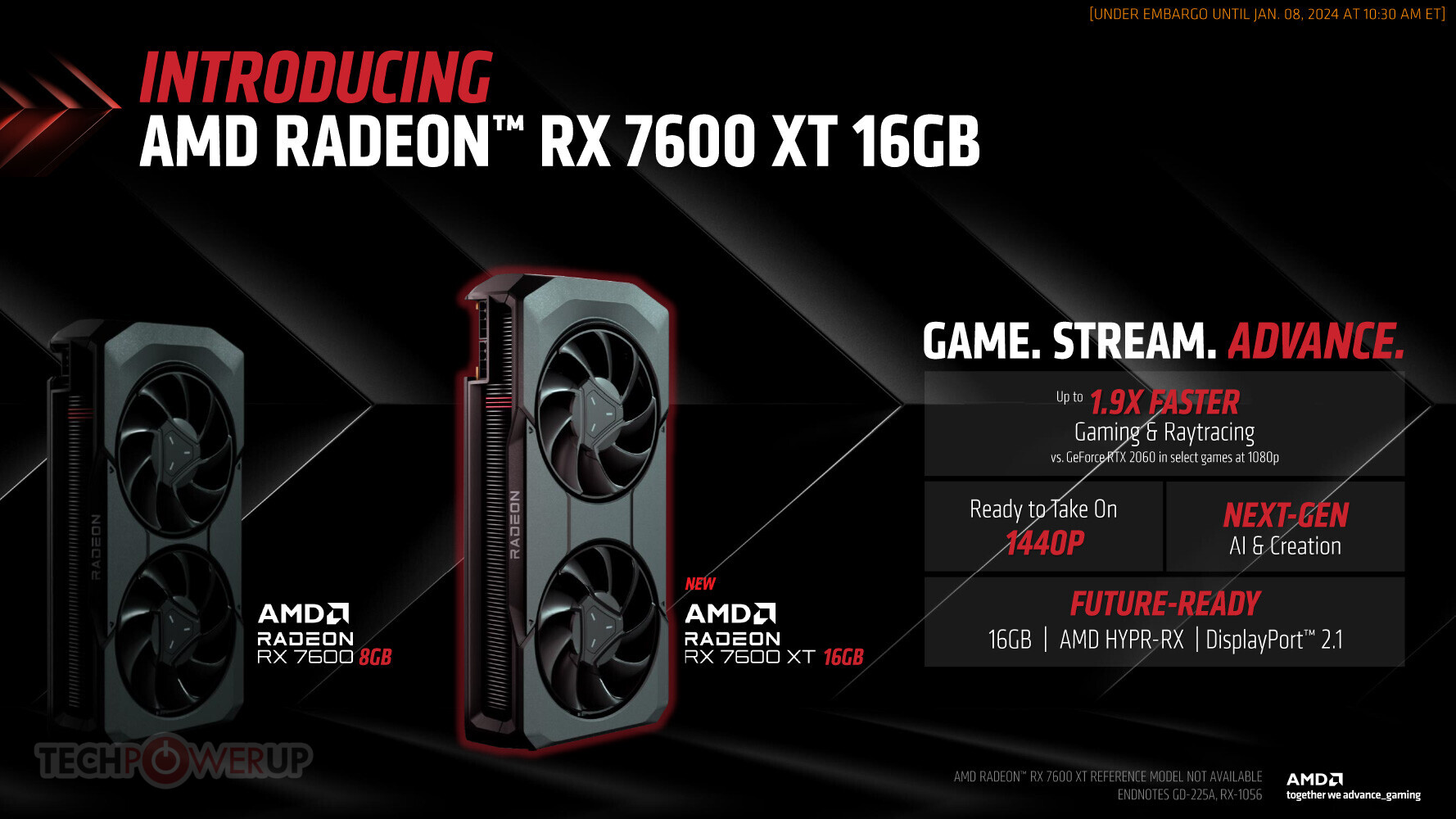
Much of the architectural innovation is this generation is with the RDNA 3 Dual-Compute Unit (or Compute Unit pair). The "Navi 33" GPU physically features 32 compute units spread across two Shader Engines. AMD claims that at the same engine clocks, the RDNA 3 CU offers a 17.4% IPC increase over the RDNA 2 CU.
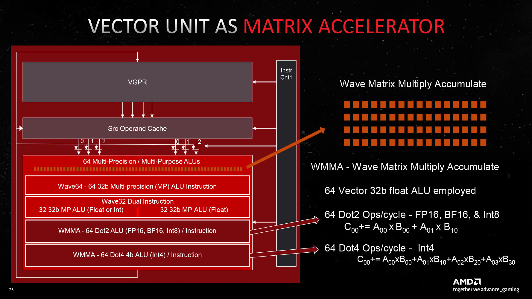
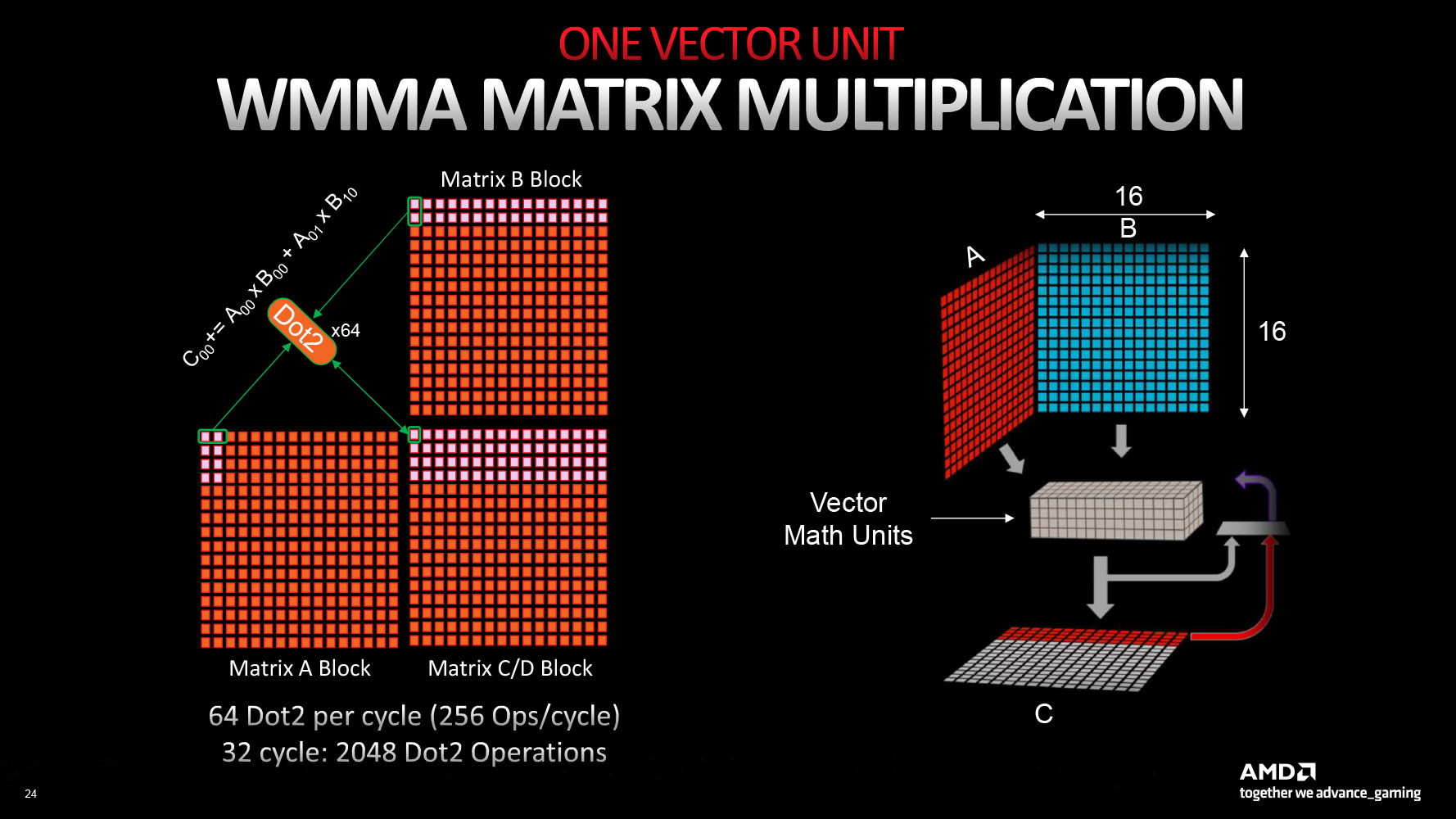
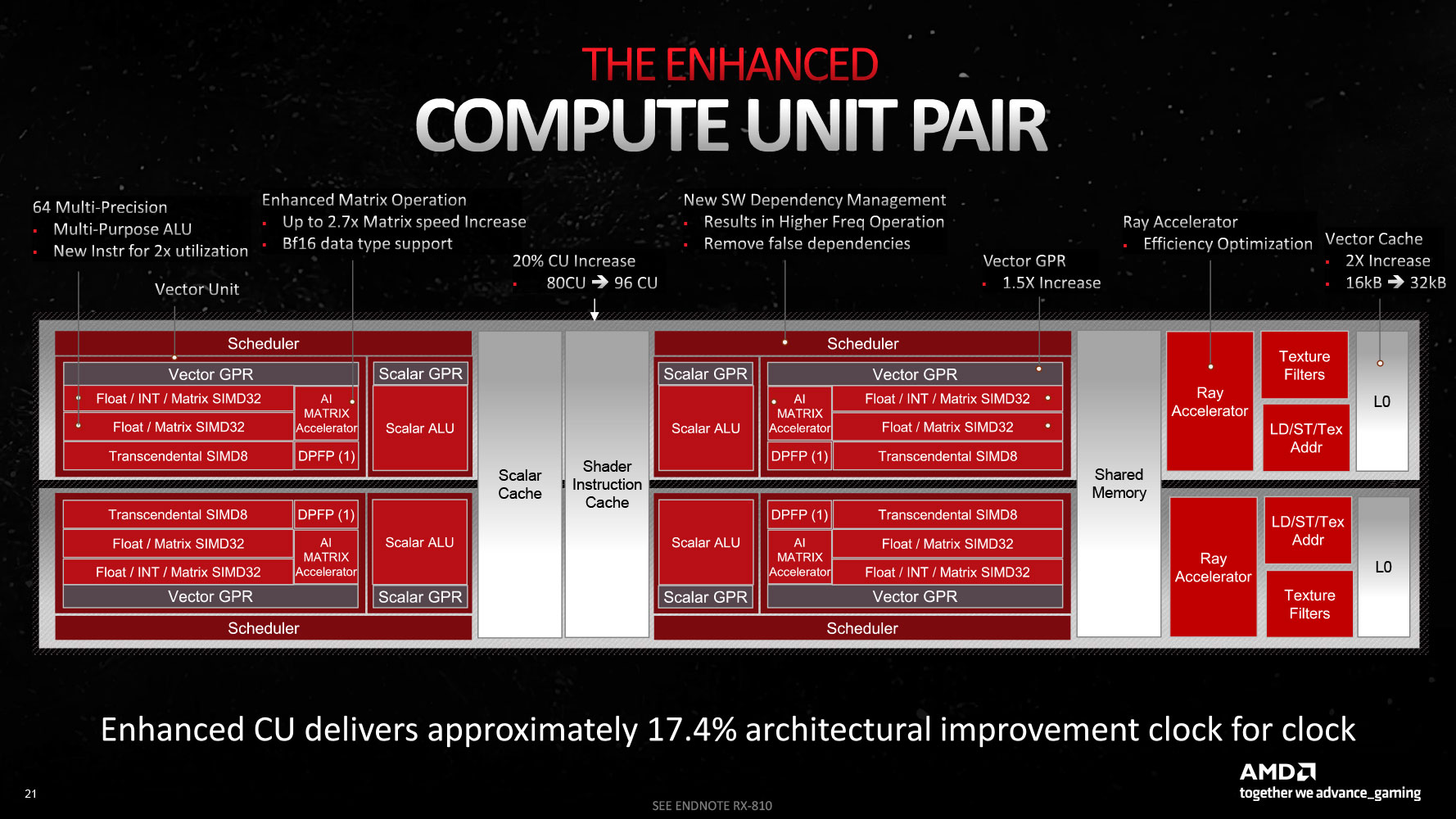
The new RDNA 3 CU introduces multi-precision capability for the 64 stream processors per CU: operating either as 1x SIMD64 or 2x SIMD32 units. The Vector Unit that houses these SIMD units can either function as a SIMD execution mechanism, or as a Matrix execution unit, thanks to the new AI Matrix Accelerator, which provides a 2.7x matrix multiplication performance uplift versus conventional SIMD execution. Also added are support for the Bfloat16 instruction-set, and SIMD8 execution. The GPU hence enjoys AI hardware-acceleration that can be leveraged in future feature-additions relevant to gamers, such as FSR 3.0. Game developers will also look for ways to exploit accelerated AI, now that all three brands feature it (NVIDIA Tensor cores and Intel XMX cores).

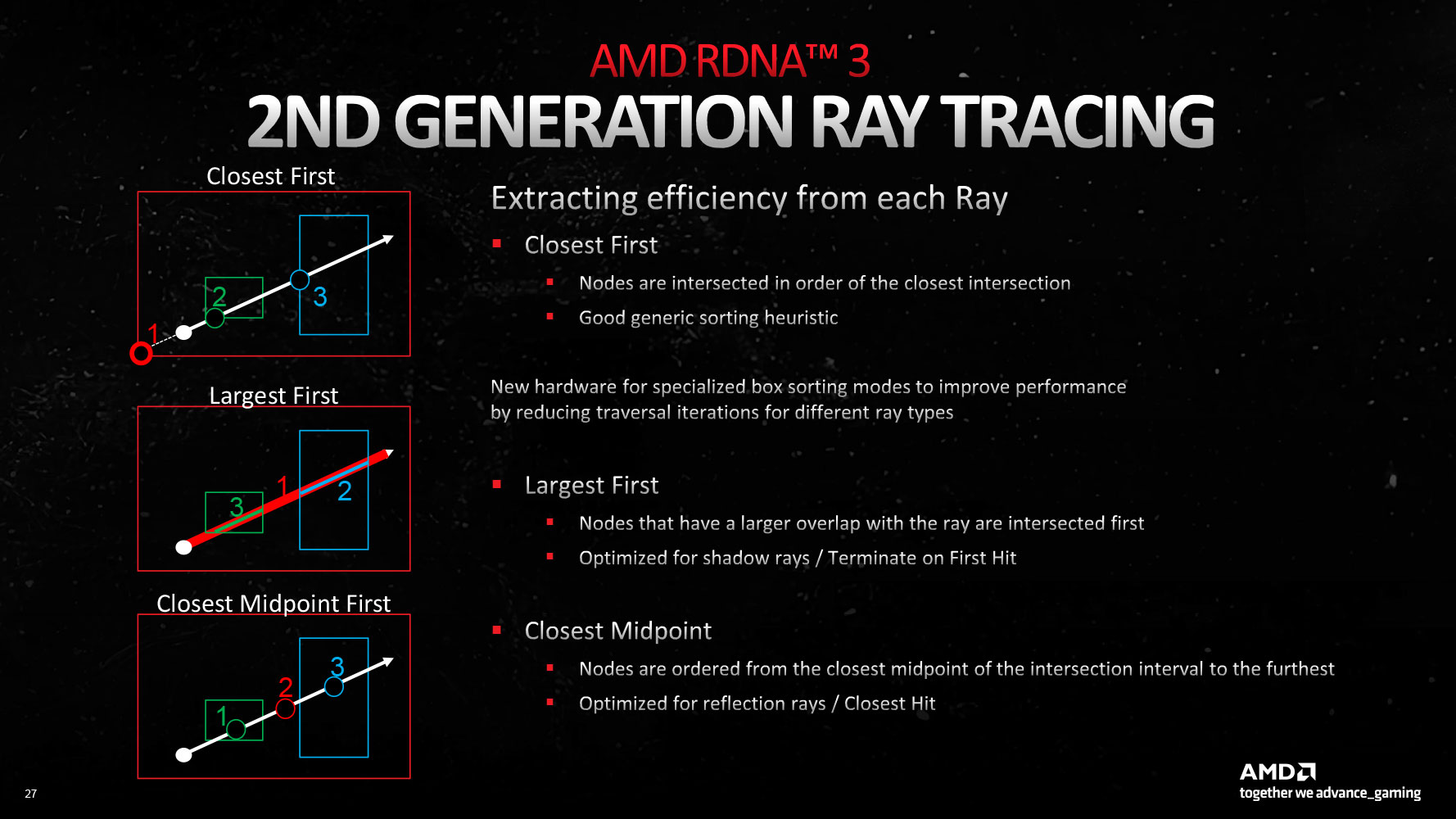
AMD's first-generation Ray Accelerator, introduced with the RDNA 2 architecture, was the result of a hasty effort to catch up to NVIDIA with a DirectX 12 Ultimate GPU, where they developed a fixed-function hardware to calculate ray intersections, and offloaded a large chunk of RT processing to the generationally-doubled SIMD resources. With RDNA 3, they've refined the Ray Accelerator to achieve an 80% ray tracing performance uplift over the previous generation, when you add up the Ray Accelerator count, their higher engine clocks, and other hardware-level optimizations, such as early sub-tree culling, specialized box sorting modes, and reduced traversal iterations.
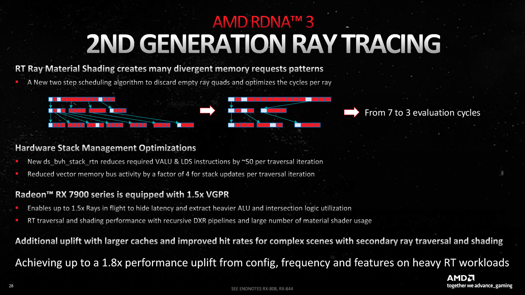
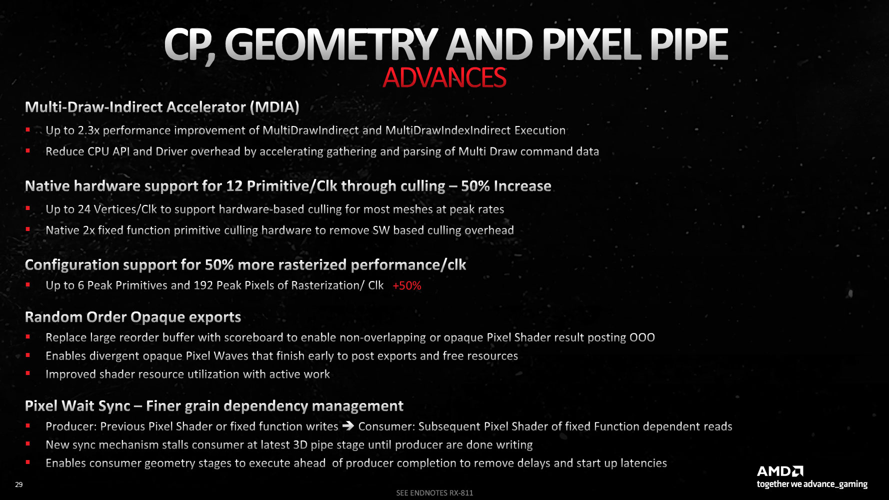
There is a 50% ray intersection capacity improvement for RDNA 3 thanks to these optimizations, and cycles-per-ray reduction. Besides these, AMD has also made several improvements to the geometry- and pixel-pipes, with the introduction of the new multi-draw indirect accelerator (MDIA), which reduces CPU API and driver-level overheads by gathering and parsing of multi-draw command data. At the hardware-level 12 primitives per clock is now supported compared to 8 per clock on RDNA 2, thanks to culling. The core-configuration overall enables 50% more rasterized performance per clock.
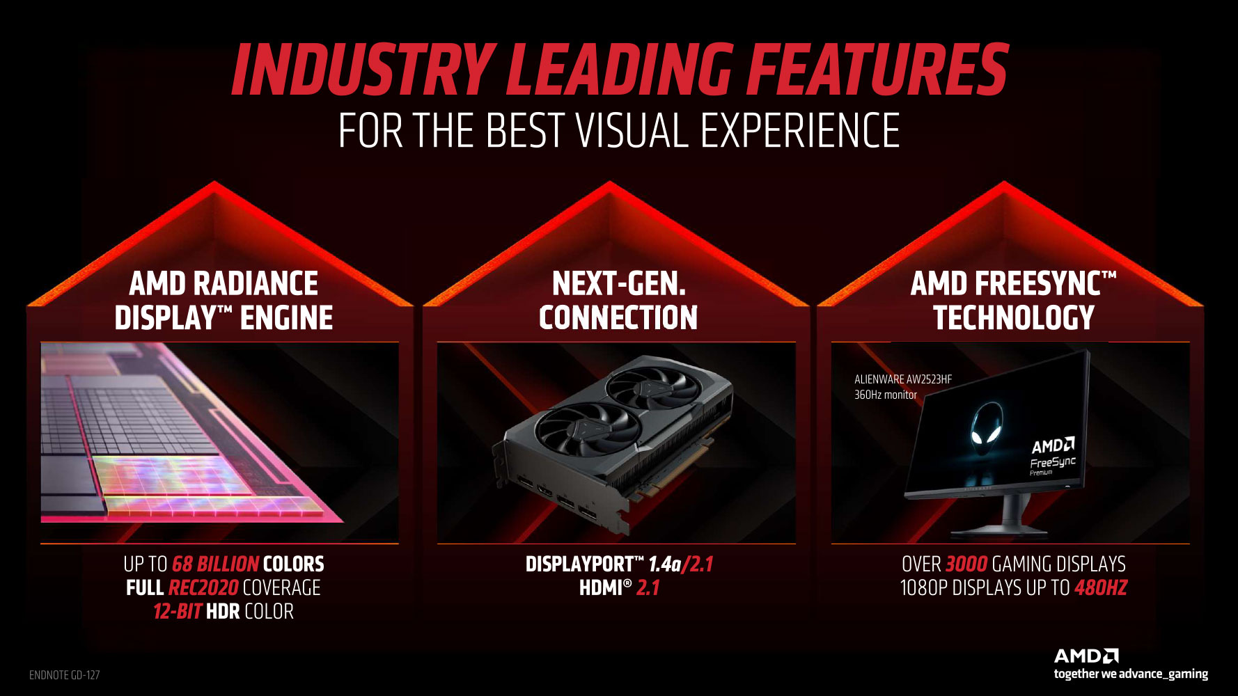
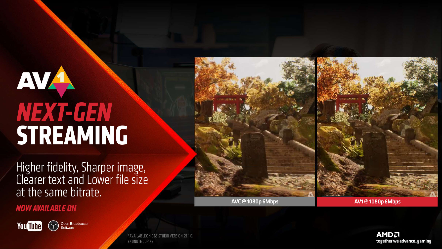
AMD has significantly improved the Display Engine of "Navi 33" over the previous-generation in terms of connectivity. The new Radiance Display Engine comes with native support for DisplayPort 2.1, which enables 8K output at up to 165 Hz refresh-rate, or 4K at up to 480 Hz, with a single cable. AMD has refined its FSR 2 algorithm to support 8K (i.e. render at a lower resolution with FSR-enhanced upscaling), to make it possible to enjoy the latest AAA titles at playable frame-rates on 8K displays. The RX 7600 XT gets two full-size DP 2.1 connectors, besides an HDMI 2.1b, and a USB-C with DP 2.1 passthrough. Unlike with the RX 7600, board partners cannot opt to have DisplayPort 1.4a for RX 7600 XT cards. The "Navi 33" silicon receives full hardware-accelerated AV1 encode and decode capabilities. With this generation, AMD is also introducing SmartAccess Video, a feature that lets the AMD driver leverage the hardware encoders of the RDNA 2 iGPU of Ryzen 7000 desktop processors, for additional encoding performance.
FidelityFX SuperResolution 3 Fluid Motion Frames (FSR 3 and FMF)
As part of the Radeon RX 7800 XT and RX 7700 XT announcements, AMD finally announced the much awaited FidelityFX Super Resolution 3 and Fluid Motion Frames. FSR 3 is being announced as a technological rival to NVIDIA DLSS 3 Frame Generation. The premise with both technologies is the same—to effectively double frame-rates by generating alternate frames without running them through the entire graphics rendering pipeline, it's just that the two technologies differ in their approach to this goal.
FSR 3 builds on FSR 2 with its updated super resolution upscaler promising generational quality improvements at a every given rendering resolution. Fluid Motion Frames (FMF) isn't the entirety of the FSR 3 feature-set, but is its most important feature-addition. FMF is a frame interpolation technology much like the one consumer televisions come with. Alternate frames are generated as an approximate of two frames. Where FMF differs from DLSS 3 Frame Generation is that while NVIDIA uses a hardware component called optical flow accelerator and the GPU's AI acceleration to generate an intermediate frame without involving the graphics rendering pipeline, FMF uses a certain amount of the graphics rendering pipeline. At a hardware level, FMF uses the main SIMD machinery of the GPU, leveraging asynchronous compute. As with DLSS 3 FG, FSR 3 FMF comes with added latency. NVIDIA counteracts this with Reflex, while AMD uses Radeon AntiLag+. Both technologies try to keep the frame queue short to reduce whole system latencies.
One major advantage FSR 3 FMF enjoys over DLSS 3 FG is that it works on any modern DirectX 12 GPU that supports async compute, since it doesn't require a specific hardware component the way DLSS 3 FG requires the Optical Flow Accelerator on NVIDIA "Ada" GPUs. The only limiting factor here is the performance. To be more specific, AMD says that all Radeon GPUs from RX 5700 series onward; and all GeForce GPUs from RTX 20-series onward, should support FSR 3 FMF. Also, FSR 3 FMF is as easy to integrate with games as FSR 2 is. The first games implementing FSR 3 FMF should arrive in Fall 2023. AMD is also working to extend FMF to Radeon Super Resolution, the driver-level technology that enables performance upscaling to even games that don't support FSR.
HYPR-RX
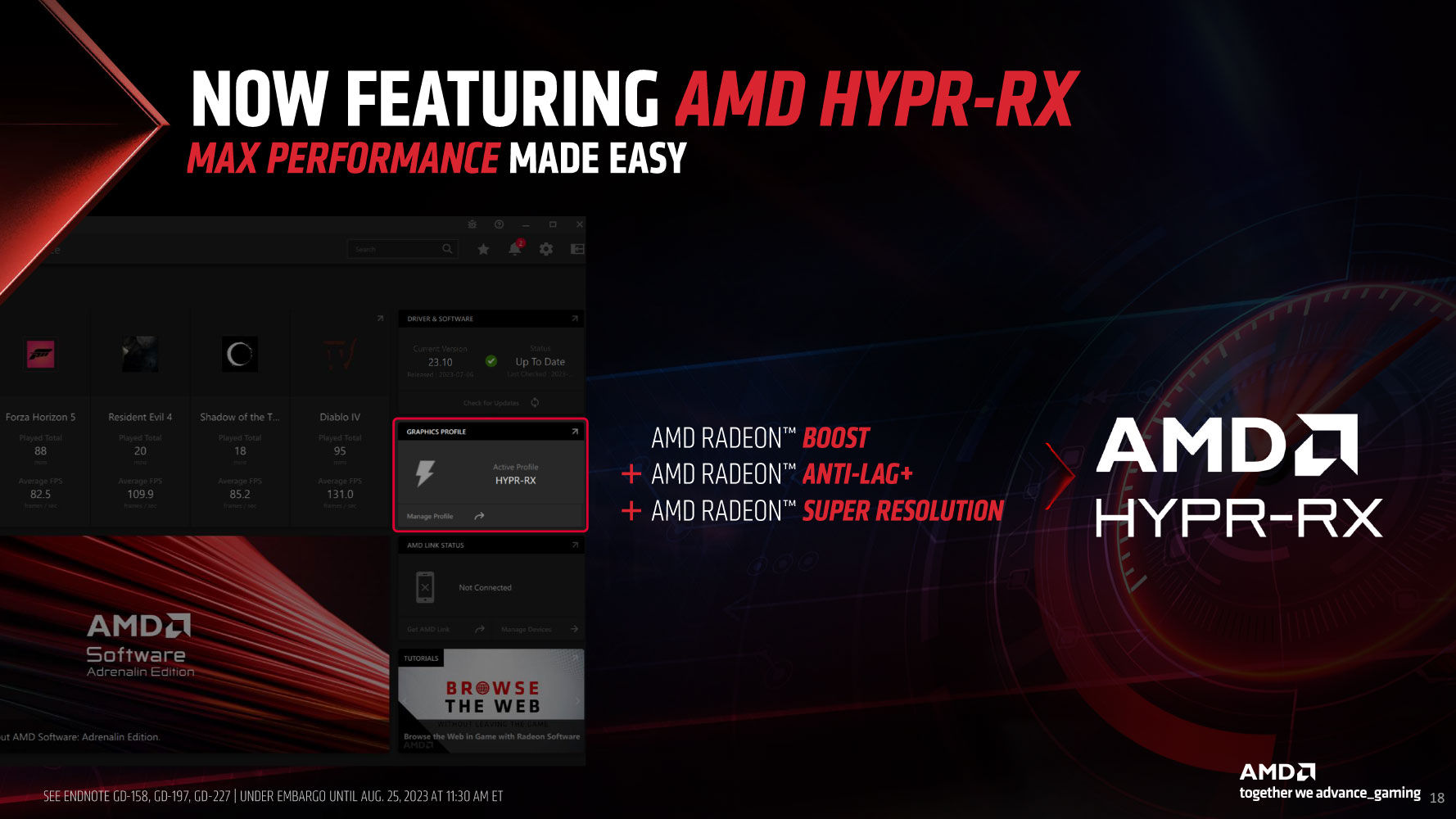
HYPR-RX is an interesting new feature in the AMD Software (control center) application. It is a one-click performance boosting technology that works with any DirectX 11 or DirectX 12 game. The software is a cocktail of Radeon Boost, Radeon AntiLag+, and Radeon Super Resolution, and applies the three features on any running game as needed, automatically. Radeon Boost improves performance by dynamically reducing the render resolution of a game when there's too much motion on the screen (and hence not enough detail needed). Radeon Super Resolution improves frame-rates as it applies FSR on the output of a game rendered at a lower resolution (including the frames lowered in resolution by Radeon Boost. AntiLag+ counteracts the latency added by these two, by shortening the frame queue. AFMF is part of the HYPR-RX feature-set, which can be activated with a single click.
Packaging

The Card
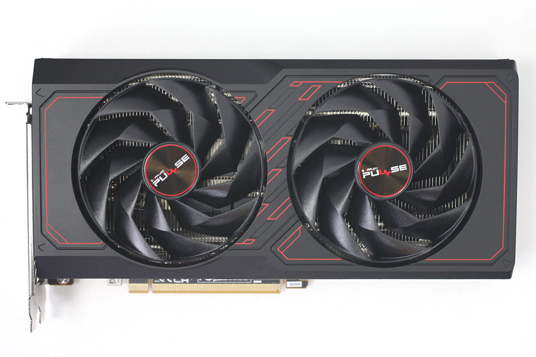

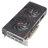
The Sapphire Radeon RX 7600 Pulse comes with a fresh cooling solution design that retains the minimalist red-on-black color scheme of the series. There's no fancy RGB lighting to be had, whatever visual uplift is from the design itself. The cooler shroud is made of plastic, but the backplate is metal.


Dimensions of the card are 25.0 x 13.0 cm, and it weighs 792 g.


Installation requires two slots in your system. We measured the card's width to be 44 mm.

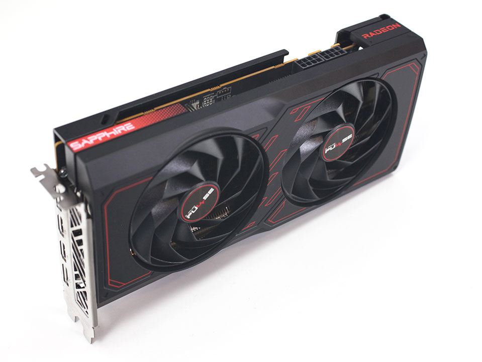
Display connectivity includes two standard DisplayPort 2.1 ports (RDNA 2 had 1.4a) and two HDMI 2.1a (same as RDNA 2).
AMD has upgraded their encode/decode setup. It now comes with two independent hardware units that can encode and decode two streams of video in parallel, or one stream at double the FPS rate. There's support for VP9, H.264, H.265 and AV1 decode, and encoding is supported for H.264, H.265 and AV1.

All Radeon RX 7600 XT cards use two 8-pin power connectors.
Our Patreon Silver Supporters can read articles in single-page format.
Mar 29th, 2025 13:17 EDT
change timezone
Latest GPU Drivers
New Forum Posts
- Dell Workstation Owners Club (3312)
- TechPowerUp Screenshot Thread (MASSIVE 56K WARNING) (4264)
- Is RX 9070 VRAM temperature regular value or hotspot? (266)
- Upgrade from a AMD AM3+ to AM4 or AM5 chipset MB running W10? (32)
- Small chip on the tempered glass (17)
- Issues with RTX4090 FE waterblock (Bitspower) (20)
- Did Nvidia purposely gimp the performance of 50xx series cards with drivers (119)
- GPU Crashing System From Hibernation (0)
- Should you physically remove secondary NVMe drives when performing a clean Windows install? (43)
- Problem with Trottlestop and HWINFO64 on MSI Raider 18 (33)
Popular Reviews
- Sapphire Radeon RX 9070 XT Pulse Review
- Samsung 9100 Pro 2 TB Review - The Best Gen 5 SSD
- ASRock Phantom Gaming B850 Riptide Wi-Fi Review - Amazing Price/Performance
- Assassin's Creed Shadows Performance Benchmark Review - 30 GPUs Compared
- Sapphire Radeon RX 9070 XT Nitro+ Review - Beating NVIDIA
- be quiet! Pure Rock Pro 3 Black Review
- ASRock Radeon RX 9070 XT Taichi OC Review - Excellent Cooling
- Palit GeForce RTX 5070 GamingPro OC Review
- Pulsar Feinmann F01 Review
- AMD Ryzen 7 9800X3D Review - The Best Gaming Processor
Controversial News Posts
- MSI Doesn't Plan Radeon RX 9000 Series GPUs, Skips AMD RDNA 4 Generation Entirely (142)
- Microsoft Introduces Copilot for Gaming (124)
- AMD Radeon RX 9070 XT Reportedly Outperforms RTX 5080 Through Undervolting (118)
- NVIDIA Reportedly Prepares GeForce RTX 5060 and RTX 5060 Ti Unveil Tomorrow (115)
- Over 200,000 Sold Radeon RX 9070 and RX 9070 XT GPUs? AMD Says No Number was Given (100)
- NVIDIA GeForce RTX 5050, RTX 5060, and RTX 5060 Ti Specifications Leak (96)
- Retailers Anticipate Increased Radeon RX 9070 Series Prices, After Initial Shipments of "MSRP" Models (90)
- China Develops Domestic EUV Tool, ASML Monopoly in Trouble (88)