 380
380
Sapphire Radeon RX 9070 XT Nitro+ Review - Beating NVIDIA
FSR 4 & AMD Software »AMD RDNA 4 Architecture
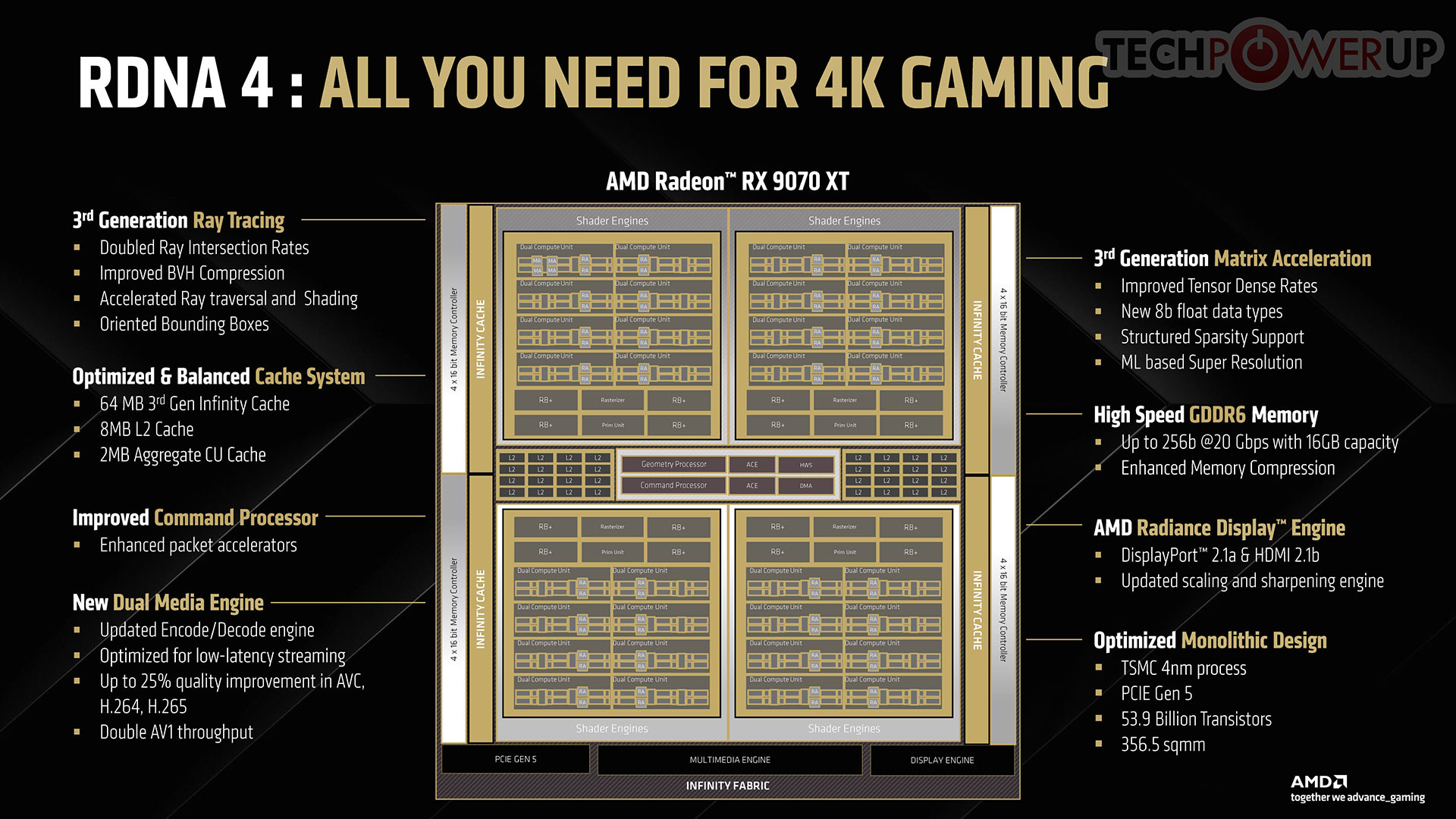

The new Radeon RX 9070 XT and RX 9070 are powered by the 4 nm Navi 48 silicon. Unlike the Navi 31 and Navi 32 before it, this is a traditional monolithic die built entirely on the TSMC N4P (4 nm EUV) process node. It has an area of 356.5 mm², but with an impressive transistor count of 53.9 billion. To put this number into context, the previous "big Navi" GPU, the Navi 31 powering the RX 7900 XTX, has 57.8 billion transistors (just 8% more), despite having 96 CU, a larger Infinity Cache, and a wider 384-bit memory bus. Navi 31 has a die area of 529 mm² (304 mm² for the 5 nm GCD, with the rest being 6 nm MCDs), so you can see the kind of strides AMD made with die-area. At the top-level, the Navi 48 features a PCI-Express 5.0 x16 host interface and a 256-bit wide GDDR6 memory bus. With 20 Gbps GDDR6 memory chips, the RX 9070 XT gets 640 GB/s of memory bandwidth. This is made up for with a faster 64 MB Infinity Cache, and a critical improvement AMD made to its memory management system, called Out-of-Order Memory Queuing.
The Navi 48 silicon physically has 64 CU spread across 4 shader engines. With each CU containing 64 stream processors, the chip has a total of 4,096 stream processors. All 64 CU are enabled on the RX 9070 XT, while the RX 9070 has 56 out of 64 of them enabled. The maxed-out Navi 48 contains 4,096 stream processors, 128 AI accelerators, 64 RT accelerators, 256 TMUs, and 128 ROPs. The chip also features 64 MB of 3rd Gen Infinity Cache, and a 256-bit wide GDDR6 memory interface, driving 16 GB of 20 Gbps memory on both the RX 9070 XT and RX 9070. With 56 CU enabled on the RX 9070, it has 3,584 stream processors, 112 AI accelerators, 56 RT accelerators, 224 TMUs, and an untouched ROP count of 128, besides the exact same memory configuration as the RX 9070 XT.
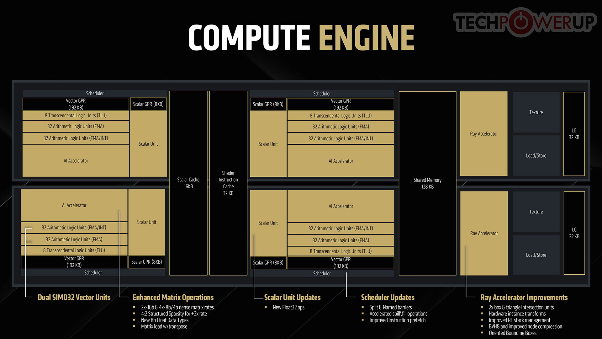
At the heart of the RDNA 4 graphics architecture is the new dual compute unit, with a vastly improved memory sub-system, improvements made to the scalar units, a new technology called dynamic register allocation, and improvements to CU efficiency and engine clocks. Each CU has two scheduler blocks, driving a 192 KB general purpose register (GPR), an 8 KB scalar GPR, 32 FMA ALUs, and 32 FMA+INT ALUs. There are also 8 transcendental logic units. RDNA 4 introduces the concept of dual SIMD32 vector units, for even more parallelism. The Scalar Unit comes with support for newer Float32 ops. Schedulers are updated with accelerated spill/fill operations. Instruction prefetching is improved. The new generation AI Accelerator comes with two 16-bit and four 8-bit/4-bit dense matrix compute rates, support for 4:2 structured sparsity for doubling throughput, and matrix loads with transpose. AMD has incorporated many technologies from its CDNA 3 Radeon Instinct AI ML accelerators on the AI Accelerators of RDNA 4, including enhanced and power-optimized WMMA, improvements to the ops per CU, support for FP8, E4M3 and E5M2 formats, and 4:2 structured sparsity.
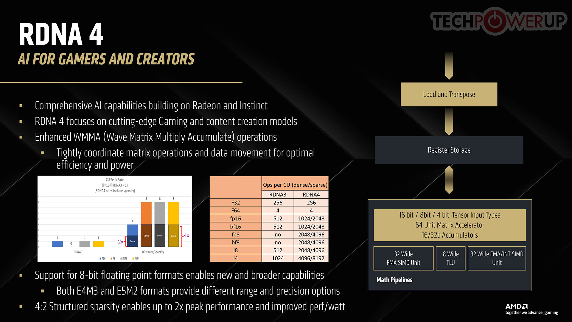
The new generation AI Accelerator comes with two 16-bit and four 8-bit/4-bit dense matrix compute rates, support for 4:2 structured sparsity for doubling throughput, and matrix loads with transpose. AMD has incorporated many technologies from its CDNA 3 Radeon Instinct AI ML accelerators on the AI Accelerators of RDNA 4, including enhanced and power-optimized WMMA, improvements to the ops per CU, support for FP8, E4M3 and E5M2 formats, and 4:2 structured sparsity.
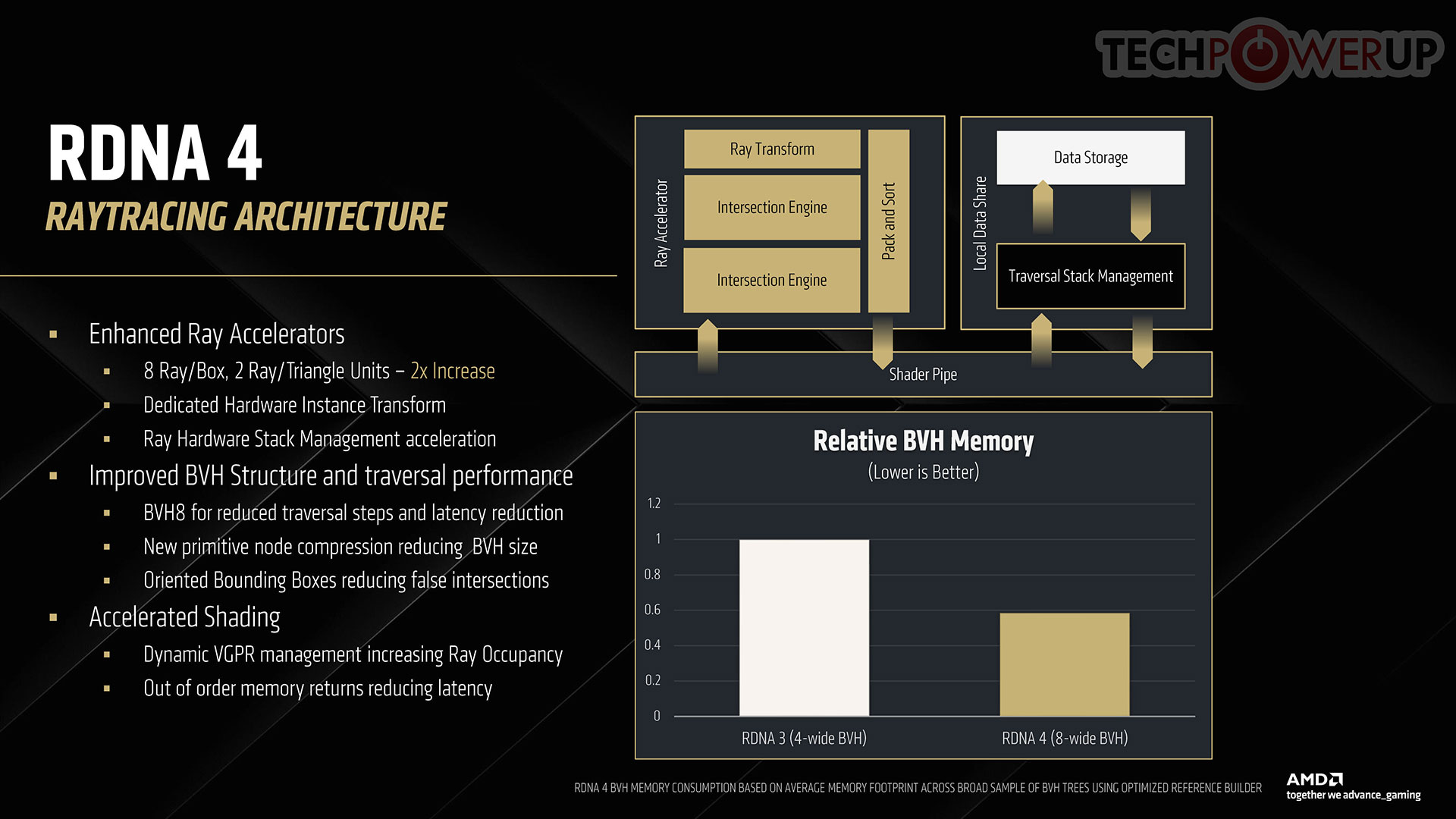
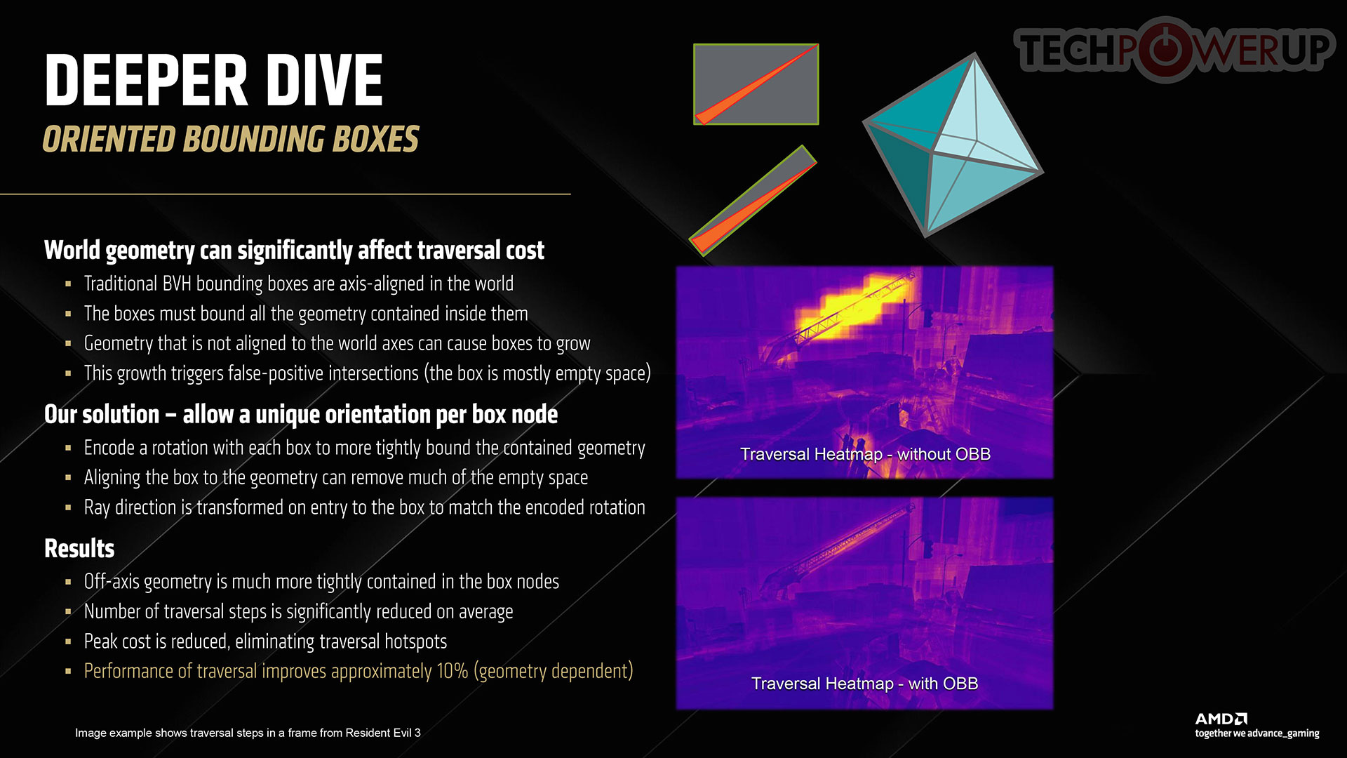
The new generation Ray Accelerator comes with double the box and triangle intersection resources as RDNA 3 RT accelerator, support for hardware instance transforms, improvements to the RT stack management, BVH8 node compression, and a revolutionary feature called oriented bounding boxes. To contain the number of rays really needed to be tested against an object, modern ray tracing technologies use something called a bounding box, which defines a region in which a geometry has to be tested against rays. Most of the time, the geometry is of a vastly different shape and smaller than the shape of a bounding box, which introduces false intersections, and wastes ray testing resources. AMD innovated a way to turn this bounding box into a 3D shape by giving it a Z-axis component, so the bounding box is oriented closer to the shape of the object to be tested, reducing the number of rays needed to be tested against it.
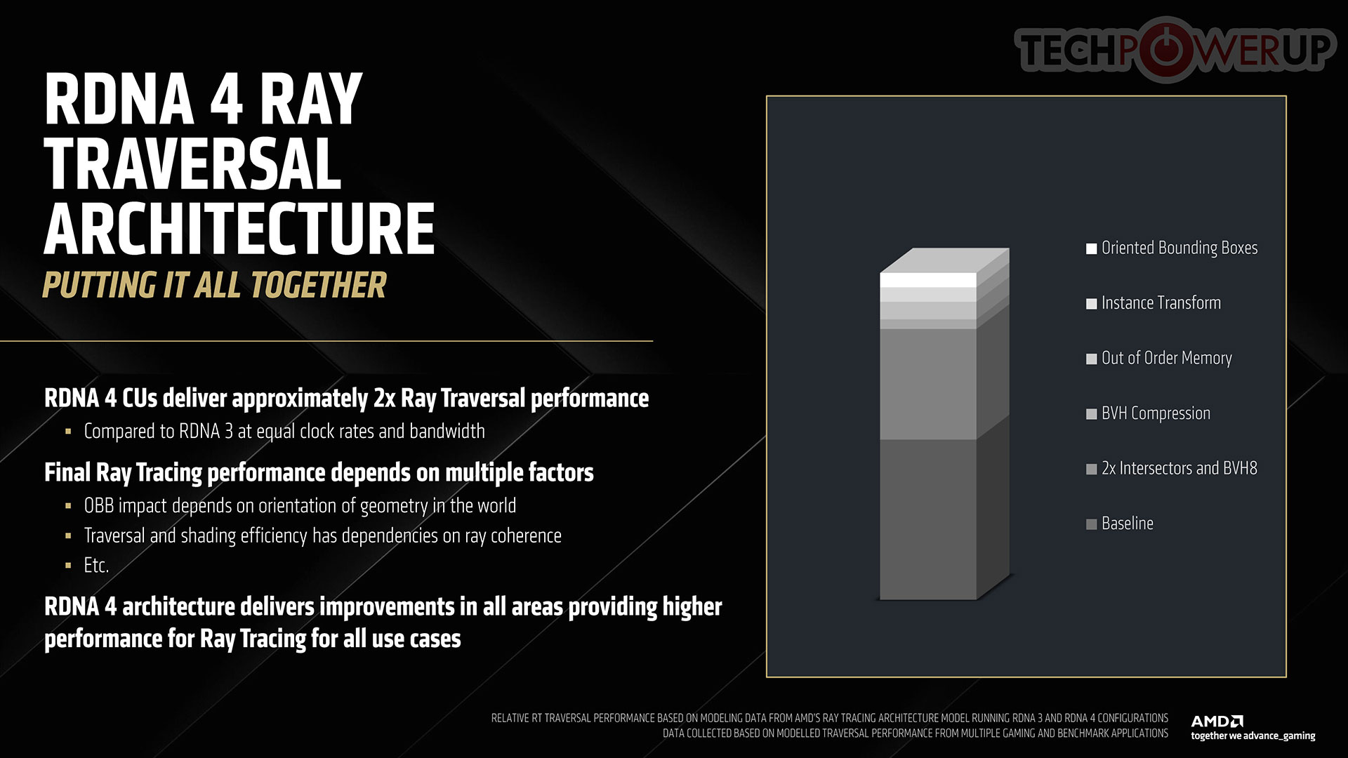
This graph highlights the contribution of various components toward the 100% generational ray traversal performance gain, allowing AMD to make do with a CU count of 64, with RDNA 3 being the baseline.
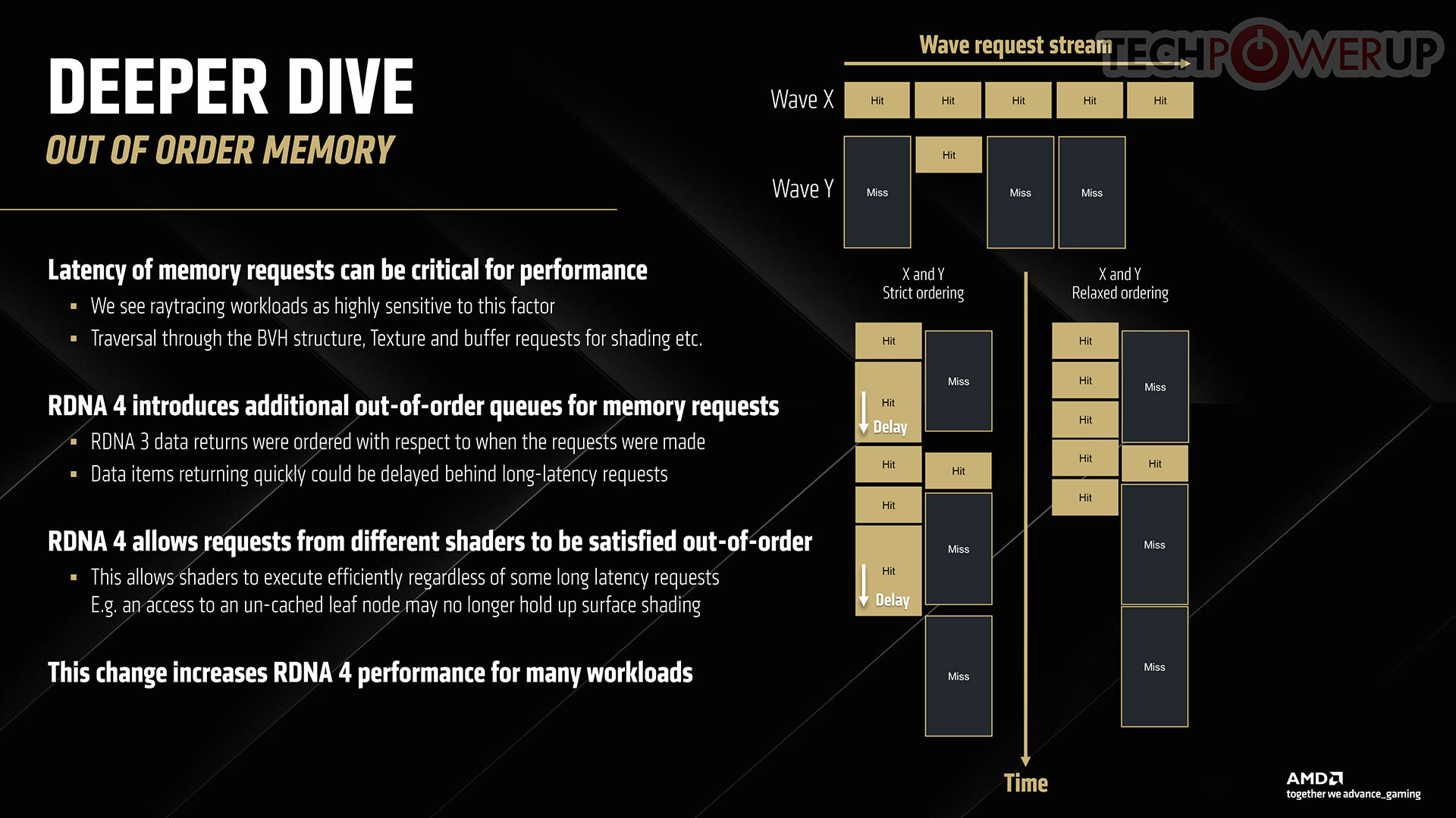
Both ray tracing and ML acceleration are memory sensitive applications, so AMD innovated a revolutionary change to its memory management system with the introduction of new out-of-order memory. All math is executed in waves on an RDNA GPU, and mutual dependencies between waves can cause memory request stream misses, as one wave's memory request queue waits for the other wave to complete its task. This is solved with a new out-of-order (relaxed ordering) memory management. This graph highlights the contribution of various components toward the 100% generational ray traversal performance gain, allowing AMD to make do with a CU count of 64, with RDNA 3 being the baseline.
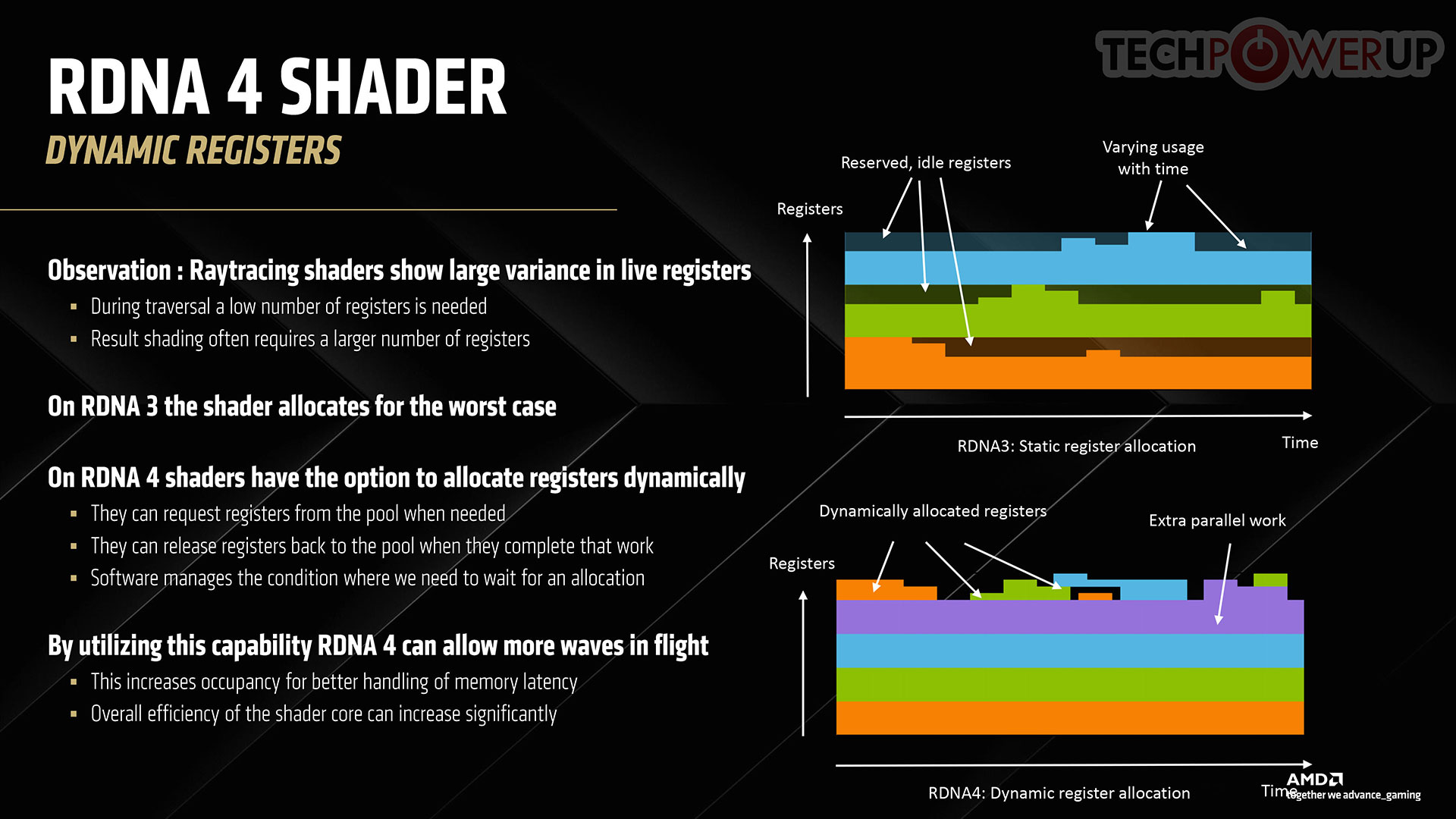
On AMD, a fairly big chunk of the ray tracing stack continues to be executed on shaders, but the company has made advances to ensure the cost of ray tracing on the shader resources of the GPU is minimal, with the introduction of Dynamic Registers to improve parallelism.
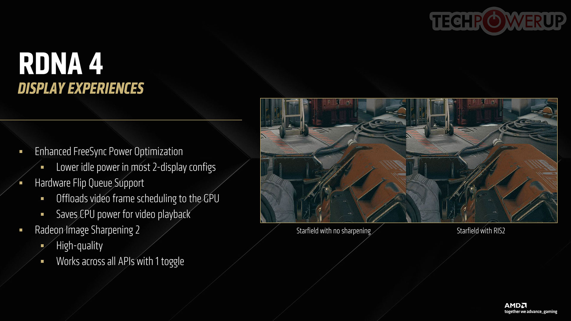
The new Radiance 2 Display Engine comes with major hardware updates that reduce GPU idle power draw in multi-monitor setups. The engine also comes with hardware flip-metering support (something NVIDIA also introduced with Blackwell, and which enables Multi-Frame Gen on the RTX 50-series). Flip-metering improves video frame pacing to the GPU and reduces CPU overhead for video playback. There is also a display engine level hardware image sharpening component that drives Radeon Image Sharpening. As for I/O, you get contemporary DisplayPort 2.1a and HDMI 2.1b, we are waiting to confirm the UHBR bit-rates.
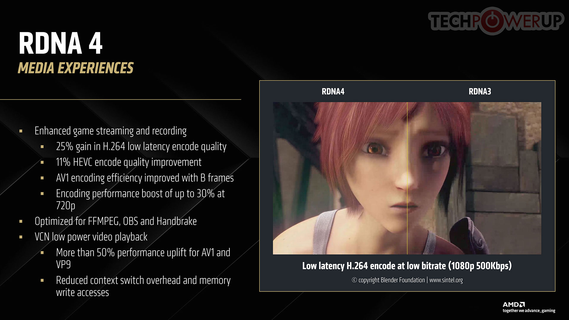
Navi 48 comes with a dual media engine, each of the two can perform concurrent encoding and decoding, and so the implementation resembles an NVIDIA GPU having two each of NVENC and NVDEC units. The new generation media engine offers a 25% increase in H.264 low-latency encode quality, and an 11% improvement in HEVC encode quality. AV1 encode and decode get B-frames support, vastly improving bitrates. A B-frame is a frame that lacks image information, but instead motion-vector values, that lets the decoder reconstruct the image component using past and future I-Frames (frames with image data). The media engine posts a 50% generational performance uplift (measured in encoder/decoder frame rates), with reductions in memory overhead.
Mar 6th, 2025 02:56 EST
change timezone
Latest GPU Drivers
New Forum Posts
- High-end build in the 2025 mad world situation (16)
- Oh boy here we go again...potential X3D woes (48)
- Cooling problems persist on LGA1700 (34)
- Rare GPUs / Unreleased GPUs (2042)
- I'm looking for a good tool to make the 3D scanning of my mini-pc using the photogrammetry and my Kinect 2. (1)
- Windows 11 General Discussion (5829)
- Extending wifi from a lousy router (32)
- Get 9070 or 9070 XT (28)
- I5 10300H undervolting ,need to stop thermal throttle (18)
- Flashing Rx7900xtx (0)
Popular Reviews
- Sapphire Radeon RX 9070 XT Nitro+ Review - Beating NVIDIA
- NVIDIA GeForce RTX 5070 Founders Edition Review
- ASUS Radeon RX 9070 TUF OC Review
- AMD Radeon RX 9070 Series Technical Deep Dive
- EIZO FlexScan EV4340X Review - A Multitasking Powerhouse
- RAWM ES21M Review
- ASUS GeForce RTX 5070 Ti TUF OC Review
- AMD Ryzen 7 9800X3D Review - The Best Gaming Processor
- MSI GeForce RTX 5070 Ti Vanguard SOC Review
- MSI GeForce RTX 5070 Ti Ventus 3X OC Review
Controversial News Posts
- NVIDIA GeForce RTX 50 Cards Spotted with Missing ROPs, NVIDIA Confirms the Issue, Multiple Vendors Affected (513)
- AMD Plans Aggressive Price Competition with Radeon RX 9000 Series (277)
- AMD Radeon RX 9070 and 9070 XT Listed On Amazon - One Buyer Snags a Unit (261)
- AMD Mentions Sub-$700 Pricing for Radeon RX 9070 GPU Series, Looks Like NV Minus $50 Again (248)
- NVIDIA Investigates GeForce RTX 50 Series "Blackwell" Black Screen and BSOD Issues (244)
- AMD RDNA 4 and Radeon RX 9070 Series Unveiled: $549 & $599 (241)
- AMD Radeon RX 9070 and 9070 XT Official Performance Metrics Leaked, +42% 4K Performance Over Radeon RX 7900 GRE (195)
- AMD Radeon RX 9070-series Pricing Leaks Courtesy of MicroCenter (158)