Mar 31st, 2025 01:40 EDT
change timezone
Latest GPU Drivers
New Forum Posts
- What is the latest game you finished or 100% (9)
- Help me decide if I should buy the arc B580 (As a backup) (0)
- Windows 10 Vs 11, Which one too choose? (127)
- What do you do for a living? (453)
- 5070 Ti power limit questions (25)
- Will you buy a RTX 5090? (461)
- WCG Daily Numbers (12820)
- Bluetooth to USB Conversion using a special circuit that I can create with my limited knowledge... (3)
- Alternatives to Autodesk Fusion 360 (4)
- Future-proofing my OLED (78)
Popular Reviews
- Sapphire Radeon RX 9070 XT Pulse Review
- ASRock Phantom Gaming B850 Riptide Wi-Fi Review - Amazing Price/Performance
- Samsung 9100 Pro 2 TB Review - The Best Gen 5 SSD
- Palit GeForce RTX 5070 GamingPro OC Review
- Sapphire Radeon RX 9070 XT Nitro+ Review - Beating NVIDIA
- Assassin's Creed Shadows Performance Benchmark Review - 30 GPUs Compared
- Enermax REVOLUTION D.F. 12 850 W Review
- AMD Ryzen 7 9800X3D Review - The Best Gaming Processor
- ASRock Radeon RX 9070 XT Taichi OC Review - Excellent Cooling
- XPG LEVANTE II 360 Review
Controversial News Posts
- AMD RDNA 4 and Radeon RX 9070 Series Unveiled: $549 & $599 (260)
- MSI Doesn't Plan Radeon RX 9000 Series GPUs, Skips AMD RDNA 4 Generation Entirely (142)
- Microsoft Introduces Copilot for Gaming (124)
- AMD Radeon RX 9070 XT Reportedly Outperforms RTX 5080 Through Undervolting (119)
- NVIDIA Reportedly Prepares GeForce RTX 5060 and RTX 5060 Ti Unveil Tomorrow (115)
- Over 200,000 Sold Radeon RX 9070 and RX 9070 XT GPUs? AMD Says No Number was Given (100)
- NVIDIA GeForce RTX 5050, RTX 5060, and RTX 5060 Ti Specifications Leak (96)
- Retailers Anticipate Increased Radeon RX 9070 Series Prices, After Initial Shipments of "MSRP" Models (90)
 28
28
Sapphire RX 7900 GRE Nitro+ Review
(28 Comments) »Introduction
Sapphire Radeon RX 7900 GRE Nitro+ is a premium custom design of AMD's performance segment graphics card that has eluded Western markets until now. The RX 7900 GRE (Golden Rabbit Edition) was originally conceived as a limited edition targeting the Chinese market, and was also available in Asian markets near China; but AMD has decided to give this a wider launch, if not a full global launch. It should be available in certain Western markets for purchase from tomorrow (February 27). This isn't a new GPU, with the earliest marketplace sightings of the card dating back to July 2023. Why then did AMD decide to give this card a wider launch now? This has to do with the January launch of NVIDIA's GeForce RTX 4070 Super and RTX 4070 Ti Super, which shook up the GPU market between $500 to $800.

The AMD Radeon RX 7800 XT launched at $550, with performance competitive to the then $600 RTX 4070, which caused its street price to trim down to around $580. The RTX 4070 Super convincingly beats the RX 7800 XT and displaces the RTX 4070 from its price, pushing it further down. This in turn forced the RX 7800 XT to settle around a $500 price point, creating a rather large gap between it and the RX 7900 XT. AMD already had the RX 7900 GRE carved up and selling on the Chinese market since July, so it was easy to just give it a wider launch.
AMD created the Radeon RX 7900 GRE by further cutting down the Navi 31 silicon which powers the RX 7900 XT and RX 7900 XTX. The company had created a smaller package substrate for the chip, so it could create RX 7900 series laptop GPUs with it. The smaller package helps in gaming notebooks where PCB real-estate is scarce. This package has a slimmer memory IO that's limited to 256-bit, and has fewer power pins than the regular Navi 31 package, so it enabled AMD to give the RX 7900 GRE more shaders than the RX 7800 XT, but with the same memory configuration, and a simpler board design than the RX 7900 XT.
To create the Radeon RX 7900 GRE, AMD enabled 80 out of 96 compute units (CU) on the graphics compute die (GCD), resulting in 5,120 stream processors, 160 AI accelerators, 80 Ray accelerators, and 320 TMUs. AMD also enabled 160 out of 192 ROPs available on the silicon. Just four of the six memory cache dies (MCDs) are enabled, each has a 16 MB segment of the GPU's Infinity Cache, and a 64-bit portion of the memory bus. Four of these add up to 64 MB Infinity Cache, and a 256-bit memory bus. AMD is using this to drive 16 GB of 18 Gbps GDDR6 memory, with 576 GB/s of bandwidth on tap—same as that of the RX 6950 XT. The total board power of the RX 7900 GRE is set at 260 W.
The RX 7900 GRE CU count may be close to that of the RX 7900 XT, which has 84, but the XT has other things going for it, such as a wider 320-bit memory bus driving 20 GB of 20 Gbps GDDR6 memory that works out to 38% higher memory bandwidth; besides all 192 ROPs being available. The RX 7800 XT may have a nearly identical memory configuration, but has 25% fewer shaders. So the RX 7900 GRE, on paper, is a nice halfway mark between the RX 7800 XT and RX 7900 XT. If it didn't cost more, this card could have been called something like the "RX 7900 XL," or simply the "RX 7900."
Driving the RX 7900 GRE is AMD's latest RDNA 3 graphics architecture, which is designed to get the most out of the 5 nm foundry node. The Navi 31 is the world's first chiplet-based gaming GPU. AMD identified specific components that benefit the most out of the switch to 5 nm, mainly the shader engines and front-end—and clumped them together on a centralized chiplet called the graphics compute die (GCD). All the components that don't benefit has much, namely the Infinity Cache and GDDR6 memory controllers, are broken apart into tiny chiplets called memory cache dies (MCDs), built on the slightly older 6 nm node. This way, AMD is able to increase its 5 nm wafer utilization. The chiplets are interconnected using Infinity Fanout Links, which make the seven chiplets work like one big chip. This is why the Navi 31 can't be called a multi-chip module: a package that has multiple chips that can otherwise exist on their own packages, but are made to share a package to conserve PCB footprint.
The new RDNA 3 Compute Unit supports dual-issue instruction rate compute units, support for new math formats, and a 17% increase in IPC over RDNA 2. The new AI accelerators, two per CU, prepare matrix math workloads for crunching by the stream processors, speeding up this process. The second generation AMD Ray accelerator uses several optimizations to increase ray intersection performance by 50% over the previous generation. There are other improvements, such as a decoupled GPU front-end, which runs at a higher clock speed than the Shader Engines. AMD also significantly updated the display engine to support DisplayPort 2.1 UHBR13, and HDMI 2.1; while the media engines are updated to support AV1 and HEVC encode and decode.
The Sapphire Nitro+ comes with a powerful cooling solution which appears to be carried over from the RX 7800 XT Nitro+. Both the RX 7800 XT and RX 7900 GRE have a nearly identical 260 W total board power, and an identical number of memory chips, so this cooler should perform similarly in both cards. The RX 7800 XT Nitro+ blew us away with massive overclocking potential, thanks in part to the cooler. This beast has a lot of aesthetic and functional features that should appeal to the gamer-streamer or enthusiast crowd, including plenty of RGB LED lighting. Sapphire is pricing the RX 7900 GRE at $600, which is a $50 premium over the AMD baseline and makes its price clash with the RTX 4070 Super.
Short 10-Minute Video Summary Comparing 6x RX 7900 GRE
Our goal with the videos is to create short summaries, not go into all the details and test results, which can be found in this written review.
| Price | Cores | ROPs | Core Clock | Boost Clock | Memory Clock | GPU | Transistors | Memory | |
|---|---|---|---|---|---|---|---|---|---|
| RTX 3070 | $310 | 5888 | 96 | 1500 MHz | 1725 MHz | 1750 MHz | GA104 | 17400M | 8 GB, GDDR6, 256-bit |
| RTX 3070 Ti | $350 | 6144 | 96 | 1575 MHz | 1770 MHz | 1188 MHz | GA104 | 17400M | 8 GB, GDDR6X, 256-bit |
| RX 6800 | $450 | 3840 | 96 | 1815 MHz | 2105 MHz | 2000 MHz | Navi 21 | 26800M | 16 GB, GDDR6, 256-bit |
| RX 7700 XT | $430 | 3456 | 96 | 2171 MHz | 2544 MHz | 2250 MHz | Navi 32 | 26500M | 12 GB, GDDR6, 192-bit |
| RX 6800 XT | $500 | 4608 | 128 | 2015 MHz | 2250 MHz | 2000 MHz | Navi 21 | 26800M | 16 GB, GDDR6, 256-bit |
| RTX 3080 | $450 | 8704 | 96 | 1440 MHz | 1710 MHz | 1188 MHz | GA102 | 28000M | 10 GB, GDDR6X, 320-bit |
| RTX 4070 | $525 | 5888 | 64 | 1920 MHz | 2475 MHz | 1313 MHz | AD104 | 35800M | 12 GB, GDDR6X, 192-bit |
| RX 7800 XT | $500 | 3840 | 96 | 2124 MHz | 2430 MHz | 2425 MHz | Navi 32 | 28100M | 16 GB, GDDR6, 256-bit |
| RX 6900 XT | $650 | 5120 | 128 | 2015 MHz | 2250 MHz | 2000 MHz | Navi 21 | 26800M | 16 GB, GDDR6, 256-bit |
| RX 6950 XT | $630 | 5120 | 128 | 2100 MHz | 2310 MHz | 2250 MHz | Navi 21 | 26800M | 16 GB, GDDR6, 256-bit |
| RTX 3090 | $800 | 10496 | 112 | 1395 MHz | 1695 MHz | 1219 MHz | GA102 | 28000M | 24 GB, GDDR6X, 384-bit |
| RTX 4070 Super | $590 | 7168 | 80 | 1980 MHz | 2475 MHz | 1313 MHz | AD104 | 35800M | 12 GB, GDDR6X, 192-bit |
| RX 7900 GRE | $550 | 5120 | 160 | 1880 MHz | 2245 MHz | 2250 MHz | Navi 31 | 57700M | 16 GB, GDDR6, 256-bit |
| Sapphire RX 7900 GRE Nitro+ | $600 | 5120 | 160 | 2052 MHz | 2391 MHz | 2250 MHz | Navi 31 | 57700M | 16 GB, GDDR6, 256-bit |
| RTX 4070 Ti | $720 | 7680 | 80 | 2310 MHz | 2610 MHz | 1313 MHz | AD104 | 35800M | 12 GB, GDDR6X, 192-bit |
| RTX 4070 Ti Super | $800 | 8448 | 112 | 2340 MHz | 2610 MHz | 1313 MHz | AD103 | 45900M | 16 GB, GDDR6X, 256-bit |
| RX 7900 XT | $700 | 5376 | 192 | 2000 MHz | 2400 MHz | 2500 MHz | Navi 31 | 57700M | 20 GB, GDDR6, 320-bit |
| RTX 3090 Ti | $1050 | 10752 | 112 | 1560 MHz | 1950 MHz | 1313 MHz | GA102 | 28000M | 24 GB, GDDR6X, 384-bit |
| RTX 4080 | $1200 | 9728 | 112 | 2205 MHz | 2505 MHz | 1400 MHz | AD103 | 45900M | 16 GB, GDDR6X, 256-bit |
| RTX 4080 Super | $1300 | 10240 | 112 | 2295 MHz | 2550 MHz | 1438 MHz | AD103 | 45900M | 16 GB, GDDR6X, 256-bit |
| RX 7900 XTX | $910 | 6144 | 192 | 2300 MHz | 2500 MHz | 2500 MHz | Navi 31 | 57700M | 24 GB, GDDR6, 384-bit |
| RTX 4090 | $1850 | 16384 | 176 | 2235 MHz | 2520 MHz | 1313 MHz | AD102 | 76300M | 24 GB, GDDR6X, 384-bit |
AMD RDNA 3 Graphics Architecture


The Radeon RX 7900 series debuts AMD's 3rd generation RDNA graphics architecture, termed RDNA 3. With it, AMD plans to repeat the generational 50% performance/Watt gain it achieved with RDNA 2, which sprung it back to the high-end graphics segment after a long gap. AMD claims it succeeded in this endeavor, with a 54% generational performance/Watt gain. At the heart of this effort is the switch to the new TSMC 5 nm EUV foundry node. AMD figured out early on that it cannot build large monolithic GPUs on 5 nm without thinning its margins in the fight against NVIDIA, and set out to innovate the Chiplet architecture for the GPU. Under this, specific parts of the GPU that actually benefit from a switch to a newer foundry node, such as the Shader Engines, would be built on a centralized 5 nm die called the Graphics Compute Die (GCD), while those components that can make do with a less advanced node, namely the memory controllers and L3 cache, would be spun off to chiplets called Memory Cache Dies (MCDs), built on 6 nm.


The "Navi 31" GPU is hence a chiplet GPU and not a multi-chip module like "Vega 10." In a chiplet-based device, various components that can otherwise not exist on their own packages, are placed on a single package, with the goal of minimizing production costs, by stratifying their need for a new foundry node, such that only the most power-intensive IP receive the most advanced node. In a MCM, chips that can otherwise exist on their own package, are combined onto a single package for conserving PCB real-estate, or reducing latency. The GCD in the "Navi 31" GPU hence has all the shader engines, caches up to L2, the front-end Command Processor, Async Compute Engines (ACEs), the Display Engine, and the Media Engine. Each of the six MCDs has a 64-bit wide memory bus, and a 16 MB segment of the GPU's 96 MB Infinity Cache memory. The size of the Infinity Cache may have been generationally reduced (compared to 128 MB on "Navi 21"), but AMD has widened the memory bus itself, from 256-bit up to 384-bit, however the GRE makes do with 256-bit due to the design changes outlined earlier.


Much of the architectural innovation is not with the chiplet design (a packaging innovation); but at the level of the RDNA 3 Dual-Compute Unit (or Compute Unit pair). The "Navi 31" GPU physically features 96 compute units spread across six Shader Engines. AMD claims that at the same engine clocks, the RDNA 3 CU offers a 17.4% IPC increase over the RDNA 2 CU. There are 20% more CUs over the "Navi 21," and these run at higher engine clocks, tapping into the power headroom afforded by the 5 nm process. These combined work out to the 54% generational performance uplift, with which AMD plans to retain competitiveness with NVIDIA's RTX 40-series "Ada" high-end SKUs.


The new RDNA 3 CU introduces multi-precision capability for the 64 stream processors per CU: operating either as 1x SIMD64 or 2x SIMD32 units. The Vector Unit that houses these SIMD units can either function as a SIMD execution mechanism, or as a Matrix execution unit, thanks to the new AI Matrix Accelerator, which provides a 2.7x matrix multiplication performance uplift versus conventional SIMD execution. Also added are support for the Bfloat16 instruction-set, and SIMD8 execution. The GPU hence enjoys AI hardware-acceleration that can be leveraged in future feature-additions relevant to gamers, such as FSR 3.0. Game developers will also look for ways to exploit accelerated AI, now that all three brands feature it (NVIDIA Tensor cores and Intel XMX cores).
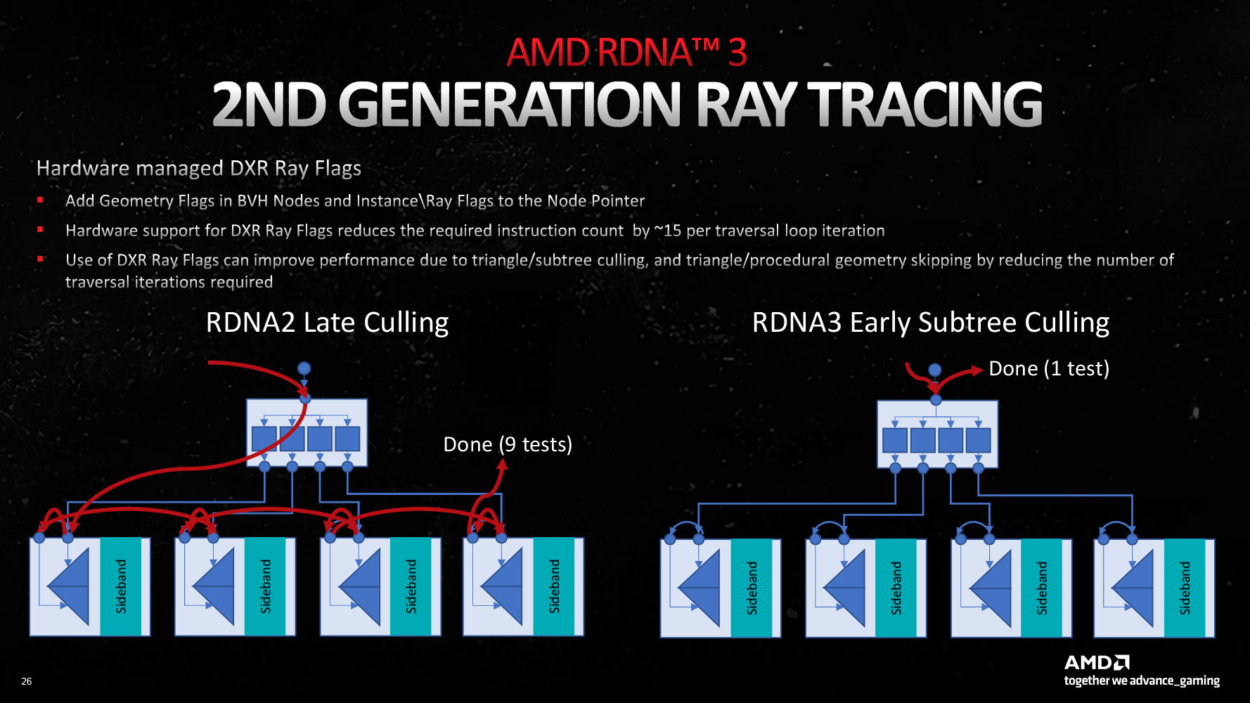

AMD's first-generation Ray Accelerator, introduced with the RDNA 2 architecture, was the result of a hasty effort to catch up to NVIDIA with a DirectX 12 Ultimate GPU, where they developed a fixed-function hardware to calculate ray intersections, and offloaded a large chunk of RT processing to the generationally-doubled SIMD resources. With RDNA 3, they've refined the Ray Accelerator to achieve an 80% ray tracing performance uplift over the previous generation, when you add up the Ray Accelerator count, their higher engine clocks, and other hardware-level optimizations, such as early subtree culling, specialized box sorting modes, and reduced traversal iterations.


There is a 50% ray intersection capacity improvement for the "Navi 31" GPU thanks to these optimizations, and cycles-per-ray reduction. Besides these, AMD has also made several improvements to the geometry- and pixel-pipes, with the introduction of the new multi-draw indirect accelerator (MDIA), which reduces CPU API and driver-level overheads by gathering and parsing of multi-draw command data. At the hardware-level 12 primitives per clock is now supported compared to 8 per clock on RDNA 2, thanks to culling. The core-configuration overall enables 50% more rasterized performance per clock.
The GCD features six Shader Engines, each with 16 compute units (or 8 dual compute units), which work out to 1,024 stream processors. Six such Shader Engines make up 6,144 stream processors with 96 Ray Accelerators and 96 AI Accelerators. The GPU has 384 TMUs, and a massive 192 ROPs—a 50% increase over "Navi 21." The Radeon RX 7900 XTX enables all 96 CUs, and maxes out the silicon, whereas the RX 7900 XT has 84 out of 96 CUs enabled, which work out to 5,376 stream processors, 84 Ray Accelerators, 336 TMUs, and an unchanged 192 ROPs. The new RX 7900 GRE has 80 CUs enabled, which work out to 5,120 stream processors, 80 Ray Accelerators, 320 TMUs, and 160 ROPs. The RX 7900 XTX gets 24 GB of GDDR6 memory across the GPU's entire 384-bit memory bus, with a memory speed of 20 Gbps (GDDR6-effective), which means 960 GB/s of memory bandwidth. The RX 7900 XT is equipped with 20 GB of memory across a narrower 320-bit memory bus carved out by disabling one of the six MCDs. At the same 20 Gbps speed, this yields 800 GB/s bandwidth. The RX 7900 GRE goes one further step down, with two of the six MCDs being disabled, for a 256-bit memory bus, running 16 GB of memory at 18 Gbps speed, for 576 GB/s of bandwidth.
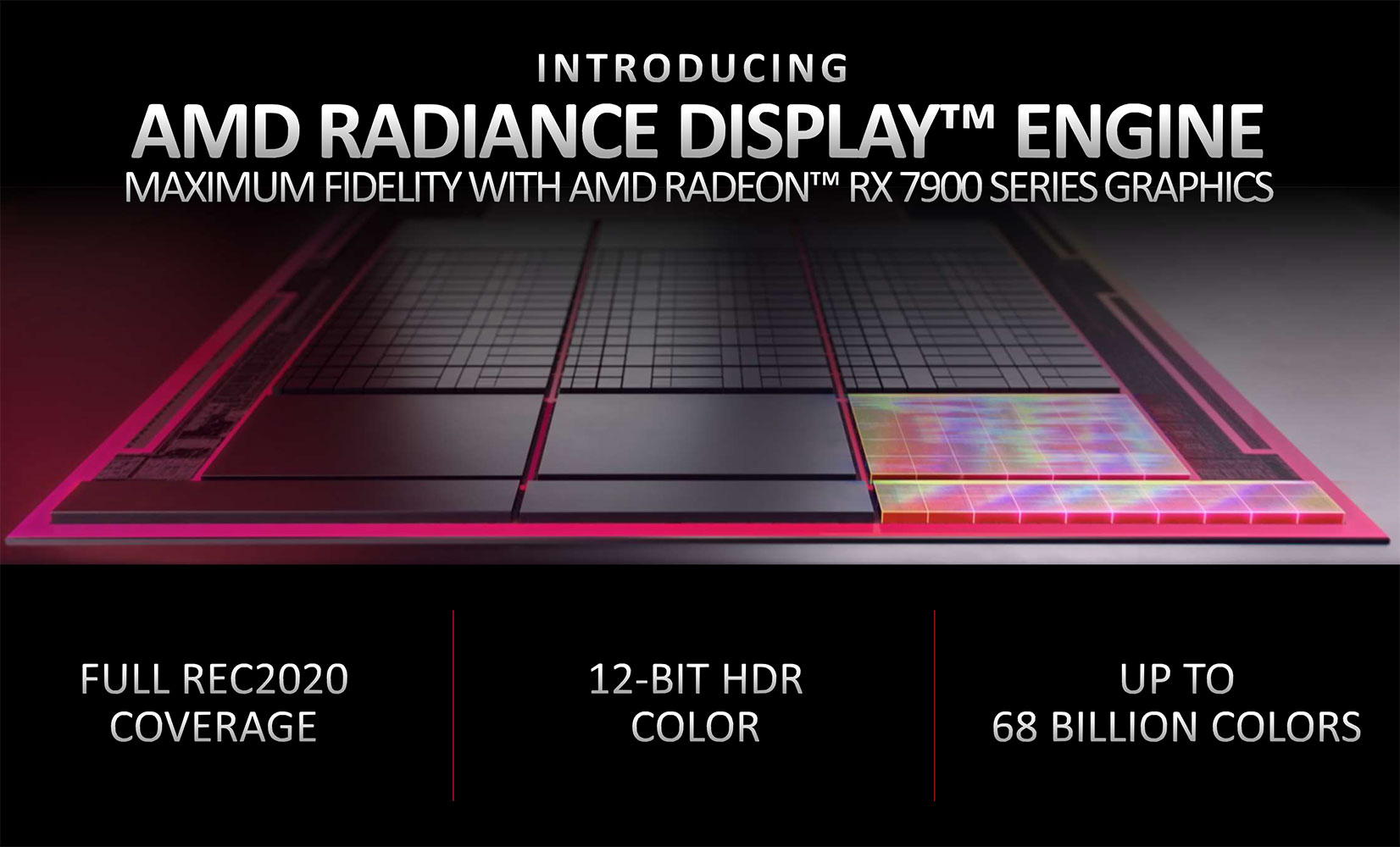

AMD has significantly improved the Display Engine of "Navi 31" over the previous-generation in terms of connectivity. The new Radiance Display Engine comes with native support for DisplayPort 2.1, which enables 8K output at up to 165 Hz refresh-rate, or 4K at up to 480 Hz, with a single cable. AMD has refined its FSR 2 algorithm to support 8K (i.e. render at a lower resolution with FSR-enhanced upscaling), to make it possible to enjoy the latest AAA titles at playable frame-rates on 8K displays. Both the RX 7900 series cards get two full-size DP 2.1 connectors, besides an HDMI 2.1b, and a USB-C with DP 1.2 passthrough. The "Navi 31" silicon receives full hardware-accelerated AV1 encode and decode capabilities, through dual independent encode/decoders, so two independent video streams can be simultaneously transcoded, or one stream at twice the framerate. With this generation, AMD is also introducing SmartAccess Video, a feature that lets the AMD driver leverage the hardware encoders of the RDNA 2 iGPU of Ryzen 7000 desktop processors, for additional encoding performance.
FidelityFX SuperResolution 3 Fluid Motion Frames (FSR 3 and FMF)

AMD announced the much awaited FidelityFX Super Resolution 3 and Fluid Motion Frames. FSR 3 is being announced as a technological rival to NVIDIA DLSS 3 Frame Generation. The premise with both technologies is the same—to effectively double frame-rates by generating alternate frames without running them through the entire graphics rendering pipeline, it's just that the two technologies differ in their approach to this goal.
FSR 3 builds on FSR 2 with its updated super resolution upscaler promising generational quality improvements at every given rendering resolution. Fluid Motion Frames (FMF) isn't the entirety of the FSR 3 feature-set, but is its most important feature-addition. FMF is a frame interpolation technology much like the one consumer televisions come with. Alternate frames are generated as an approximate of two frames. Where FMF differs from DLSS 3 Frame Generation is that while NVIDIA uses a hardware component called optical flow accelerator and the GPU's AI acceleration to generate an intermediate frame without involving the graphics rendering pipeline, FMF uses a certain amount of the graphics rendering pipeline. At a hardware level, FMF uses the main SIMD machinery of the GPU, leveraging asynchronous compute. As with DLSS 3 FG, FSR 3 FMF comes with added latency. NVIDIA counteracts this with Reflex, while AMD uses Radeon AntiLag+. Both technologies try to keep the frame queue short to reduce whole system latencies.
One major advantage FSR 3 FMF enjoys over DLSS 3 FG is that it works on any modern DirectX 12 GPU that supports async compute, since it doesn't require a specific hardware component the way DLSS 3 FG requires the Optical Flow Accelerator on NVIDIA "Ada" GPUs. The only limiting factor here is the performance. To be more specific, AMD says that all Radeon GPUs from RX 5700 series onward; and all GeForce GPUs from RTX 20-series onward, should support FSR 3 FMF. Also, FSR 3 FMF is as easy to integrate with games as FSR 2 is. The first games implementing FSR 3 FMF should arrive in Fall 2023. AMD is also working to extend FMF to Radeon Super Resolution, the driver-level technology that enables performance upscaling to even games that don't support FSR.
HYPR-RX

HYPR-RX is an interesting new feature in the AMD Software (control center) application. It is a one-click performance boosting technology that works with any DirectX 11 or DirectX 12 game. The software is a cocktail of Radeon Boost, Radeon AntiLag+, and Radeon Super Resolution, and applies the three features on any running game as needed, automatically. Radeon Boost improves performance by dynamically reducing the render resolution of a game when there's too much motion on the screen (and hence not enough detail needed). Radeon Super Resolution improves frame-rates as it applies FSR on the output of a game rendered at a lower resolution (including the frames lowered in resolution by Radeon Boost. AntiLag+ counteracts the latency added by these two, by shortening the frame queue. AFMF is part of the HYPR-RX feature-set, which can be activated with a single click.
Packaging


The Card


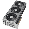
For their RDNA 3 Radeon RX 7000 Series of graphics cards, Sapphire has come up with a completely new design. The main color is a matte gray that looks stunning. I love the looks of the main cooler, it's almost like it came right out of Apple's design labs. The metal backplate is a bit more busy, with various cutouts, logos and labels.


Dimensions of the card are 32.0 x 13.5 cm, and it weighs 1600 g.


Installation requires three slots in your system.

Display connectivity includes two standard DisplayPort 2.1 ports (RDNA 2 had 1.4a) and two HDMI 2.1a (same as RDNA 2).
AMD has upgraded their encode/decode setup. It now comes with two independent hardware units that can encode and decode two streams of video in parallel, or one stream at double the FPS rate. There's support for VP9, H.264, H.265 and AV1 decode, and encoding is supported for H.264, H.265 and AV1.

The card uses a classic dual 8-pin together with PCIe slot power input config, rated for 375 W maximum power. NVIDIA on the other hand uses the new 12+4 pin ATX 12V-2x6 connector, which is rated for up to 600 W of power draw.

This dual BIOS switch lets you toggle between the default BIOS and a "quiet" BIOS, which runs the fans at a more relaxed fan curve.
With this generation, Sapphire is including their software BIOS switch feature, too. The BIOS switch has three positions: left-most = default BIOS, middle = secondary BIOS, right = software-controlled. In Sapphire's TRIXX software you can now toggle the BIOS selection, without having to open your case or crawl under your desk.

Near the back of the card, Sapphire has placed an ARGB output that lets you sync the rest of the system to the RGB effects of your graphics card. Here you also get a 4-pin header for a case fan that runs synced with the graphics card fan speed. The "Fan In" label is misleading, I would have called it "Fan Out," or "External Fan."
Our Patreon Silver Supporters can read articles in single-page format.
Mar 31st, 2025 01:40 EDT
change timezone
Latest GPU Drivers
New Forum Posts
- What is the latest game you finished or 100% (9)
- Help me decide if I should buy the arc B580 (As a backup) (0)
- Windows 10 Vs 11, Which one too choose? (127)
- What do you do for a living? (453)
- 5070 Ti power limit questions (25)
- Will you buy a RTX 5090? (461)
- WCG Daily Numbers (12820)
- Bluetooth to USB Conversion using a special circuit that I can create with my limited knowledge... (3)
- Alternatives to Autodesk Fusion 360 (4)
- Future-proofing my OLED (78)
Popular Reviews
- Sapphire Radeon RX 9070 XT Pulse Review
- ASRock Phantom Gaming B850 Riptide Wi-Fi Review - Amazing Price/Performance
- Samsung 9100 Pro 2 TB Review - The Best Gen 5 SSD
- Palit GeForce RTX 5070 GamingPro OC Review
- Sapphire Radeon RX 9070 XT Nitro+ Review - Beating NVIDIA
- Assassin's Creed Shadows Performance Benchmark Review - 30 GPUs Compared
- Enermax REVOLUTION D.F. 12 850 W Review
- AMD Ryzen 7 9800X3D Review - The Best Gaming Processor
- ASRock Radeon RX 9070 XT Taichi OC Review - Excellent Cooling
- XPG LEVANTE II 360 Review
Controversial News Posts
- AMD RDNA 4 and Radeon RX 9070 Series Unveiled: $549 & $599 (260)
- MSI Doesn't Plan Radeon RX 9000 Series GPUs, Skips AMD RDNA 4 Generation Entirely (142)
- Microsoft Introduces Copilot for Gaming (124)
- AMD Radeon RX 9070 XT Reportedly Outperforms RTX 5080 Through Undervolting (119)
- NVIDIA Reportedly Prepares GeForce RTX 5060 and RTX 5060 Ti Unveil Tomorrow (115)
- Over 200,000 Sold Radeon RX 9070 and RX 9070 XT GPUs? AMD Says No Number was Given (100)
- NVIDIA GeForce RTX 5050, RTX 5060, and RTX 5060 Ti Specifications Leak (96)
- Retailers Anticipate Increased Radeon RX 9070 Series Prices, After Initial Shipments of "MSRP" Models (90)