 8
8
Seagate FireCuda 510 1 TB Review
Test Setup »The Drive
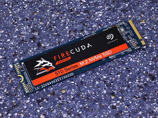
The drive uses the M.2 2280 form factor, which makes it 22 mm wide and 80 mm long.
Like most M.2 NVMe SSDs, the Seagate FireCuda 510 connects to the host system over a PCI-Express 3.0 x4 interface.
On the PCB, you'll find four flash chips, the controller, and two DRAM chips.
Seagate rebranded a Phison PS5012-E12 controller; it uses eight flash channels and supports 3D TLC, QLC, and PCI-Express 3.0 x4. It is produced on a 28 nm process at TSMC Taiwan.
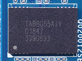
The four TLC flash chips are made by Toshiba, built using 64-layers on a 15 nanometer 3D NAND production process.
Two SKhynix DDR4-2400 chips provide a total of 1 GB of fast DRAM storage for the controller to store the mapping tables in.
Jun 30th, 2025 17:31 CDT
change timezone
Latest GPU Drivers
New Forum Posts
- Help me choose the right PSU , Cooler Master vs Seasonic (53)
- HOW TO ADD NVMe M.2 SSD SUPPORT TO OLD MOTHERBOARDS WITH AWARD-Phoenix LEGACY SUPPORT? (2)
- Whats a fair asking price - MSI 4070 Super (4)
- HTPC Power Consumption Discussion, Upgrade vs Migration (18)
- RX 9000 series GPU Owners Club (1103)
- Will you buy a RTX 5090? (579)
- Rare GPUs / Unreleased GPUs (2111)
- Steam Deck Owners Clubhouse (530)
- Can you guess Which game it is? (193)
- Good time in the year to buy a new PC (4)
Popular Reviews
- Sapphire Radeon RX 9070 XT Nitro+ Review - Beating NVIDIA
- ASUS ROG Crosshair X870E Extreme Review
- Sapphire Radeon RX 9060 XT Pulse OC 16 GB Review - Samsung Memory Tested
- Lexar NQ780 4 TB Review
- AVerMedia CamStream 4K Review
- ASRock Phantom Gaming Z890 Riptide Wi-Fi Review
- AMD Ryzen 7 9800X3D Review - The Best Gaming Processor
- Upcoming Hardware Launches 2025 (Updated May 2025)
- Intel Core Ultra 7 265K Review
- NVIDIA GeForce RTX 5060 8 GB Review
TPU on YouTube
Controversial News Posts
- Intel's Core Ultra 7 265K and 265KF CPUs Dip Below $250 (288)
- NVIDIA Grabs Market Share, AMD Loses Ground, and Intel Disappears in Latest dGPU Update (204)
- Some Intel Nova Lake CPUs Rumored to Challenge AMD's 3D V-Cache in Desktop Gaming (140)
- Microsoft Partners with AMD for Next-gen Xbox Hardware (105)
- NVIDIA Launches GeForce RTX 5050 for Desktops and Laptops, Starts at $249 (104)
- Intel "Nova Lake‑S" Series: Seven SKUs, Up to 52 Cores and 150 W TDP (100)
- NVIDIA GeForce RTX 5080 SUPER Could Feature 24 GB Memory, Increased Power Limits (89)
- Reviewers Bemused by Restrictive Sampling of RX 9060 XT 8 GB Cards (88)


