Tuesday, May 25th 2021

AMD "Milan-X" Processor Could Use Stacked Dies with X3D Packaging Technology
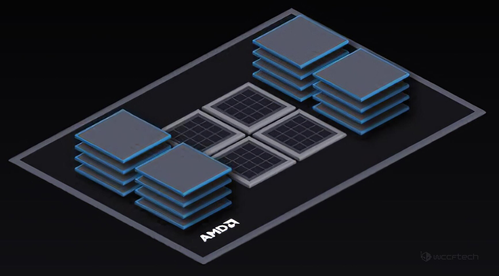
AMD is in a constant process of processor development, and there are always new technologies on the horizon. Back in March of 2020, the company has revealed that it is working on new X3D packaging technology, that integrated both 2.5D and 3D approaches to packing semiconductor dies together as tightly as possible. Today, we are finally getting some more information about the X3D technology, as we have the first codename of the processor that is featuring this advanced packaging technology. According to David Schor, we have learned that AMD is working on a CPU that uses X3D tech with stacked dies, and it is called Milan-X.
The Milan-X CPU is AMD's upcoming product designed for data center usage. The rumors suggest that the CPU is designed for heavy bandwidth and presumably a lot of computing power. According to ExecutableFix, the CPU uses a Genesis-IO die to power the connectivity, which is an IO die from EPYC Zen 3 processors. While this solution is in the works, we don't know the exact launch date of the processor. However, we could hear more about it in AMD's virtual keynote at Computex 2021. For now, take this rumor with a grain of salt.
Sources:
Patrick Schur, ExecutableFix, via VideoCardz
The Milan-X CPU is AMD's upcoming product designed for data center usage. The rumors suggest that the CPU is designed for heavy bandwidth and presumably a lot of computing power. According to ExecutableFix, the CPU uses a Genesis-IO die to power the connectivity, which is an IO die from EPYC Zen 3 processors. While this solution is in the works, we don't know the exact launch date of the processor. However, we could hear more about it in AMD's virtual keynote at Computex 2021. For now, take this rumor with a grain of salt.
10 Comments on AMD "Milan-X" Processor Could Use Stacked Dies with X3D Packaging Technology
That glue is Illegal and i don't accept the result of this election #notmyglue #MakeProcessorsGreatAgain
Jokes Aside, looks cool i hope it doens't come at a latency cost or huge power draw/temps, but its for servers so they can figure it out a way to cool it.
I bet this is how we'll get 128+-core Threadrippers.
"Threadripper 6990X, 256 cores, 512 threads, up to 4TB of DDR5 RAM in 16-channel, PCIe 6.0, MSRP $6000"
Do we will see actual high clock or it will be a 256 core/32 chiplets 1 GHz low voltage CPU. can't wait to see how this will behave. Even if this can be taken with a grain of salt, we will see stacked chips in the near future.
They use traces to remove the heat from those area's. IBM did even experiment with such traces basicly providing watercooling on nm level.
Ofcourse you can go high clocks; it's just a bit of impossible task when working with 64 cores and beyond. For high clocks you need a less dense chip if you want to preserve power consumption and / or cooling.
Ramping up clockspeed requires more voltage, and since the power is proportional to the scale of the voltage, a fast and narrow solution will always be less efficient than a (fully-utilised) slow and wide solution. That's Datacenter 101.
but we will see, still unclear what these dies will be. It's not unlikely that wit would be HBM or something else.
That article seemed to refer to that diagram as four compute chiplets and the stacks being HBM memory, similar to a CPU version of the Vega/Radeon VII GPU designs. Cooling an HBM stack is probably less challenging than trying to cool a stack of CPU chiplets clocked to a high frequency.
Perhaps the HBM could act as a form of L4 cache, similar to what Intel did with Broadwell's eDRAM?
The latest greatest 40-core Intel® Xeon® Platinum 8380 Processor (60M Cache, 2.30 GHz) is $6743.00 MSRP, or $168.57/core. 9282 is $13012 for 56 cores ($232.35/core) but that’s a precious-gen product so forget it. 256 cores for $60k would be an easy sell for 2U2P and a game-changer for density. Doing it in 1U2P or smaller blade systems would be just incredible.
But i think this will happen in the near future. This is the next big thing. I do not thing we will see a Server CPU with HBM. But i could see a custom chips with as much as possible cores + HBM to be put in a HPC chip for a future super-computer doing massive AVX-512 calculation while remaining as power efficient as possible.