News Posts matching #4 nm

Return to Keyword Browsing

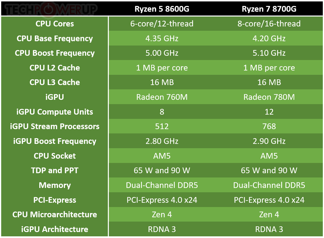
Samsung Electronics Announces First Quarter 2024 Results

Samsung Electronics today reported financial results for the first quarter ended March 31, 2024. The Company posted KRW 71.92 trillion in consolidated revenue on the back of strong sales of flagship Galaxy S24 smartphones and higher prices for memory semiconductors. Operating profit increased to KRW 6.61 trillion as the Memory Business returned to profit by addressing demand for high value-added products. The Mobile eXperience (MX) Business posted higher earnings and the Visual Display and Digital Appliances businesses also recorded increased profitability.

The weakness of the Korean won against major currencies resulted in a positive impact on company-wide operating profit of about KRW 0.3 trillion compared to the previous quarter. The Company's total capital expenditures in the first quarter stood at KRW 11.3 trillion, including KRW 9.7 trillion for the Device Solutions (DS) Division and KRW 1.1 trillion on Samsung Display Corporation (SDC). Spending on memory was focused on facilities and packaging technologies to address demand for High Bandwidth Memory (HBM), DDR5 and other advanced products, while foundry investments were concentrated on establishing infrastructure to meet medium- to long-term demand. Display investments were mainly made in IT OLED products and flexible display technologies.

AMD Readies Ryzen 7 8700F and Ryzen 5 8400F for Retail Channel Launch

AMD is reportedly planning to launch the Ryzen 7 8700F and Ryzen 5 8400F Socket AM5 desktop processors for a global launch, in the retail channel, as boxed processors. The two chips had launched earlier this month in the Chinese retail market. The 8700F reportedly comes with an OPN of 100-100001590BOX, while the 8400F is marked 100-100001591BOX. The "F" in both SKUs denotes a lack of integrated graphics. The Ryzen 7 8700F is an 8-core/16-thread processor based on the 4 nm "Hawk Point" silicon, while the 8400F is a 6-core/12-thread processor based on "Phoenix 2," which offers two "Zen 4" cores that run at higher clock speeds, and four "Zen 4c" cores that run at lower speeds.

The lack of an iGPU isn't the only thing differentiating the 8700F from the 8700G, the new chip even comes with slightly lower CPU clock speeds—100 MHz lower base and maximum boost frequencies. The 8700F CPU runs at a base frequency of 4.10 GHz, with 5.00 GHz maximum boost, when compared to the 4.20/5.10 GHz speeds of the 8700G. The 8400F, on the other hand, runs at 4.20 GHz base frequency, and a 4.70 GHz maximum boost frequency that applies to at least its two "Zen 4" cores; its four "Zen 4c" cores run at lower frequencies. There is no word on pricing. One reason you could want an 8700F over something like a 7700 would be its appetite for memory overclocking, if you can overlook the lack of integrated graphics, a smaller L3 cache, and most importantly, the lack of PCIe Gen 5, and four fewer PCIe lanes.

Samsung Signs $3 Billion HBM3E 12H Supply Deal with AMD

Korean media reports that Samsung Electronics has signed a 4.134 trillion Won ($3 billion) agreement with AMD to supply 12-high HBM3E stacks. AMD uses HBM stacks in its AI and HPC accelerators based on its CDNA architecture. This deal is significant, as it gives analysts some idea of the kind of volumes of AI GPUs AMD is preparing to push into the market, if they know what percent of an AI GPU's bill of materials is made up by memory stacks. AMD has probably negotiated a good price for Samsung's HBM3E 12H stacks, given that rival NVIDIA almost exclusively uses HBM3E made by SK Hynix.

The AI GPU market is expected to heat up with the ramp of NVIDIA's "Hopper" H200 series, the advent of "Blackwell," AMD's MI350X CDNA3, and Intel's Gaudi 3 generative AI accelerator. Samsung debuted its HBM3E 12H memory in February 2024. Each stack features 12 layers, a 50% increase over the first generation of HBM3E, and offers a density of 36 GB per stack. An AMD CDNA3 chip with 8 such stacks would have 288 GB of memory on package. AMD is expected to launch the MI350X in the second half of 2024. The star attraction with this chip is its refreshed GPU tiles built on the TSMC 4 nm EUV foundry node. This seems like the ideal product for AMD to debut HBM3E 12H on.

AMD Expands Commercial AI PC Portfolio to Deliver Leadership Performance Across Professional Mobile and Desktop Systems

Today, AMD announced new products that will expand its commercial mobile and desktop AI PC portfolio, delivering exceptional productivity and premium AI and connectivity experiences to business users. The new AMD Ryzen PRO 8040 Series are the most advanced x86 processors built for business laptops and mobile workstations. In addition, AMD also announced the AMD Ryzen PRO 8000 Series desktop processor, the first AI enabled desktop processor for business users, engineered to deliver cutting-edge performance with low power consumption.

With AMD Ryzen AI built into select models, AMD is further extending its AI PC leadership. By leveraging the CPU, GPU, and dedicated on-chip neural processing unit (NPU), new Ryzen AI-powered processors provide more dedicated AI processing power than previous generations, with up to 16 dedicated NPU TOPS (Trillions of Operations Per Second) and up to 39 total system TOPS. Commercial PCs equipped with new Ryzen AI-enabled processors will help transform user experience, offering next-gen performance for AI-enabled collaboration, content creation, and data and analytics workloads. With the addition of AMD PRO technologies, IT managers can unlock enterprise-grade manageability features to simplify IT operations and complete PC deployment faster across the organization, built-in security features for chip-to-cloud defense from sophisticated attacks, as well as unprecedented stability, reliability and platform longevity for enterprise software.

US Backs TSMC's $65B Arizona Investment with $11.6B Support Package

According to the latest report from Bloomberg, the US government under Joe Biden's administration has announced plans to provide Taiwan Semiconductor Manufacturing Company (TSMC) with a substantial financial support package worth $11.6 billion. The package is composed of $6.6 billion in grants and up to $5 billion in loans. This represents the most significant financial assistance approved under the CHIPS and Science Act, a key initiative to resurrect the US chip industry. The funding will aid TSMC in establishing three cutting-edge semiconductor production facilities in Arizona, with the company's total investment in the state expected to exceed an impressive $65 billion. TSMC's multi-phase Arizona project will commence with the construction of a fab module near its existing Fab 21 facility. Production using 4 nm and 5 nm process nodes is slated to begin by early 2025. The second phase, scheduled for 2028, will focus on even more advanced 2 nm and 3 nm technologies.

TSMC has kept details about the third facility's production timeline and process node under wraps. The company's massive investment in Arizona is expected to profoundly impact the local economy, creating 6,000 high-tech manufacturing jobs and over 20,000 construction positions. Moreover, $50 million has been earmarked for training local workers, which aligns with President Joe Biden's goal of bolstering domestic manufacturing and technological independence. However, TSMC's Arizona projects have encountered obstacles, including labor disputes and uncertainties regarding government support, resulting in delays for the second facility's production timeline. Additionally, reports suggest that at least one TSMC supplier has abandoned plans to set up operations in Arizona due to workforce-related challenges.

AMD Launches Ryzen Embedded 8000 Series Processors with Integrated NPUs for Industrial AI

AMD has introduced the Ryzen Embedded 8000 Series processors, the first AMD embedded devices to combine NPUs based on the AMD XDNA architecture with traditional CPU and GPU elements, optimized for workload versatility and adaptability targeting industrial AI applications. Embedded solution engineers and developers can harness the processing power and leadership features for a variety of industrial AI applications including machine vision, robotics, and industrial automation. AI is widely used in machine vision applications today to enhance quality control and inspection processes.

AI can also help robots make real-time, route-planning decisions and adapt to dynamic environments. In industrial automation, AI processing helps intelligent edge devices perform complex analysis and decision-making without relying on cloud connectivity. This allows for real-time monitoring, predictive maintenance, and autonomous control of industrial processes, enhancing operational efficiency and reducing downtime.

Nvidia CEO Reiterates Solid Partnership with TSMC

One key takeaway from the ongoing GTC is that Nvidia's AI empire has taken shape with strong partnerships from TSMC and other Taiwanese makers, such as those major server ODMs.

According to the news report from the technology-focused media DIGITIMES Asia, during his keynote at GTC on March 18, Huang underscored his company's partnerships with TSMC, as well as the supply chain in Taiwan. Speaking to the press later, Huang said Nvidia will have a very strong demand for CoWoS, the advanced packaging services TSMC offers.

Lenovo Legion Tab Android Gaming Tablet is Coming to EMEA and Asia

Lenovo has announced today that the Lenovo Legion Tab, an 8.8-inch Android tablet for the modern mobile gamer, is soon going to be expanding availability from China to select markets in EMEA (Europe, Middle East, and Africa) and Asia. The Lenovo Legion Tab bridges the gap between PC and mobile gaming, offering a solution for gamers seeking a high-performance gaming experience that is both accessible and convenient.

The Lenovo Legion Tab transcends the typical expectations of a tablet, delivering outstanding gaming performance thanks to its Qualcomm Snapdragon 8+ Gen 1 4 nm processor and 12 GB of LPDDR5X memory all in a 76 mm thin Storm Grey tablet weighing in at just 350 grams. The Lenovo Legion Tab allows for even more gaming on the go owing to its 256 GB onboard storage—expandable with the microSD slot that supports up to 1 TB cards. The 144 Hz 8.8-inch QHD+ Lenovo PureSight gaming display brings visuals to vibrant life, allowing any Android compatible game to shine crisp and colorful. The tablet's integrated haptic system gives gamers a further level of immersion and feedback so they can truly get in the game.

Qualcomm "Snapdragon 8s Gen 3" SoC with Adreno 735 GPU Gets Geekbenched

A mysterious Qualcomm Snapdragon "SM8635" model emerged earlier this month—courtesy of ever reliable smartphone tech tipster Digital Chat Station. They claimed that the unnamed mobile chipset had posted an AnTuTu score of roughly 1.7 million, with specifications including one Cortex-X4 core clocked at 2.9 GHz and an integrated Adreno 735 GPU. TSMC's 4 nm process node was also mentioned—not a particularly big revelation since the latest Snapdragon flagship is a 4 nm part. Early guess work pointed to possible Snapdragon 8s Gen 2 or Snapdragon 8 Gen 3 Lite guises, but a Geekbench Browser leak indicates that SM8635 is destined to become "Snapdragon 8s Gen 3," in Digital Chat Station's opinion.

A Realme "RMX3851" android device was tested in Geekbench 6.2.2—stated specifications include a 3.01 GHz "Big" Core clock, Adreno 735 GPU, and a 1+3+4 cluster configuration. Many believe that the SM8635 is positioned as a cut-down alternative to Snapdragon 8 Gen 3 (SM8650-AB), given that Realme specializes in producing value-oriented "near flagship" specced smartphones. Wccftech has spent hands-on time with various Qualcomm Snapdragon 8 Gen 3-powered devices: "You can see in (Realme's Geekbench entry) that the alleged Snapdragon 8s Gen 3 does not perform on the same level as its elder brother, which scores higher in both single and multi-core. For the sake of reference, I have seen the elder sibling going as high as 2,329 in single-core tests and 7,501 in multi-core tests. So, this chipset is performing at half the speed, but of course, this seems like a device that is not completely ready, so the final scores might improve." Further (insider) leaks or an official Qualcomm announcement will confirm whether the posited "Snapdragon 8s Gen 3" moniker is a good guess, although another leaked chip suggests another path. Roland Quandt reckons that a similarly configured "SM7675" SoC will be joining the Snapdragon 7 Gen family.

AMD "Zen 5c" CCDs Made On More Advanced 3 nm Node Than "Zen 5"

AMD is reportedly building its upcoming "Zen 5" and "Zen 5c" CPU Core Dies (CCDs) on two different foundry nodes, a report by Chinese publication UDN, claims. The Zen 5 CCD powering the upcoming Ryzen "Granite Ridge" desktop processors, "Fire Range" mobile processors, and EPYC "Turin" server processors, will be reportedly built on the 4 nm EUV foundry node, a slightly more advanced node than the current 5 nm EUV the company is building "Zen 4" CCDs on. The "Zen 5c" CCD, or the chiplet with purely "Zen 5c" cores in a high density configuration; on the other hand, will be built on an even more advanced 3 nm EUV foundry node, the report says. Both CCDs will go into mass production in Q2-2024, with product launches expected across the second half of the year.

The "Zen 5c" chiplet has a mammoth 32 cores spread across two CCXs of 16 cores, each. Each CCX has 16 cores sharing a 32 MB L3 cache. It is to cram these 32 cores, each with 1 MB of L2 cache; and a total of 64 MB of L3 cache, that AMD could be turning to the 3 nm foundry node. Another reason could be voltages. If "Zen 4c" is anything to go by, the "Zen 5c" core is a highly compacted variant of "Zen 5," which operates at a lower voltage band than its larger sibling, without any change in IPC or instruction sets. The decision to go with 3 nm could be a move aimed at increasing clock speeds at those lower voltages, in a bid to generationally improve performance using clock speeds, besides IPC and core count. The EPYC processor with "Zen 5c" chiplets will feature no more than six such large CCDs, for a maximum core count of 192. The regular "Zen 5" CCD has just 8 cores in a single CCX, with 32 MB of L3 cache shared among the cores; and TSV provision for 3D Vertical Cache, to increase the L3 cache in special variants.

AMD Readies Ryzen 8000GE Line of 35W Desktop APUs

AMD's small but fledgling Ryzen 8000 line of Socket AM5 desktop APUs is about to grow, with the addition of four new low-power SKUs, under the Ryzen 8000GE line. These chips come with a TDP of 35 W compared to the 65 W of the regular 8000G APUs, and a lowered PPT (package power tracking) value, making them energy-efficient variants. To be clear, these are not AMD's 8000-series APUs meant for the commercial desktop market, for that the company has the Ryzen PRO 8000 series and Ryzen PRO 7000 series.

The Ryzen 8000GE series are meant to square off against Intel's 14th Gen Core T-series SKUs that have processor base power values of 35 W, and significantly lower maximum turbo power values than the regular processor models. To carve out these chips, AMD has lowered the clock speeds and TDP compared to the regular 8000G series. Since the underlying 4 nm "Hawk Point" silicon achieves fairly good clocks in its 35 W HS-segment notebook processors, one can expect reasonably good boost residency with the 8000GE desktop chips.

MINISFORUM Formally Launches V3 High-Performance AMD AI 3-in-1 Tablet

Recently, MINISFORUM updated the CPU of V3 to AMD's latest Ryzen7 8840U on its official website. Previously, the preview page for V3 went live on January 3rd. It is understood that MINISFORUM is expected to hold the V3 and Spring New Product Launch Event at the end of March 2024. MINISFORUM V3 is the world's first high-performance AMD AI 3-in-1 tablet, featuring AMD's latest Ryzen7 8840U, built on a 4 nm process, with Zen 4 CPU and RDNA3 GPU architecture, 8 cores 16 threads, a base frequency of 3.30 GHz, and a maximum boost frequency of 5.10 GHz, with a TDP of 15-30 W, and a 16 MB L3 cache. It integrates Radeon 780M graphics. V3 also boasts a dual-fan and four-copper-pipe cooling system, achieving 28 W sustained performance release, providing sustained power for AI model training, graphic rendering, video editing, and gaming entertainment.

The AMD 8840U is also paired with a proprietary XDNA AI processor, with NPU computing power up to 16TOPS and processor computing power up to 38TOPS. Based on this, V3 is equipped with a new AMD Ryzen AI, creating an AI Windows triple-in-one tablet PC with the highest security level from Microsoft, supporting Microsoft Real-time Communication, and hardware design supporting Microsoft Copilot, which can be called upon with a single click, providing real-time intelligent suggestions and assistance, helping users easily complete tasks in various scenarios for efficient office work.

AMD Readies X870E Chipset to Launch Alongside First Ryzen 9000 "Granite Ridge" CPUs

AMD is readying the new 800-series motherboard chipset to launch alongside its next-generation Ryzen 9000 series "Granite Ridge" desktop processors that implement the "Zen 5" microarchitecture. The chipset family will be led by the AMD X870E, a successor to the current X670E. Since AMD isn't changing the CPU socket, and this is very much the same Socket AM5, the 800-series chipset will support not just "Granite Ridge" at launch, but also the Ryzen 7000 series "Raphael," and Ryzen 8000 series "Hawk Point." Moore's Law is Dead goes into the details of what sets the X870E apart from the current X670E, and it all has to do with USB4.

Apparently, motherboard manufacturers will be mandated to include 40 Gbps USB4 connectivity with AMD X870E, which essentially makes the chipset a 3-chip solution—two Promontory 21 bridge chips, and a discrete ASMedia ASM4242 USB4 host controller; although it's possible that AMD's QVL will allow other brands of USB4 controllers as they become available. The Ryzen 9000 series "Granite Ridge" are chiplet based processors just like the Ryzen 7000 "Raphael," and while the 4 nm "Zen 5" CCDs are new, the 6 nm client I/O die (cIOD) is largely carried over from "Raphael," with a few updates to its memory controller. DDR5-6400 will be the new AMD-recommended "sweetspot" speed; although AMD might get its motherboard vendors to support DDR5-8000 EXPO profiles with an FCLK of 2400 MHz, and a divider.

AMD Ryzen 7 8700G Loves Memory Overclocking, which Vastly Favors its iGPU Performance

Entry level discrete GPUs are in trouble, as the first reviews of the AMD Ryzen 7 8700G desktop APU show that its iGPU is capable of beating the discrete GeForce GTX 1650, which means it should also beat the Radeon RX 6500 XT that offers comparable performance. Based on the 4 nm "Hawk Point" monolithic silicon, the 8700G packs the powerful Radeon 780M iGPU based on the latest RDNA3 graphics architecture, with as many as 12 compute units, worth 768 stream processors, 48 TMUs, and an impressive 32 ROPs; and full support for the DirectX 12 Ultimate API requirements, including ray tracing. A review by a Chinese tech publication on BiliBili showed that it's possible for an overclocked 8700G to beat a discrete GTX 1650 in 3DMark TimeSpy.

It's important to note here that both the iGPU engine clock and the APU's memory frequency are increased. The reviewer set the iGPU engine clock to 3400 MHz, up from its 2900 MHz reference speed. It turns out that much like its predecessor, the 5700G "Cezanne," the new 8700G "Hawk Point" features a more advanced memory controller than its chiplet-based counterpart (in this case the Ryzen 7000 "Raphael"). The reviewer succeeded in a DDR5-8400 memory overclock. A combination of the two resulted in a 17% increase in the Time Spy score over stock speeds; which is how the chip manages to beat the discrete GTX 1650 (comparable performance to the RX 6500 XT at 1080p).

Top AMD RDNA4 Part Could Offer RX 7900 XTX Performance at Half its Price and Lower Power

We've known since way back in August 2023, that AMD is rumored to be retreating from the enthusiast graphics segment with its next-generation RDNA 4 graphics architecture, which means that we likely won't see successors to the RX 7900 series squaring off against the upper end of NVIDIA's fastest GeForce RTX "Blackwell" series. What we'll get instead is a product stack closely resembling that of the RX 5000 series RDNA, with its top part providing a highly competitive price-performance mix around the $400-mark. A more recent report by Moore's Law is Dead sheds more light on this part.

Apparently, the top Radeon RX SKU based on the next-gen RDNA4 graphics architecture will offer performance comparable to that of the current RX 7900 XTX, but at less than half its price (around the $400 mark). It is also expected to achieve this performance target using a smaller, simpler silicon, with significantly lower board cost, leading up to its price. What's more, there could be energy efficiency gains made from the switch to a newer 4 nm-class foundry node and the RDNA4 architecture itself; which could achieve its performance target using fewer numbers of compute units than the RX 7900 XTX with its 96.

AMD "Kraken Point" Silicon Succeeds "Hawk Point" with Zen 5 4P+4C Core Config, NPU

AMD's next generation Ryzen mobile processor family is undergoing a significant re-positioning of IP within its product stack, as the company introduces the new "elite experience" segment. The "Fire Range" mobile processor is a direct successor to "Dragon Range" MCM, with two 8-core "Zen 5" chiplets. It is essentially a BGA package of the desktop "Granite Ridge" processor, and comes with up to 16 "Zen 5" cores, for flagship gaming notebooks and mobile workstations. A segment below the current "Dragon Range" is the current "Hawk Point" silicon, driving premium experiences. There is a rather large CPU performance gap between the two, as would be the case between the upcoming "Fire Range" and "Kraken Point," which is why AMD is creating the "elite experience" segment, and filling it with "Strix Halo" and "Strix Point," which will square off against Core Ultra 7 and Core Ultra 9 processors, as well as certain HX-segment 14th Gen Core mobile processors. "Strix Point" has a significant core-count increase to 12, along with a large iGPU. We've extensively covered "Strix Point" in our older article, but now we have more information on the elusive "Kraken Point."

"Kraken Point" is codename for AMD's next-generation monolithic mobile processor silicon being designed to power Ryzen processor SKUs competing against the bulk of Intel Core Ultra 5 and Core Ultra 7 SKUs. This chip will be built on a refined 4 nm EUV node by TSMC, and will be monolithic. Its most interesting aspect is the CPU complex. It reportedly features a combination of four regular "Zen 5" cores, and four "Zen 5c" low power cores. All eight cores will likely share a single CCX, which means they share a common L3 cache, which enables easy movement of threads between the two kinds of cores, without having to make round-trips to the DRAM.

Tipster Claims AMD "Kraken Point" APU Configured with Zen 5 & Zen 5c Cores

Everest (@Olrak29_) has kept track of many AMD processor families over the past couple of years—his latest insight provides an early look at the alleged internal makeup of Team Red's "Kraken Point" APU series. The rumor mill has designated these next-gen mobile processors as 2025 follow-ups to the recently launched Ryzen 8040 "Hawk Point" family of mainstream laptop APUs. The tipster's initial social media post only mentioned the presence of both Zen 5 and Zen 5c cores within Kraken Point processors, but he later clarified that a total of eight cores would include four large units and four smaller types. TPU's past coverage of Kraken Point pointed to rumors of an 8-core, 16-thread configuration, but leaked slides (from late 2023) did not mention the integration of efficiency-tuned Zen 5c "Prometheus" cores, along with presumed Zen 5 "Nirvana" cores.

Everest's continuous flow of insider information reveals that "Kraken Point" shares many "Hawk Point" traits—four workgroup processors (WGP) could be present on final retail products, granting eight compute units (8 CUs in total). He responded to a query regarding AMD's choice of integrated graphics technology—the succinct answer being RDNA 3.5. Past leaks allege that XDNA 2 will drive the NPU side of things—offering a performance range of around 45 to 50 TOPS. The Kraken Point APU is believed to be sticking with a safe monolithic die design, manufactured on a non-specific 4 nm process. Team Red is rumored to be in TSMC's order books for all sorts of next generation silicon.

More AMD Ryzen 9000 "Zen 5" Desktop Processor Details Emerge

AMD is looking to debut its Ryzen 9000 series "Granite Ridge" desktop processors based on the "Zen 5" microarchitecture some time around May-June 2024, according to High Yield YT, a reliable source with AMD leaks. These processors will be built in the existing Socket AM5 package, and be compatible with all existing AMD 600 series chipset motherboards. It remains to be seen if AMD debuts a new line of motherboard chipsets. Almost all Socket AM5 motherboards come with the USB BIOS flashback feature, which means motherboards from even the earliest production batches that are in the retail channel, should be able to easily support the new processors.

AMD is giving its next-gen desktop processors the Ryzen 9000 series processor model numbering, as it used the Ryzen 8000 series for its recently announced Socket AM5 desktop APUs based on the "Hawk Point" monolithic silicon. "Granite Ridge" will be a chiplet-based processor, much like the Ryzen 7000 series "Raphael." In fact, it will even retain the same 6 nm client I/O die (cIOD) as "Raphael," with some possible revisions made to increase its native DDR5 memory frequency (up from the current DDR5-5200), and improve its memory overclocking capabilities. It's being reported that DDR5-6400 could be the new "sweetspot" memory speed for these processors, up from the current DDR5-6000.

TSMC Delays Launch of Arizona Phase 2 Facility

TSMC's Fab 21 Phase 2 facility is currently under construction in the Greater Phoenix area, Arizona—this secondary production facility was originally announced as housing a 3 nm process production line (opening by 2026), but that company target will be missed by a sizable margin. The transcription of the company's Q4 2023 Earnings Call presents another set of shifted expectations—outgoing CEO, Dr. Mark Liu—admitted that a number of factors are expected to delay Phase 2's opening by another year or two: "The second fab shell is under construction, but what technology [to use] in that shell is still under discussion...I think that also has to do with how much incentives that fab, the U.S. Government can provide…The current planning [for the fab] is '27 or '28, that will be timeframe."

Industry analysts believe TSMC leadership have a tough choice to make—the second Arizona factory's delayed launch could provide enough lead time to upgrade with a more advanced node (e.g. 2 nm), but ambitions could be lowered for the troubled site. An older plus more mature fabrication process could be a better fit, although the neighboring Fab 21 Phase 1 site is already set for a full 2025 initiation on 4 nm FinFET. Liu outlined this challenge: "To be honest, most of the overseas fabs, what technology is being set up, really, it is a decision of customers' demand in that area at that timing. So, nothing is definitive, but we are trying to optimize value for the overseas fab for TSMC." The current chairman will not be around for Phase 1's full deployment, but he shared some positive Arizona-related news: "We are well on track for volume production of N4, or 4 nm process technology, in the first half of 2025 [in Arizona] and are confident that once we begin operations, we will be able to deliver the same level of manufacturing quality and reliability in Arizona as from our fabs in Taiwan."

AMD Ryzen 7 8700G Confirmed to Feature Maxed Out Radeon 780M Clocked at 2.90 GHz

Hot on the heels of yesterday's leak revealing that the Ryzen 5 8600G Socket AM5 desktop APU features a Radeon 760M iGPU with 8 CU, we're getting to know that the top of the line Ryzen 7 8700G comes with the maxed out Radeon 780M. The 8700G is a Socket AM5 APU based on the 4 nm "Hawk Point" or "Phoenix" silicon (unclear at this point).

The Ryzen 7 8700G features an 8-core/16-thread CPU based on the "Zen 4" microarchitecture, with a base frequency of 4.20 GHz, and a maximum boost frequency of 5.10 GHz. Each of the 8 CPU cores features a 1 MB L2 cache, and they share a 16 MB L3 cache. The Radeon 780M iGPU features 12 compute units (CU), amounting to 768 stream processors. The iGPU engine clock boosts up to 2.90 GHz. While all Ryzen 7000 desktop processors come with integrated graphics, AMD does not consider them to be APUs—processors with overpowered iGPUs that can be used for entry-level gaming besides high-resolution entertainment.

Not Just TSMC, Even Samsung Running Behind Schedule with its U.S. Fab

Delays in the construction of its U.S. based semiconductor fab may have just cost the Chairman of TSMC his job, but the Koreans aren't faring any better. BusinessKorea reports that Samsung Electronics has pushed the timeline for mass-production in its upcoming Austin Texas-based fab to 2025. Its construction was originally slated to be complete by now, with risk production and testing through early 2024, and mass production later in the year, which has all been pushed to 2025. The company now hopes to push its first wafer toward the end of 2024, with mass production expected some time in 2025.

Samsung reportedly blames issues with U.S. Government subsidies and regulatory problems behind the delays. A key aspect of getting cutting edge Asian foundries such as TSMC and Samsung to invest in the U.S. had to do with government subsidies to help these fabs overcome the uphill task of doing so Stateside and making the venture profitable. The U.S. had a sense of urgency in bringing these companies over, as it saw a potential conflict across the Taiwan straits, which threatened to disrupt practically the entire global digital economy. The company's first production line in this foundry was expected to be 4 nm EUV FinFET. It remains to be seen just how relevant and cutting edge 4 nm EUV is in 2025, as both TSMC and Intel hope to have Nanosheet transistors and nodes such as the TSMC N2 and Intel 20A taking shape by then.

Intel Arc "Battlemage" GPUs Confirmed for 2024 Release

Intel, in a company presentation made to its channel partners, confirmed that it is looking to release its next generation Arc Xe² discrete GPU lineup, codenamed "Battlemage." This would be Intel's second rodeo with high performance gaming graphics since its 2022 return to the segment with the Arc "Alchemist" series. The One Intel presentation slide talks about what to look forward to from the company in the client segment, in the coming year. The slide states that PC processor, workstation processor, and discrete GPU segments will each see upcoming products, which can be seen as a confirmation for a 2024 launch of "Battlemage." Older company slides had illustrated that the launch of "Battlemage" would be timed around that of the company's "Meteor Lake" and "Arrow Lake" client processors. The company is expected to launch "Arrow Lake" sometime in 2024. With "Battlemage," Intel is looking to offer a linear increase in performance, along with new hardware capabilities. The discrete GPUs from this family are expected to be built on a 4 nm-class foundry node by TSMC.

AMD Ryzen 8000G Socket AM5 Desktop APU Lineup Detailed

Here is our first look at the higher end of AMD's Ryzen 8000G series Socket AM5 desktop APU lineup. The company is planning to bring its 4 nm "Phoenix" and "Phoenix 2" monolithic silicon to the socketed desktop platform, to cover two distinct markets. Models based on the larger "Phoenix" silicon cater to the market that wants a sufficiently powerful CPU, but with a powerful iGPU that's fit for entry-level gaming, or graphics-intensive productivity tasks; whereas the smaller "Phoenix 2" silicon ties up the lower end of AMD's AM5 desktop processor stack, as it probably has a lower bill of materials than a "Raphael" multi-chip module.

The lineup is led by the Ryzen 7 8700G, a direct successor to the Ryzen 7 5700G "Cezanne." This chip gets the full 8-core/16-thread "Zen 4" CPU, along with its 16 MB shared L3 cache; and the full featured Radeon 780M iGPU with its 12 compute units worth 768 stream processors. The CPU features a maximum boost frequency of 4.20 GHz. This is followed by the Ryzen 5 8600G, which is based on the same "Phoenix" silicon as the 8700G, but with 6 out of 8 "Zen 4" cores enabled, and a maximum CPU boost frequency of 4.35 GHz, and the 16 MB L3 cache left untouched. It's likely that the Radeon 780M is unchanged from the 8700G.
Update 13:59 UTC: A CPU-Z screenshot of the Ryzen 7 8700G surfaced, which confirms that it features the maxed out Radeon 780M iGPU

Sony PlayStation 5 Pro Packs an Updated RDNA3 GPU with 60 CU

Sony is developing the PlayStation 5 Pro console that targets higher refresh-rate gaming at 4K Ultra HD, or higher in-game eye-candy, given its faster hardware. Details about the console are few and far between, given its late-2024 tentative release, but by now the company would have co-developed its semi-custom SoC, so it could spend the next year extensively testing and optimizing it, before mass production in the 2-3 quarters leading up to the launch. Kepler_L2 and Tom Henderson on Twitter are fairly reliable sources for PlayStation hardware leaks, and piecing their recent posts together, VideoCardz compiled the most probable specs of the SoC at the heart of the PlayStation 5 Pro.

The semi-custom SoC powering the PlayStation 5 Pro is co-developed by Sony Computer Entertainment (SCE) and AMD; and is codenamed "Viola." The monolithic chip is built on the TSMC N4P foundry node (4 nm EUV), which is a big upgrade from the 7 nm DUV node on which the "Oberon" SoC powering the original PlayStation 5, and 6 nm DUV node powering the "Oberon Plus" SoC of the refreshed PS5, are based on. Sony is leaving the CPU component largely untouched, it is an 8-core/16-thread unit based on the "Zen 2" microarchitecture, spread across two 4-core CCXs. The CPU has a maximum boost frequency of 4.40 GHz, dialed up from the 3.50 GHz maximum boost of "Oberon." The iGPU is where all the magic happens.

AMD Ryzen 8040 Series "Hawk Point" Mobile Processors Announced with a Faster NPU

AMD today announced the new Ryzen 8040 mobile processor series codenamed "Hawk Point." These chips are shipping to notebook manufacturers now, and the first notebooks powered by these should be available to consumers in Q1-2024. At the heart of this processor is a significantly faster neural processing unit (NPU), designed to accelerate AI applications that will become relevant next year, as Microsoft prepares to launch Windows 12, and software vendors make greater use of generative AI in consumer applications.

The Ryzen 8040 "Hawk Point" processor is almost identical in design and features to the Ryzen 7040 "Phoenix," except for a faster Ryzen AI NPU. While this is based on the same first-generation XDNA architecture, its NPU performance has been increased to 16 TOPS, compared to 10 TOPS of the NPU on the "Phoenix" silicon. AMD is taking a whole-of-silicon approach to AI acceleration, which includes not just the NPU, but also the "Zen 4" CPU cores that support the AVX-512 VNNI instruction set that's relevant to AI; and the iGPU based on the RDNA 3 graphics architecture, with each of its compute unit featuring two AI accelerators, components that make the SIMD cores crunch matrix math. The whole-of-silicon performance figures for "Phoenix" is 33 TOPS; while "Hawk Point" boasts of 39 TOPS. In benchmarks by AMD, "Hawk Point" is shown delivering a 40% improvement in vision models, and Llama 2, over the Ryzen 7040 "Phoenix" series.
Return to Keyword Browsing
May 1st, 2024 02:53 EDT change timezone

New Forum Posts

Popular Reviews

Controversial News Posts