News Posts matching #EUV

Return to Keyword Browsing

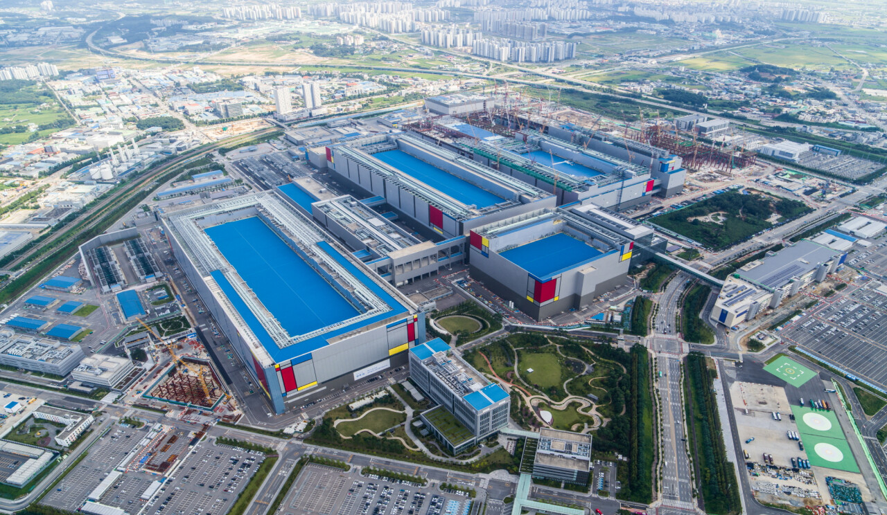
Intel to Start High-Volume EUV Production in Ireland, Intel 4 Node Enters Mass-production

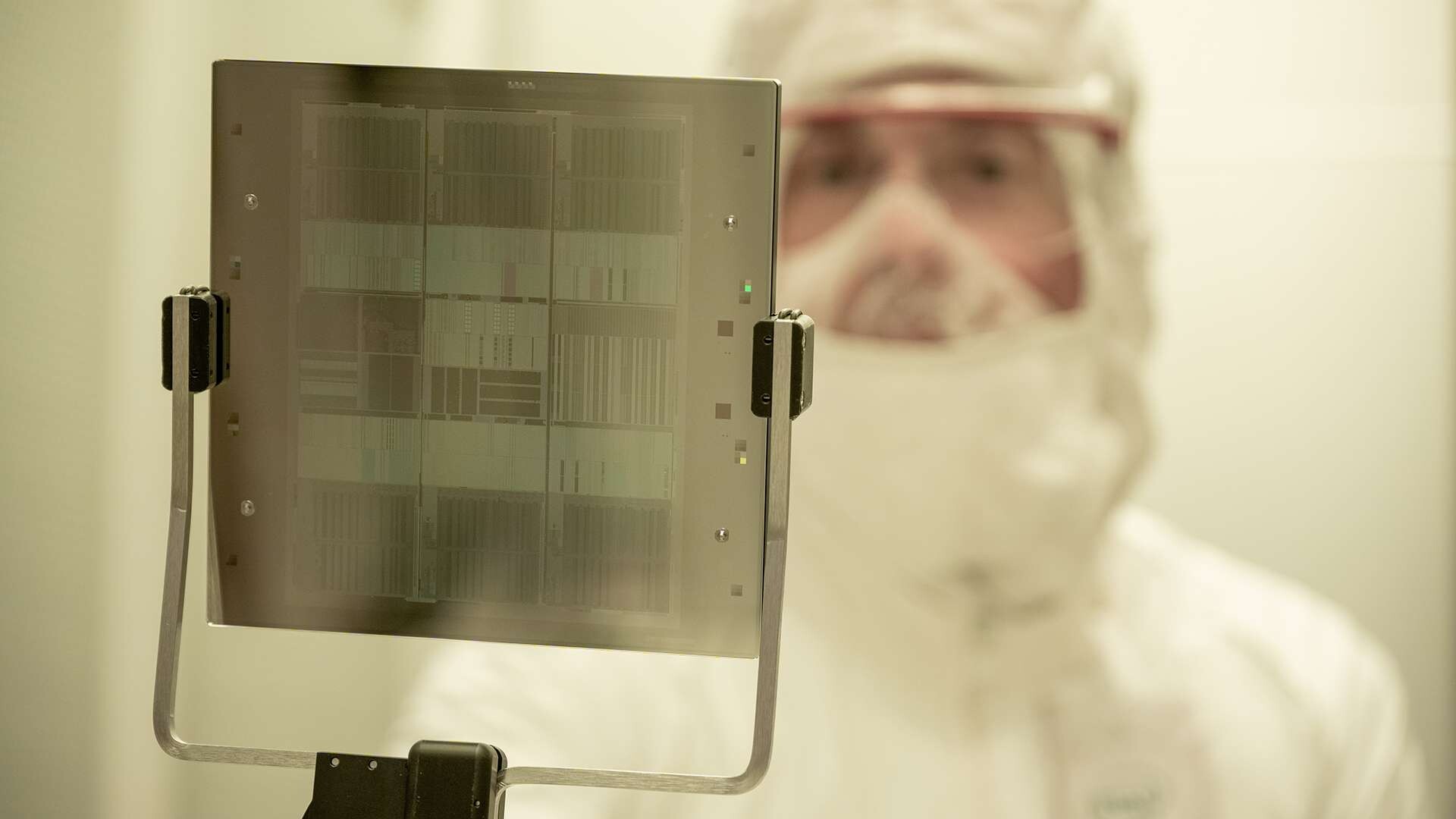
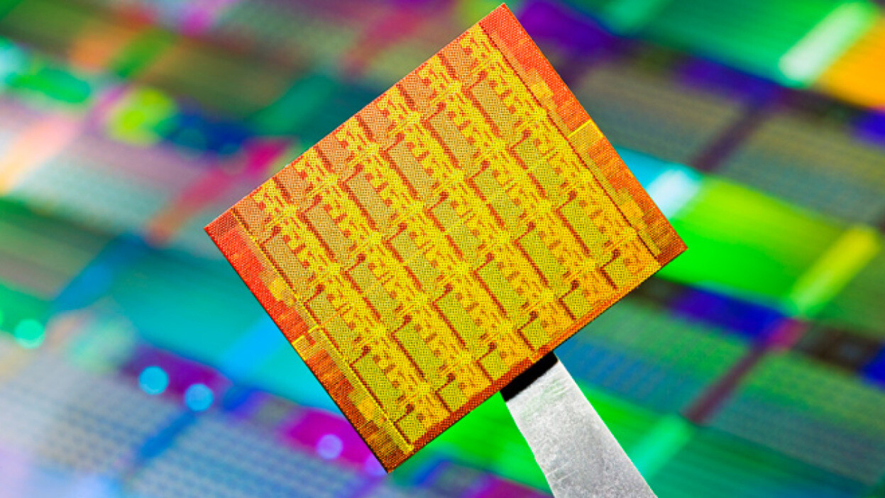
Intel Foundry Services (IFS) today announced that it will commence mass-production on its first silicon fabrication node that leverages extreme ultraviolet (EUV) lithography, Intel 4. On September 29, the Intel 4 node will start rolling at the company's facility in Leixlip, Ireland, dubbed Fab 34. CEO Pat Gelsinger, Dr. Ann Kelleher, general manager of Technology Development at Intel, and Keyvan Esfarjani, chief global operations officer, will be present at a ceremony commemorating production of the first wafers.

Intel 4 is an advanced foundry that leverages EUV, and offers both transistor densities and electrical characteristics comparable to TSMC's 5 nm-class and 4 nm-class foundry nodes. Among the first chips to be built are the compute tiles of the company's Core "Meteor Lake" processors, which contain their next-generation CPU cores. Compared to the current Intel 7 node, Intel 4 offers double the area scaling for logic libraries, a 20% iso-power improvement, and introduces the new metal-insulator-metal (MIM) capacitor.

Intel to Sell Minority Stake in IMS Nanofabrication Business to TSMC

Intel Corporation today announced that it has agreed to sell an approximately 10% stake in the IMS Nanofabrication business ("IMS") to TSMC. TSMC's investment values IMS at approximately $4.3 billion, consistent with the valuation of the recent stake sale to Bain Capital Special Situations ("Bain Capital"). Intel will retain majority ownership of IMS, which will continue to operate as a standalone subsidiary under the leadership of CEO Dr. Elmar Platzgummer. The transaction is expected to close in the fourth quarter of 2023.

IMS is the established industry leader in multi-beam mask writing tools required to develop advanced extreme ultraviolet lithography (EUV), which is broadly adopted in leading-edge technology nodes that enable the most demanding computing applications, such as artificial intelligence (AI) and mobile. Together, Bain Capital and TSMC's investments provide IMS with increased independence and reinforce confidence in the significant opportunity ahead of IMS. This added autonomy will help IMS accelerate its growth and drive the next phase of lithography technology innovation to enable the industry's transition into new patterning systems, such as high-numerical-aperture (high-NA) EUV.

Intel Reports Second-Quarter 2023 Financial Results, Foundry Services Business up

Intel Corporation today reported second-quarter 2023 financial results. "Our Q2 results exceeded the high end of our guidance as we continue to execute on our strategic priorities, including building momentum with our foundry business and delivering on our product and process roadmaps," said Pat Gelsinger, Intel CEO. "We are also well-positioned to capitalize on the significant growth across the AI continuum by championing an open ecosystem and silicon solutions that optimize performance, cost and security to democratize AI from cloud to enterprise, edge and client."

David Zinsner, Intel CFO, said, "Strong execution, including progress towards our $3 billion in cost savings in 2023, contributed to the upside in the quarter. We remain focused on operational efficiencies and our Smart Capital strategy to support sustainable growth and financial discipline as we improve our margins and cash generation and drive shareholder value." In the second quarter, the company generated $2.8 billion in cash from operations and paid dividends of $0.5 billion.

Samsung GDDR7 Memory Operates at Lower Voltage, Built on Same Node as 24 Gbps G6

Samsung on Wednesday announced mass-production of the world's first next-generation GDDR7 memory chips, and Ryan Smith from AnandTech scored a few technical details from the company. Apparently, the company's first production version of GDDR7 memory is built on the same D1z silicon foundry node as its 24 Gbps GDDR6 memory chip—the fastest GDDR6 chip in production. D1z is a 10 nm class foundry node that utilizes EUV lithography.

Smith also scored some electrical specs. The first-gen GDDR7 memory chip offers a data-rate of 32 Gbps at a DRAM voltage of 1.2 V, compared to the 1.35 V that some of the higher speed GDDR6 chips operate at. While the pJpb (pico-Joules per bit) is 7% higher than the current generation in absolute terms, for the 32 Gbps data-rate on offer, it is 20% lower compared to that of the 24 Gbps GDDR6 chip. Put simply, GDDR7 is 20% more energy efficient. Smith remarks that this energy-efficiency gain is purely architectural, and isn't a from any refinements to the D1z node. GDDR7 uses PAM3 signaling compared to the NRZ signaling of conventional GDDR6, and the PAM4 signalling of the GDDR6X non-JEDEC standard that NVIDIA co-developed with Micron Technology.

ASML reports €6.9 billion net sales and €1.9 billion net income in Q2 2023

Today ASML Holding NV (ASML) has published its 2023 second-quarter results.
  • Q2 net sales of €6.9 billion, gross margin of 51.3%, net income of €1.9 billion
  • Quarterly net bookings in Q2 of €4.5 billion of which €1.6 billion is EUV
  • ASML expects Q3 2023 net sales between €6.5 billion and €7.0 billion and a gross margin of around 50%
  • ASML expects 2023 net sales growth towards 30% compared to 2022
CEO statement and outlook
"Our second-quarter net sales came in at €6.9 billion, at the high end of our guidance, with a gross margin of 51.3%, higher than guided, primarily driven by additional DUV immersion revenue in the quarter. "Our customers across different market segments are currently more cautious due to continued macro-economic uncertainties, and therefore expect a later recovery of their markets. Also, the shape of the recovery slope is still unclear. However, our strong backlog of around €38 billion provides us with a good basis to navigate these short-term uncertainties.

ASML Issues Statement Regarding Dutch Export Control Regulations

Today the Dutch government has published the new regulations regarding export controls of semiconductor equipment. As announced earlier in March, the new export controls focus on advanced chip manufacturing technology, including the most advanced deposition and immersion lithography systems.

Due to these export control regulations, ASML will need to apply for export licenses with the Dutch government for all shipments of its most advanced immersion DUV lithography systems (TWINSCAN NXT:2000i and subsequent immersion systems). The Dutch government will determine whether to grant or deny the required export licenses and provide further details to the company on any conditions that apply.

Intel Agrees to Sell Minority Stake in IMS Nanofabrication Business to Bain Capital

Intel Corporation today announced that it has agreed to sell an approximately 20% stake in its IMS Nanofabrication GmbH ("IMS") business to Bain Capital Special Situations ("Bain Capital"), in a transaction that values IMS at approximately $4.3 billion. The transaction is expected to close in the third quarter of 2023. IMS will operate as a standalone subsidiary and will continue to be led by CEO Dr. Elmar Platzgummer.

Since inventing multi e-beam technology and introducing the first commercial multi-beam mask writer in 2015, Vienna, Austria-based IMS has been an industry leader in multi-beam mask writing for advanced technology nodes. Intel initially invested in IMS in 2009 and ultimately acquired the business in 2015. Since the acquisition, IMS has delivered a significant return on investment to Intel while growing its workforce and production capacity by four times and delivering three additional product generations.

Intel's New Chip to Advance Silicon Spin Qubit Research for Quantum Computing

Today, Intel announced the release of its newest quantum research chip, Tunnel Falls, a 12-qubit silicon chip, and it is making the chip available to the quantum research community. In addition, Intel is collaborating with the Laboratory for Physical Sciences (LPS) at the University of Maryland, College Park's Qubit Collaboratory (LQC), a national-level Quantum Information Sciences (QIS) Research Center, to advance quantum computing research.

"Tunnel Falls is Intel's most advanced silicon spin qubit chip to date and draws upon the company's decades of transistor design and manufacturing expertise. The release of the new chip is the next step in Intel's long-term strategy to build a full-stack commercial quantum computing system. While there are still fundamental questions and challenges that must be solved along the path to a fault-tolerant quantum computer, the academic community can now explore this technology and accelerate research development."—Jim Clarke, director of Quantum Hardware, Intel

AMD EPYC "Bergamo" Uses 16-core Zen 4c CCDs, Barely 10% Larger than Regular Zen 4 CCDs

A SemiAnalysis report sheds light on just how much smaller the "Zen 4c" CPU core is compared to the regular "Zen 4." AMD's upcoming high core-count enterprise processor for cloud data-center deployments, the EPYC "Bergamo," is based on the new "Zen 4c" microarchitecture. Although with the same ISA as "Zen 4," the "Zen 4c" is essentially a low-power, lite version of the core, with significantly higher performance/Watt. The core is physically smaller than a regular "Zen 4" core, which allows AMD to create CCDs (CPU core dies) with 16 cores, compared to the current "Zen 4" CCD with 8.

The 16-core "Zen 4c" CCD is built on the same 5 nm EUV foundry node as the 8-core "Zen 4" CCD, and internally features two CCX (CPU core complex), each with 8 "Zen 4c" cores. Each of the two CCX shares a 16 MB L3 cache among the cores. The SemiAnalysis report states that the dedicated L2 cache size of the "Zen 4c" core remains at 1 MB, just like that of the regular "Zen 4." Perhaps the biggest finding is their die-size estimation, which puts the 16-core "Zen 4c" CCD just 9.6% larger in die-area, than the 8-core "Zen 4" CCD. That's 72.7 mm² per CCD, compared to 66.3 mm² of the regular 8-core "Zen 4" CCD.

TSMC CFET Transistors in the Lab, Still Many Generations Away

During the European Technology Symposium 2023, TSMC presented additional details regarding the upcoming complementary FET (CFET) technology to power the next generation of silicon-based devices. With Nanosheet replacing FinFET, the CFET technology will do the same to the Gate All Around FET (GAAFET) Nanosheet nodes. As the company notes, CFET transistors are now in the TSMC labs and are being tested for performance, efficiency, and density. Compared to GAAFET, CFET will provide greater design in all of those areas, but it will require some additional manufacturing steps to get the chip working as intended. Integrating both p-type and n-type FETs into a single device, CFET will require the use of High NA EUV scanners with high precision and high power to manufacture it.

The use of CFET, as the roadmap shows, is one of the last steps in the world of silicon. It will require the integration of new materials into the manufacturing process, resulting in a greater investment into research and development that is in charge of node creation. Kevin Zhang, senior vice president at TSMC, responsible for technology roadmap and business development, notes: "Let me make a clarification on that roadmap, everything beyond the Nanosheet is something we will put on our [roadmap] to tell you there is still future out there. We will continue to work on different options. I also have the add on to the one-dimensional material-[based transistors] […], all of those are being researched on being investigated on the future potential candidates right now, we will not tell you exactly the transistor architecture will be beyond the Nanosheet."

Micron to Bring EUV Technology to Japan, Advancing Next-Generation Memory Manufacturing

Micron Technology, Inc. announced today it will be introducing extreme ultraviolet (EUV) technology to Japan, tapping this sophisticated patterning technology to manufacture its next generation of DRAM, the 1-gamma (1γ) node. Micron will be the first semiconductor company to bring EUV technology to Japan for production, with its Hiroshima fab playing a critical role in the company's development of the 1-gamma node. Micron expects to invest up to 500 billion yen in 1-gamma process technology over the next few years, with close support from the Japanese government, to enable the next wave of end-to-end technology innovation such as rapidly emerging generative artificial intelligence (AI) applications.

With each successive advancement in process technology to scale memory cells and advance performance, Micron enables increased memory density, improvement in power efficiency and lower cost per bit, helping to unlock new opportunities for digitization, sustainability and green transformation, and automation. The introduction of 1-gamma follows the development of Micron's 1-beta (1β), the industry's most advanced DRAM node today, which Micron mass produces in its Hiroshima fab. Micron continues to make progress on its EUV integration plans and expects to ramp EUV into production on the 1-gamma node in Taiwan and Japan from 2025 onwards.

Huawei Reportedly Develops Chip Design Tools for 14 nm and Above

Amid the US sanctions, Chinese technology giant Huawei has reportedly developed tools to create processors with 14 nm and above lithography. According to Chinese media Yicai, Huawei and its semiconductor partners have teamed up to create replacement tools in place of US chip toolmakers like Cadence, Synopsys, and Mentor/Siemens. These three companies control all of the world's Electronic Design Automation (EDA) tools used for every step of chip design, from architecture to placement and routing to the final physical layout. Many steps need to be taken before making a tapeout of a physical chip, and Huawei's newly developed EDA tools will help the Chinese industry with US sanctions which crippled Huawei for a long time.

Having no access to US-made chipmaking tools, Huawei has invested substantial time into making these EDA tools. However, with competing EDA makers supporting lithography way below 14 nm, Huawei's job still needs to be completed. Chinese semiconductor factories are currently capable of 7 nm chip production, and Huawei itself is working on making a sub-7 nm EUV scanner to aid manufacturing goals and compete with the latest from TSMC and other. If Huawei can create EUV scanners that can achieve transistor sizes smaller than 7 nm, we expect to see their EDA tools keep pace as well. It is only a matter of time before they announce adaptation for smaller nodes.

Intel Arc "Battlemage" to Double Shader Count, Pack Larger Caches, Use TSMC 4 nm

Intel's next-generation Arc "Battlemage" GPU is expected to numerically-double its shader counts, according to a report by RedGamingTech. The largest GPU from the Arc "Battlemage" series, the "BMG-G10," aims to power SKUs that compete in the performance segment. The chip is expected to be built on a TSMC 4 nm-class EUV node, similar to NVIDIA's GeForce "Ada" GPUs, and have a die-size similar to that of the "AD103" silicon powering the GeForce RTX 4080.

Among the juiciest bits from this report are that the top "Battlemage" chip will see its Xe Core count doubled to 64, up from 32 on the top "Alchemist" part. This would see its execution unit (EU) count doubled to 1,024, and unified shader counts at 8,192. Intel is expected to give the chip clock speeds in excess of 3.00 GHz. The Xe Cores themselves could see several updates, including IPC uplifts, and support for new math formats. The memory sub-system is expected to see an overhaul, with a large 48 MB on-die L2 cache. While the memory bus is unchanged at 256-bit wide, the memory speed could see a significant increase up from the 16-17.5 Gbps on the Arc A770. As for when customers can actually expect products, the RedGamingTech report puts launch of the Arc "Battlemage" series at no sooner than Q2-2024. The company is expected to launch refreshed "Alchemist+" GPUs in 2023.

Samsung Hires ex TSMC Executive to Improve Advanced IC Packaging

Business Korea got the scoop on Samsung hiring an ex TSMC executive by the name of Lin Jun-Cheng, who was with TSMC for almost 19 years. His role at Samsung will be as VP of Samsung's advanced packaging business, something he should be more than familiar with, as during his time at TSMC, he was part of no less than 450 patents involving chip packaging. Lin has also worked for Micron and more recently for a company called Skytech, that specialises in advanced IC packaging equipment.

Samsung has relied on third parties when it comes to more advanced chip packaging and has been behind Intel and TSMC in this area. The Business Korea article mentions that Samsung has been spending a lot of resources over the past year to build its own advanced packaging business, including hiring industry experts. Samsung has hired ex Apple, Intel and Qualcomm staff to join or head various teams related to its foundry division, not only for packaging, but also experts in various lithography processes, such as EUV. Samsung is clearly taking its foundry business seriously, even though they have had their fair share of issues with various customers over the past few years.

Intel 20A and 18A Foundry Nodes Complete Development Phase, On Track for 2024 Manufacturing

Intel Foundry Services, the in-house semiconductor foundry of Intel, announced that its 2 nm-class Intel 20A and 1.8 nm-class Intel 18A foundry nodes have completed development, and are on course for mass-producing chips on their roadmap dates. Chips are expected to begin mass-production on the Intel 20A node in the first half of 2024, while those on the Intel 18A node are expected to begin in the second half of 2024. The completion of the development phase means that Intel has finalized the specifications and performance/power targets of the nodes, the tools and software required to make the chips, and can now begin ordering them to build the nodes. Intel has been testing these nodes through 2022, and with the specs being finalized, chip-designers can accordingly wrap up development of their products to align with what these nodes have to offer.

Intel 20A (or 20-angstrom, or 2 nm) node introduces gates-all-around (GAA) RibbonFET transistors with PowerVIAs (an interconnect innovation that contributes to transistor densities). The Intel 20A node is claimed to offer a 15% performance/Watt gain over its predecessor, the Intel 3 node (FinFET EUV, 3 nm-class), which by itself offers an 18% performance/Watt gain over Intel 4 (20% perf/Watt gain over the current Intel 7 node), the node that is entering mass-production very soon. The Intel 18A node is a further refinement of Intel 20A, and introduces a design improvement to the RibbonFET that increases transistor density at scale, and a claimed 10% performance/Watt improvement over Intel 20A.

SK Hynix Enters Partner Verification Process of its 5th Gen 1β DRAM

Although DRAM is using much less refined production processes compared to the latest processors and GPUs, all the major manufacturers are continuing to shrink their manufacturing nodes step by step. Part of the reason for this, is that a node shrink doesn't have the same improvements for DRAM as it does for most types of field-effect transistors or FETs, which are mostly used for making processor logic of some kind. SK Hynix is now said to have entered the partner verification process of its 5th gen 1β DRAM, to make sure its latest 1x nm DRAM is compatible with major applications. In SK Hynix's case this should roughly translate to a 12 nm process node.

According to Chosun Media in Korea, Intel will take part in this verification, with Intel having finished verification of SK Hynix's 4th gen 1α DRAM for its 4th gen Xeon Scalable processor. Initially, SK Hynix's 5th gen 1β DRAM will be targeting server applications, so it's likely it will be tested for compatibility with the same platforms from Intel, among others. The new 1β DRAM is said to increase efficiency by more than 40 percent, although the publication didn't mention if this is power efficiency or something else. The 1β DRAM from SK Hynix, as well as Samsung—who announced its 1β DRAM in December 2022—are made using an EUV lithography process and the two Korean DRAM makers are the only two makers of DRAM that are using EUV so far.

Samsung Electronics Announces Fourth Quarter and FY 2022 Results, Profits at an 8-year Low

Samsung Electronics today reported financial results for the fourth quarter and the fiscal year 2022. The Company posted KRW 70.46 trillion in consolidated revenue and KRW 4.31 trillion in operating profit in the quarter ended December 31, 2022. For the full year, it reported 302.23 trillion in annual revenue, a record high and KRW 43.38 trillion in operating profit.

The business environment deteriorated significantly in the fourth quarter due to weak demand amid a global economic slowdown. Earnings at the Memory Business decreased sharply as prices fell and customers continued to adjust inventory. The System LSI Business also saw a decline in earnings as sales of key products were weighed down by inventory adjustments in the industry. The Foundry Business posted a new record for quarterly revenue while profit increased year-on-year on the back of advanced node capacity expansion as well as customer base and application area diversification.

Japan and the Netherlands Said to Join US in Blocking Access to Chip Making Tools for China

According to Bloomberg, Japan and the Netherlands are getting ready to join the US in limiting access to advanced semiconductor manufacturing equipment for China. The three nations are currently in talks—that might end as soon as today—over how they can impose joint limits on what kind of equipment and tools can be exported to China. Apparently there will be no official announcement if a deal is struck, instead the restrictions will simply be implemented as required.

Bloomberg states that the Netherlands will expand export restrictions that ASML is already under, which according to the publication means stricter export rules around DEUV machines, which are used in cutting edge semiconductor nodes. Japan is said to implement similar export restrictions for Nikon as well as Tokyo Electron, with the US already having implemented restrictions for Applied Materials. The export restriction deal is in part being done to appease US equipment makers, who have complained that their international competitors haven't been under the same export restrictions when it comes to China, as they have. The question is if the export restrictions will hinder China in the long run, or if the nation will simply push ahead and develop its own, competing semiconductor manufacturing tools.

Update Jan 28th: Japan and the Netherlands reached an agreement with the US on Friday and the two countries are said to be making individual announcements with regards to their individual agreements with the US.

Intel Xeon "Sapphire Rapids" to be Quickly Joined by "Emerald Rapids," "Granite Rapids," and "Sierra Forest" in the Next Two Years

Intel's server processor lineup led by the 4th Gen Xeon Scalable "Sapphire Rapids" processors face stiff competition from AMD 4th Gen EPYC "Genoa" processors that offer significantly higher multi-threaded performance per Watt on account of a higher CPU core-count. The gap is only set to widen, as AMD prepares to launch the "Bergamo" processor for cloud data-centers, with core-counts of up to 128-core/256-thread per socket. A technologically-embattled Intel is preparing quick counters as many as three new server microarchitecture launches over the next 23 months, according to Intel, in its Q4-2022 Financial Results presentation.

The 4th Gen Xeon Scalable "Sapphire Rapids," with a core-count of up to 60-core/120-thread, and various application-specific accelerators, witnessed a quiet launch earlier this month, and is shipping to Intel customers. The company says that it will be joined by the Xeon Scalable "Emerald Rapids" architecture in the second half of 2023; followed by "Granite Rapids" and "Sierra Forest" in 2024. Built on the same LGA4677 package as "Sapphire Rapids," the new "Emerald Rapids" MCM packs up to 64 "Raptor Cove" CPU cores, which support higher clock-speeds, higher memory speeds, and introduce the new Intel Trust Domain Extensions (TDX) instruction-set. The processor retains the 8-channel DDR5 memory interface, but with higher native memory speeds. The chip's main serial interface is a PCI-Express Gen 5 root-complex with 80 lanes. The processor will be built on the last foundry-level refinement of the Intel 7 node (10 nm Enhanced SuperFin); many of these refinements were introduced with the company's 13th Gen Core "Raptor Lake" client processors.

ASML Reports €21.2 Billion Net Sales and €5.6 Billion Net Income in 2022

Today ASML Holding NV (ASML) has published its 2022 fourth-quarter and full-year results. "Our fourth-quarter net sales came in around the midpoint of our guidance at €6.4 billion. The gross margin of 51.5% was above our guidance due to additional upgrades and insurance settlement for last year's ASML Berlin fire. "For ASML, 2022 was another strong year ending with total net sales for the year of €21.2 billion, gross margin of 50.5% and a record backlog at the end of 2022 of €40.4 billion.

"We continue to see uncertainty in the market caused by inflation, rising interest rates, risk of recession and geopolitical developments related to export controls. However, our customers indicate that they expect the market to rebound in the second half of the year. Considering our order lead times and the strategic nature of lithography investments, demand for our systems therefore remains strong.

AMD Ryzen 7040 Series "Phoenix Point" Mobile Processor I/O Detailed: Lacks PCIe Gen 5

The online datasheets of some of the first AMD Ryzen 7040 series "Phoenix Point" mobile processors went live, detailing the processor's I/O feature-set. We learn that AMD has decided to give PCI-Express Gen 5 a skip with this silicon, at least in its mobile avatar. The Ryzen 7040 SoC puts out a total of 20 PCI-Express Gen 4 lanes, all of which are "usable" (i.e. don't count 4 lanes toward chipset-bus). This would mean that the silicon has a full PCI-Express 4.0 x16 interface for discrete graphics, and a PCI-Express 4.0 x4 link for a CPU-attached M.2 NVMe slot; unlike the "Raphael" desktop MCM and the "Dragon Range" mobile MCM, whose client I/O dies put out a total of 28 Gen 5 lanes (24 usable, with x16 PEG + two x4 toward CPU-attached M.2 slots).

Another interesting aspect about "Phoenix Point" is its memory controllers. The SoC features a dual-channel (four sub-channel) DDR5 memory interface, besides support for LPDDR5 and LPDDR5x. DDR5-5600 and LPDDR5-7600 are the native speeds supported. What's really interesting is the maximum amount of memory supported, which stands at 256 GB—double that of "Raphael" and "Dragon Range," which top out at 128 GB. This bodes well for the eventual Socket AM5 APUs AMD will design based on the "Phoenix Point" silicon. Older Ryzen 5000G "Cezanne" desktop APUs are known for superior memory overclocking capabilities to 5000X "Vermeer," with the monolithic nature of the silicon favoring latencies. Something similar could be expected from "Phoenix Point."

Samsung Said to be Increasing Chip Production While Inflation is Increasing Cost of New Fabs

According to Reuters, Samsung is gearing up to increase the chip production capacity at its P3 factory in Pyeongtaek in South Korea, despite the fact that there's a general slowdown in the semiconductor industry, in addition to the general economic downturn. Samsung is apparently planning on adding 12-inch wafer capacity for DRAM, while also adding more 4 nm chip capacity. The P3 fab kicked off production of Samsung's most cutting-edge NAND flash chips earlier this year and is the company's largest fab overall. According to Reuters, Samsung is aiming to add at least 10 new EUV machines in 2023.

In related news via The Elec, Samsung has seen costs increase significantly when it comes to materials costs relating to the expansion of the P3 fab. So far, the company has racked up extra costs of over a trillion korean Won, or more than US$786 million, largely due to all of its contractors having raised their prices. The report also mentioned that some parts of the expansion of the P3 fab has been delayed by as much as a year, which isn't good news for Samsung and it likely means that the company will see further increases in costs before the expansions are finished.

Huawei Prepares EUV Scanner for Sub-7 nm Chinese Chips

Huawei, the Chinese technology giant, has reportedly filed patents that it is developing extreme ultraviolet (EUV) scanners for use in the manufacturing process of semiconductors. This news comes amid increasing tensions between Huawei and the US government, which has imposed a series of sanctions on the company in recent years. According to UDN, Huawei has filed a patent that covers the entire EUV scanner with a 13.5 nm EUV light source, mirrors, lithography for printing circuits, and proper system control. While filing a patent is not the same as creating an accurate EUV scanner, it could enable China to produce a class of chips below 7 nm and have a homegrown semiconductor production, despite the ever-increasing US sanctions.

The development of EUV scanners is a significant milestone for Huawei and the semiconductor industry. However, the company's progress in this area may be hindered by the US government's sanctions, which have limited Huawei's access to certain technologies and markets. It is important to note that Chinese SMIC wanted to develop EUV fabrication based on third-party EUV tools; however, those plans were scrapped as the Wassenaar agreement came into action and prohibited the sales of advanced tools to Chinese companies. Huawei's development could represent a new milestone for the entire Chinese industry.

Samsung Electronics Develops Industry's First 12nm-Class DDR5 DRAM

Samsung Electronics Co., Ltd., the world leader in advanced memory technology, today announced the development of its 16-gigabit (Gb) DDR5 DRAM built using the industry's first 12-nanometer (nm)-class process technology, as well as the completion of product evaluation for compatibility with AMD. "Our 12 nm-range DRAM will be a key enabler in driving market-wide adoption of DDR5 DRAM," said Jooyoung Lee, Executive Vice President of DRAM Product & Technology at Samsung Electronics. "With exceptional performance and power efficiency, we expect our new DRAM to serve as the foundation for more sustainable operations in areas such as next-generation computing, data centers and AI-driven systems."

"Innovation often requires close collaboration with industry partners to push the bounds of technology," said Joe Macri, Senior VP, Corporate Fellow and Client, Compute and Graphics CTO at AMD. "We are thrilled to once again collaborate with Samsung, particularly on introducing DDR5 memory products that are optimized and validated on "Zen" platforms."

AMD Explains the Economics Behind Chiplets for GPUs

AMD, in its technical presentation for the new Radeon RX 7900 series "Navi 31" GPU, gave us an elaborate explanation on why it had to take the chiplets route for high-end GPUs, devices that are far more complex than CPUs. The company also enlightened us on what sets chiplet-based packages apart from classic multi-chip modules (MCMs). An MCM is a package that consists of multiple independent devices sharing a fiberglass substrate.

An example of an MCM would be a mobile Intel Core processor, in which the CPU die and the PCH die share a substrate. Here, the CPU and the PCH are independent pieces of silicon that can otherwise exist on their own packages (as they do on the desktop platform), but have been paired together on a single substrate to minimize PCB footprint, which is precious on a mobile platform. A chiplet-based device is one where a substrate is made up of multiple dies that cannot otherwise independently exist on their own packages without an impact on inter-die bandwidth or latency. They are essentially what should have been components on a monolithic die, but disintegrated into separate dies built on different semiconductor foundry nodes, with a purely cost-driven motive.
Return to Keyword Browsing
May 21st, 2024 09:19 EDT change timezone

New Forum Posts

Popular Reviews

Controversial News Posts