News Posts matching #EUV

Return to Keyword Browsing

TSMC Ramps Up 3 nm Node Production

TSMC has had quite a good time recently. They are having all of their capacity fully booked and the development of new semiconductor nodes is going good. Today, thanks to the report of DigiTimes, we have found out that TSMC is ramping up the production lines to prepare for 3 nm high-volume manufacturing. The 3 nm node is expected to enter HVM in 2022, which is not that far away. In the beginning, the new node is going to be manufactured on 55.000 wafers of 300 mm size, and it is expected to reach as much as 100.000 wafers per month output by 2023. With the accelerated purchase of EUV machines, TSMC already has all of the equipment required for the manufacturing of the latest node. We are waiting to see more details on the 3 nm node as we approach its official release.

Samsung Foundry to Become Sole Manufacturer of Qualcomm Snapdragon 875 on 5 nm EUV Manufacturing Process

Rumors fresh of South Korean shores claim that Samsung has snagged a position as sole provider for Qualcomm's Snapdragon 875 SoC on its 5 nm EUV manufacturing process. The reason for this, according to a supposed industry insider, boiled down to money (as it almost always does): Samsung simply offered lower pricing for chips manufactured under its 5 nm EUV process than TSMC did. The deal has been claimed to be worth some $840M. This makes sense, as Samsung has a considerable product portfolio - including lucrative memory fabrication - from which it can pool resources so as to lower pricing for new manufacturing technologies, whereas TSMC can only count on revenues it brings in from contracted silicon manufacturing deals.

Samsung's 5 nm EUV will still offer the now tried-and-true FinFet transistor design - next-generation GAAFET (gate all-around FET) are reserved for the companies' 3 nm efforts. This piece of news directly contradicts Digitimes' earlier reporting on Qualcomm leaving Samsung as a foundry partner due to lower than adequate yields for Samsung's 5 nm EUV. With Samsung already manufacturing NVIDIA's Ampere on its 8 nm node, and now with a confirmed high-volume client with Qualcomm, this likely means more available capacity for other TSMC clients - of which we could mention AMD and Apple.

NVIDIA GeForce RTX 3090 and 3080 Specifications Leaked

Just ahead of the September launch, specifications of NVIDIA's upcoming RTX Ampere lineup have been leaked by industry sources over at VideoCardz. According to the website, three alleged GeForce SKUs are being launched in September - RTX 3090, RTX 3080, and RTX 3070. The new lineup features major improvements: 2nd generation ray-tracing cores and 3rd generation tensor cores made for AI and ML. When it comes to connectivity and I/O, the new cards use the PCIe 4.0 interface and have support for the latest display outputs like HDMI 2.1 and DisplayPort 1.4a.

The GeForce RTX 3090 comes with 24 GB of GDDR6X memory running on a 384-bit bus at 19.5 Gbps. This gives a memory bandwidth capacity of 936 GB/s. The card features the GA102-300 GPU with 5,248 CUDA cores running at 1695 MHz, and is rated for 350 W TGP (board power). While the Founders Edition cards will use NVIDIA's new 12-pin power connector, non-Founders Edition cards, from board partners like ASUS, MSI and Gigabyte, will be powered by two 8-pin connectors. Next up is specs for the GeForce RTX 3080, a GA102-200 based card that has 4,352 CUDA cores running at 1710 MHz, paired with 10 GB of GDDR6X memory running at 19 Gbps. The memory is connected with a 320-bit bus that achieves 760 GB/s bandwidth. The board is rated at 320 W and the card is designed to be powered by dual 8-pin connectors. And finally, there is the GeForce RTX 3070, which is built around the GA104-300 GPU with a yet unknown number of CUDA cores. We only know that it has the older non-X GDDR6 memory that runs at 16 Gbps speed on a 256-bit bus. The GPUs are supposedly manufactured on TSMC's 7 nm process, possibly the EUV variant.

TSMC Owns 50% of All EUV Machines and Has 60% of All EUV Wafer Capacity

TSMC had been working super hard in the past few years and has been investing in lots of new technologies to drive the innovation forward. At TSMC's Technology Symposium held this week was, the company has presented various things like the update on its 12 nm node, as well as future plans for node development. One of the most interesting announcements made this week was TSMC's state and ownership of Extreme Ultra-Violet (EUV) machines. ASML, the maker of these EUV machines used to etch the pattern on silicon, has been the supplier of the Taiwanese company. TSMC has announced that they own an amazing 50% of all EUV machine installations.

What is more important is the capacity that the company achieves with it. It is reported that TSMC achieves 60% of all EUV wafer capacity in the world, which is a massive achievement of what TSMC can do with the equipment. The company right now has only two nodes on EUV in high-volume manufacturing, the 7 nm+ node and 5 nm node (which is going HVM in Q4), however, that is more than any of its competitors. All of the future nodes are to be manufactured using the EUV machines and the smaller nodes require it. As far as the competitors go, only Samsung is currently making EUV silicon on the 7 nm LPP node. Intel is yet to release some products on a 7 nm node of its own, which is the first EUV node from the company.

TSMC Details 3nm N3, 5nm N5, and 3DFabric Technology

TSMC on Monday kicked off a virtual tech symposium, where it announced its new 12 nm N12e node for IoT edge devices, announced the new 3DFabric Technology, and detailed progress on its upcoming 5 nm N5 and 3 nm N3 silicon fabrication nodes. The company maintains that the N5 (5 nm) node offers the benefits of a full node uplift over its current-gen N7 (7 nm), which recently clocked 
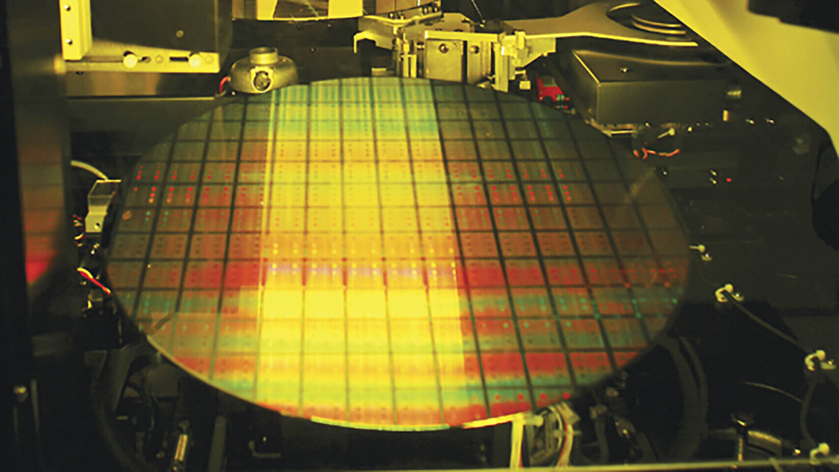
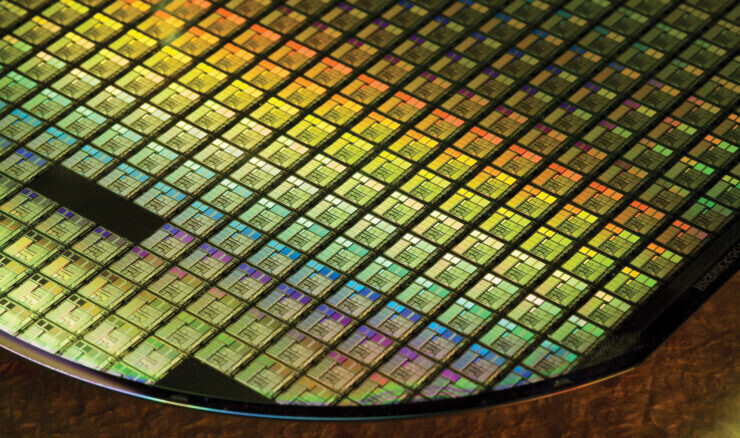
over 1 billion chips shipped. The N5 node incorporates EUV lithography more extensively than N6/N7+, and in comparison to N7 offers 30% better power at the same performance, 15% more performance at the same power, and an 80% increase in logic density. The company has commenced high-volume manufacturing on this node.

2021 will see the introduction and ramp-up of the N5P node, an enhancement of the 5 nm N5 node, offering a 10% improvement in power at the same performance, or 5% increase in performance at the same power. A nodelet of the N5 family of nodes, called N4, could see risk production in Q4 2021. The N4 node is advertised as "4 nm," although the company didn't get into its iso-power/iso-performance specifics over the N5 node. The next major node for TSMC will be the 3 nm N3 node, with massive 25%-30% improvement in power at the same performance, or 10%-15% improvement in performance at same power, compared to N5. It also offers a 70% logic density gain over N5. 3DFabric technology is a new umbrella term for TSMC's CoWoS (chip on wafer on substrate), CoW (chip on wafer), and WoW (wafer on wafer) 3-D packaging innovations, with which it plans to offer packaging innovations that compete with Intel's various new 3D chip packaging technologies on the anvil.

TSMC Ships its 1 Billionth 7nm Chip

In a bid to show off its volume production prowess and technological edge (but mostly to rub it in to rival fabs), TSMC on Thursday announced that it shipped its 1 billionth chip fabricated on its 7 nm process. If these dies were combined into one big rectangular wafer, they would cover 13 New York City blocks. TSMC's 7 nm process debuted with its N7 node, which went into volume production in April 2018, over two years ago. The fab has since mass-produced 7 nm chips for the likes of Qualcomm, Apple, and AMD, among dozens of other clients. The company now looks to monetize refinements of N7, namely the N7e and N7P (DUV refinements), while executing its crucial EUV-based N7+ node, leading up to future nodelets such as N6. Much of TSMC's growth will be propelled by 5G modems, application processors, and its pivotal role in the growth of companies such as AMD.

Samsung Announces Availability of its Silicon-Proven 3D IC Technology

Samsung Electronics Co., Ltd., a world leader in advanced semiconductor technology, today announced the immediate availability of its silicon-proven 3D IC packaging technology, eXtended-Cube (X-Cube), for today's most advanced process nodes. Leveraging Samsung's through-silicon via (TSV) technology, X-Cube enables significant leaps in speed and power efficiency to help address the rigorous performance demands of next-generation applications including 5G, artificial intelligence, high-performance computing, as well as mobile and wearable.

"Samsung's new 3D integration technology ensures reliable TSV interconnections even at the cutting-edge EUV process nodes," said Moonsoo Kang, senior vice president of Foundry Market Strategy at Samsung Electronics. "We are committed to bringing more 3D IC innovation that can push the boundaries of semiconductors."

Samsung Electronics Announces Second Quarter 2020 Results

Samsung Electronics reported today KRW 52.97 trillion in consolidated revenue and KRW 8.15 trillion in operating profit for the second quarter ended June 30, 2020. Even as the spread of COVID-19 caused closures and slowdowns at stores and production sites around the world, the Company responded to challenges through its extensive global supply chain, while minimizing the impact of the pandemic by strengthening online sales channels and optimizing costs.

Quarterly operating profit rose 26 percent from the previous quarter and 23 percent from a year earlier, thanks to firm demand for memory chips and appliances, as well as a one-off gain at its Display Panel Business. A partial recovery in global demand since May also helped offset some COVID-19 effects, resulting in higher earnings than initially expected. Revenue in the quarter fell 4 percent from the previous quarter and 6 percent from a year earlier due to reduced sales of smartphones and other devices.

Samsung's 5 nm EUV Node Struggles with Yields

Semiconductor manufacturing is a difficult process. Often when a new node is being developed, there are new materials introduced that may cause some yield issues. Or perhaps with 7 nm and below nodes, they are quite difficult to manufacture due to their size, as the transistor can get damaged by the smallest impurity in silicon. So manufacturers have to be extra careful and must spend more time on the development of new nodes. According to industry sources over at DigiTimes, we have information that Samsung is struggling with its 5 nm EUV node.

This unfortunate news comes after the industry sources of DigiTimes reported that Qualcomm's next-generation 5G chipsets could be affected if Samsung doesn't improve its yields. While there are no specific pieces of information on what is the main cause of bad yields, there could be a plethora of reasons. From anything related to manufacturing equipment to silicon impurities. We don't know yet. We hope that Samsung can sort out these issues in time, so Qualcomm wouldn't need to reserve its orders at rival foundries and port the design to a new process.

TSMC Planning a 4nm Node that goes Live in 2023

TSMC is reportedly planning a stopgap between its 5 nm-class silicon fabrication nodes, and the 3 nm-class, called N4. According to the foundry's CEO, Liu Deyin, speaking at a shareholders meeting, N4 will be a 4 nm node, and an enhancement of N5P, the company's most advanced 5 nm-class node. N4 is slated for mass-production of contracted products in 2023, and could help TSMC's customers execute their product roadmaps of the time. From the looks of it, N4 is a repeat of the N6 story: a nodelet that's an enhancement of N7+, the company's most advanced 7 nm-class node that leverages EUV lithography.

TSMC Accelerates 2 nm Semiconductor Node R&D

TSMC, the world's leading semiconductor manufacturing company, has reportedly started to accelerate research and development (R&D) of its next-generation 2 nm node. Having just recently announced that they will be starting production of a 5 nm process in Q4 of 2020, TSMC is pumping out nodes very fast and much faster compared to competition like Intel and Samsung. Having an R&D budget of almost 16 billion USD, TSMC seems to be spending the funds very wisely. The 5 nm node is going into volume production this year, and smaller nodes are already being prepared.

The 3 nm node is going into trial production in the first half of 2021, while the mass production is supposed to commence in 2022. As far as the 2 nm node, TSMC has recently purchased more expensive Extreme Ultra-Violet (EUV) lithography machines for the 2 nm node. Due to the high costs of these EUV machines, TSMC's capital spending will not be revisited this year and it should remain in the $16 billion range. As far as a timeline for 2 nm is concerned, we don't know when will TSMC start trial production as the node is still in development phases.

ASML Ships Multi-Beam Inspection Tool for 5 nm

ASML Holding NV (ASML) today announced that it has completed system integration and testing of its first-generation HMI multibeam inspection (MBI) system for 5 nm nodes and beyond. The HMI eScan1000 demonstrated successful multibeam operation, simultaneously scanning nine beams on a number of test wafers. With nine beams, the eScan1000 will increase throughput up to 600% compared to single e-beam inspection tools for targeted in-line defect inspection applications.

The new MBI system includes an electron optics system capable of creating and controlling multiple primary electron beamlets and then collecting and processing the resulting secondary electron beams, limiting beam-to-beam crosstalk to less than 2% and delivering consistent imaging quality. It also features a high-speed stage to increase the system's overall throughput and a high-speed computational architecture to process the streams of data from the multiple beamlets in real time.

Samsung Expands its Foundry Capacity with A New Production Line in Pyeongtaek

Samsung Electronics Co., Ltd., a world leader in advanced semiconductor technology, today announced plans to boost its foundry capacity at the company's new production line in Pyeongtaek, Korea, to meet growing global demand for cutting-edge extreme ultraviolet (EUV) solutions.

The new foundry line, which will focus on EUV-based 5 nanometer (nm) and below process technology, has just commenced construction this month and is expected to be in full operation in the second half of 2021. It will play a pivotal role as Samsung aims to expand the use of state-of-the-art process technologies across a myriad of current and next generation applications, including 5G, high-performance computing (HPC) and artificial intelligence (AI).

NVIDIA Underestimated AMD's Efficiency Gains from Tapping into TSMC 7nm: Report

A DigiTimes premium report, interpreted by Chiakokhua, aka Retired Engineer, chronicling NVIDIA's move to contract TSMC for 7 nm and 5 nm EUV nodes for GPU manufacturing, made a startling revelation about NVIDIA's recent foundry diversification moves. Back in July 2019, a leading Korean publication confirmed NVIDIA's decision to contract Samsung for its next-generation GPU manufacturing. This was a week before AMD announced its first new-generation 7 nm products built for the TSMC N7 node, "Navi" and "Zen 2." The DigiTimes report reveals that NVIDIA underestimated the efficiency gains AMD would yield from TSMC N7.

With NVIDIA's bonhomie with Samsung underway, and Apple transitioning to TSMC N5, AMD moved in to quickly grab 7 nm-class foundry allocation and gained prominence with the Taiwanese foundry. The report also calls out a possible strategic error on NVIDIA's part. Upon realizing the efficiency gains AMD managed, NVIDIA decided to bet on TSMC again (apparently without withdrawing from its partnership with Samsung), only to find that AMD had secured a big chunk of its nodal allocation needed to support its growth in the x86 processor and discrete GPU markets. NVIDIA has hence decided to leapfrog AMD by adapting its next-generation graphics architectures to TSMC's EUV nodes, namely the N7+ and N5. The report also speaks of NVIDIA using its Samsung foundry allocation as a bargaining chip in price negotiations with TSMC, but with limited success as TSMC established its 7 nm-class industry leadership. As it stands now, NVIDIA may manufacture its 7 nm-class and 5 nm-class GPUs on both TSMC and Samsung.

TSMC Secures Orders from NVIDIA for 7nm and 5nm Chips

TSMC has reportedly secured orders from NVIDIA for chips based on its 7 nm and 5 nm silicon fabrication nodes, sources tell DigiTimes. If true, it could confirm rumors of NVIDIA splitting its next-generation GPU manufacturing between TSMC and Samsung. The Korean semiconductor giant is commencing 5 nm EUV mass production within Q2-2020, and NVIDIA is expected to be one of its customers. NVIDIA is expected to shed light on its next-gen graphics architecture at the GTC 2020 online event held later this month. With its "Turing" architecture approaching six quarters of market presence, it's likely that the decks are being cleared for a new architecture not just in HPC/AI compute product segment, but also GeForce and Quadro consumer graphics cards. Splitting manufacturing between TSMC and Samsung would help NVIDIA disperse any yield issue arriving from either foundry's EUV node, and give it greater bargaining power with both.

DigiTimes: TSMC Kicking Off Development of 2nm Process Node

A report via DigiTimes places TSMC as having announced to its investors that exploratory studies and R&D for the development of the 2 nm process node have commenced. As today's leading semiconductor fabrication company, TSMC doesn't seem to be one resting on its laurels. Their 7 nm process and derivatives have already achieved a 30% weight on the company's semiconductor orders, and their 5 nm node (which will include EUV litography) is set to hit HVM (High Volume Manufacturing) in Q2 of this year. Apart from that, not much more is known on 2 nm.

After 5 nm, which is expected to boats of an 84-87% transistor density gain over the current 7nm node, the plans are to go 3nm, with TSMC expecting that node to hit mass production come 2022. Interestingly, TSMC is planning to still use FinFET technology for its 3 nm manufacturing node, though in a new GAAFET (gate-all-around field-effect transistor) technology. TSMC's plans to deploy FinFET in under 5nm manufacturing is something that many industry analysts and specialist thought extremely difficult to achieve, with expectations for these sub-5nm nodes to require more exotic materials and transistor designs than TSMC's apparent plans

Samsung 3 nm Volume Production Facing Delays in Wake of Coronavirus Impact

Samsung's 3 nm manufacturing has already given fruits to the company, with the South Korean giant already achieving risk production at the start of this year. The company previously projected volume production of their 3 nm process to start in early 2021. However, in a report via DigiTimes, this goal may have slipped to 2022 in wake of the coronavirus pandemic.

According to the news outlet, industry sources point this delay not to Samsung's fault in the manufacturing process, but to the entire logistics movement that has to be conducted in ramping up production of a new node. Impacts on logistics and transportation services are causing delays to deliveries of EUV and other critical production equipment, without which Samsung will be hard pressed to achieve its volume production goal. How this will ultimately affect Samsung's bottom line and revenue projections remains to be seen, but this won't do any favors to the company's high-density fabrication tech - especially if rival TSMC somehow manages to skirt these issues.

Samsung Announces Industry's First EUV DRAM with Shipment of First Million Modules

Samsung Electronics Co., Ltd., the world leader in advanced memory technology, today announced that it has successfully shipped one million of the industry's first 10 nm-class (D1x) DDR4 (Double Date Rate 4) DRAM modules based on extreme ultraviolet (EUV) technology. The new EUV-based DRAM modules have completed global customer evaluations, and will open the door to more cutting-edge EUV process nodes for use in premium PC, mobile, enterprise server and datacenter applications.

"With the production of our new EUV-based DRAM, we are demonstrating our full commitment toward providing revolutionary DRAM solutions in support of our global IT customers," said Jung-bae Lee, executive vice president of DRAM Product & Technology at Samsung Electronics. "This major advancement underscores how we will continue contributing to global IT innovation through timely development of leading-edge process technologies and next-generation memory products for the premium memory market."
Samsung EUV DDR4

TSMC to Kickstart 5 nm Volume Production in April, Production Capacity Already Fully Booked

TSMC will be doing good on their previous expectations for a H2 2020 ramp-up for high volume production (HVM) on their 5 nm manufacturing process. The new 5 nm fabrication process is an Extreme Ultraviolet lithography (EUV) one, with up to 14 layers being etchable onto the silicon wafers, as opposed to five and six, respectively, for TSMC's N7+ and N6 processes.

Volume production will start with Apple's A14 SoC, meant to be driving next-generation iPhones that should hit shelves by September this year (should the COVID-19 pandemic let it be so). Apple is using two thirds of TSMC's capacity for 5 nm as is with this SoC; it's currently unclear which client (or clients) are getting the leftover one third capacity. TSMC announced back in December that they were seeing yields upwards of 80% in 5 nm EUV fabrication, so now it's "just" a matter of monetizing the process until their 3 nm iteration comes online, expectedly, in 2022.

AMD RDNA2 Graphics Architecture Detailed, Offers +50% Perf-per-Watt over RDNA

With its 7 nm RDNA architecture that debuted in July 2019, AMD achieved a nearly 50% gain in performance/Watt over the previous "Vega" architecture. At its 2020 Financial Analyst Day event, AMD made a big disclosure: that its upcoming RDNA2 architecture will offer a similar 50% performance/Watt jump over RDNA. The new RDNA2 graphics architecture is expected to leverage 7 nm+ (7 nm EUV), which offers up to 18% transistor-density increase over 7 nm DUV, among other process-level improvements. AMD could tap into this to increase price-performance by serving up more compute units at existing price-points, running at higher clock speeds.

AMD has two key design goals with RDNA2 that helps it close the feature-set gap with NVIDIA: real-time ray-tracing, and variable-rate shading, both of which have been standardized by Microsoft under DirectX 12 DXR and VRS APIs. AMD announced that RDNA2 will feature dedicated ray-tracing hardware on die. On the software side, the hardware will leverage industry-standard DXR 1.1 API. The company is supplying RDNA2 to next-generation game console manufacturers such as Sony and Microsoft, so it's highly likely that AMD's approach to standardized ray-tracing will have more takers than NVIDIA's RTX ecosystem that tops up DXR feature-sets with its own RTX feature-set.
AMD GPU Architecture Roadmap RDNA2 RDNA3 AMD RDNA2 Efficiency Roadmap AMD RDNA2 Performance per Watt AMD RDNA2 Raytracing

AMD Announces the CDNA and CDNA2 Compute GPU Architectures

AMD at its 2020 Financial Analyst Day event unveiled its upcoming CDNA GPU-based compute accelerator architecture. CDNA will complement the company's graphics-oriented RDNA architecture. While RDNA powers the company's Radeon Pro and Radeon RX client- and enterprise graphics products, CDNA will power compute accelerators such as Radeon Instinct, etc. AMD is having to fork its graphics IP to RDNA and CDNA due to what it described as market-based product differentiation.

Data centers and HPCs using Radeon Instinct accelerators have no use for the GPU's actual graphics rendering capabilities. And so, at a silicon level, AMD is removing the raster graphics hardware, the display and multimedia engines, and other associated components that otherwise take up significant amounts of die area. In their place, AMD is adding fixed-function tensor compute hardware, similar to the tensor cores on certain NVIDIA GPUs.
AMD Datacenter GPU Roadmap CDNA CDNA2 AMD CDNA Architecture AMD Exascale Supercomputer

UNISOC Launches Next-Gen 5G SoC T7520 on 6 nm EUV Manufacturing Node

UNISOC, a leading global supplier of mobile communication and IoT chipsets, today officially launched its new-generation 5G SoC mobile platform - T7520. Using cutting-edge process technology, T7520 enables an optimized 5G experience with substantially enhanced AI computing and multimedia imaging processing capabilities while lowering power consumption.

T7520 is UNISOC's second-generation 5G smartphone platform. Built on a 6 nm EUV process technology and empowered by some of the latest design techniques, it offers substantially enhanced performance at a lower level of power consumption than ever.

Samsung Electronics Begins Mass Production at New EUV Manufacturing Line

Samsung Electronics, a world leader in advanced semiconductor technology, today announced that its new cutting-edge semiconductor fabrication line in Hwaseong, Korea, has begun mass production.

The facility, V1, is Samsung's first semiconductor production line dedicated to the extreme ultraviolet (EUV) lithography technology and produces chips using process node of 7 nanometer (nm) and below. The V1 line broke ground in February 2018, and began test wafer production in the second half of 2019. Its first products will be delivered to customers in the first quarter.

Europe Readies its First Prototype of Custom HPC Processor

European Processor Initiative (EPI) is a Europe's project to kickstart a homegrown development of custom processors tailored towards different usage models that the European Union might need. The first task of EPI is to create a custom processor for high-performance computing applications like machine learning, and the chip prototypes are already on their way. The EPI chairman of the board Jean-Marc Denis recently spoke to the Next Platform and confirmed some information regarding the processor design goals and the timeframe of launch.

Supposed to be manufactured on TSMC's 6 nm EUV (TSMC N6 EUV) technology, the EPI processor will tape-out at the end of 2020 or the beginning of 2021, and it is going to be heterogeneous. That means that on its 2.5D die, many different IPs will be present. The processor will use a custom ARM CPU, based on a "Zeus" iteration of Neoverese server core, meant for general-purpose computation tasks like running the OS. When it comes to the special-purpose chips, EPI will incorporate a chip named Titan - a RISC-V based processor that uses vector and tensor processing units to compute AI tasks. The Titan will use every new standard for AI processing, including FP32, FP64, INT8, and bfloat16. The system will use HBM memory allocated to the Titan processor, have DDR5 links for the CPU, and feature PCIe 5.0 for the inner connection.

ASML to Deliver 35 EUV Systems in 2020

In a 2019 earnings call ASML, a Dutch company that is currently the world's largest semiconductor lithography supplier has been talking about the company's records and what awaits them in the future. In its 2019 earning report, ASML was forecasting the delivery of as much as 35 EUV systems in 2020. It is not a forecast per se, but rather a known fact since factories order their equipment months before they need to use it. Having previously delivered 26 EUV systems in 2019, the plan for the coming years is to boost the EUV system shipments by as much as 40% yearly. With plans to ship between 45 and 50 EUV systems in the year 2021, AMSL sees a strong revenue gain in the coming years. What is driving the demand for these machines is the use of ever-smaller semiconductor manufacturing nodes. Even at 7 nm, there is almost a need to use EUV lithography, and as you drop in size the lithography challenge becomes real, the use of EUV becomes a necessity.
Return to Keyword Browsing
May 21st, 2024 22:19 EDT change timezone

New Forum Posts

Popular Reviews

Controversial News Posts