News Posts matching #EUV

Return to Keyword Browsing

Expect High-end Navi: AMD CEO

At a Q&A session with the tech press in Las Vegas, AMD CEO Dr Lisa Su raised hopes of a high-end graphics card based on its "Navi" family of GPUs. Responding to a specific question by Gordon Ung from PC World on whether there will be a high-end competitor in the discrete graphics space, Dr Su stated that one should expect a "high-end Navi." Dr Su states: "I know those on Reddit want a high end Navi! You should expect that we will have a high-end Navi, and that it is important to have it. The discrete graphics market, especially at the high end, is very important to us. So you should expect that we will have a high-end Navi, although I don't usually comment on unannounced products."

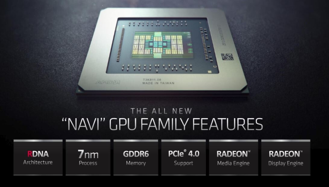
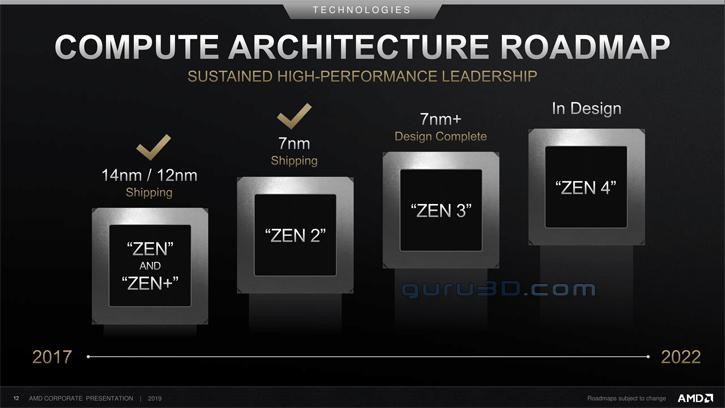
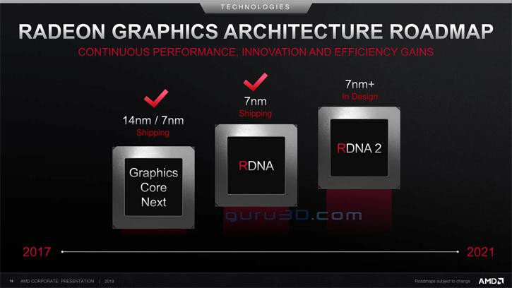
For months now, it's been speculated that AMD has been working on a larger GPU die than "Navi 10." In 2020, AMD is expected to release the "Navi 20" familly of GPUs built on 7 nm+ (EUV) node, based on the RDNA2 graphics architecture. The key design goals of RDNA2 are expected to be support for at least tier-1 variable-rate shading (VRS), and possibly hardware-accelerated ray-tracing. It's possible that "high-end Navi" belongs to this family of GPUs.

AMD to Outpace Apple as TSMC's Biggest 7nm Customer in 2020

AMD in the second half of 2020 could outpace Apple as the biggest foundry customer of TSMC for its 7 nm silicon fabrication nodes (DUV and EUV combined). There are two key factors contributing to this: AMD significantly increasing its orders for the year; and Apple transitioning to TSMC's 5 nm node for its A14 SoC, freeing up some 7 nm allocation, which AMD grabbed. AMD is currently tapping into 7 nm DUV for its "Zen 2" chiplet, "Navi 10," and "Navi 14" GPU dies. The company could continue to order 7 nm DUV until these products reach EOL; while also introducing the new "Renoir" APU die on the process. The foundry's new 7 nm+ (EUV) node will be utilized for "Zen 3" chiplets and "Navi 2#" GPU dies in 2020.

Currently, the top-5 customers for TSMC 7 nm are Apple, HiSilicon, Qualcomm, AMD, and MediaTek. Barring AMD, the others in the top-5 build mobile SoCs or 4G/5G modem chips on the node. AMD is expected to top the list as it scales up orders with TSMC. In the first half of 2020, TSMC's monthly output for 7 nm is expected to grow to 110,000 wafers per month (wpm). Apple's migration to 5 nm in 2H-2020, coupled with capacity-addition could take TSMC's 7 nm output to 140,000 wpm. AMD has reportedly booked the entire capacity-addition for 30,000 wpm, taking its allocation up to 21% in 2H-2020. Qualcomm is switching to Samsung for its next-generation SoCs and modems designed for 7 nm EUV. NVIDIA, too, is expected to built its next-gen 7 nm EUV GPUs on Samsung instead of TSMC. These moves by big players could free up significant foundry allocation at TSMC for AMD's volumes to grow in 2020.

AMD CEO To Unveil "Zen 3" Microarchitecture at CES 2020

A prominent Taiwanese newspaper reported that AMD will formally unveil its next-generation "Zen 3" CPU microarchitecture at the 2020 International CES. Company CEO Dr Lisa Su will head an address revealing three key client-segment products under the new 4th generation Ryzen processor family, and the company's 3rd generation EPYC enterprise processor family based on the "Milan" MCM that succeeds "Rome." AMD is keen on developing an HEDT version of "Milan" for the 4th generation Ryzen Threadripper family, codenamed "Genesis Peak."

The bulk of the client-segment will be addressed by two distinct developments, "Vermeer" and "Renoir." The "Vermeer" processor is a client-desktop MCM that succeeds "Matisse," and will implement "Zen 3" chiplets. "Renoir," on the other hand, is expected to be a monolithic APU that combines "Zen 2" CPU cores with an iGPU based on the "Vega" graphics architecture, with updated display- and multimedia-engines from "Navi." The common thread between "Milan," "Genesis Peak," and "Vermeer" is the "Zen 3" chiplet, which AMD will build on the new 7 nm EUV silicon fabrication process at TSMC. AMD stated that "Zen 3" will have IPC increases in line with a new microarchitecture.

AMD Ryzen 4000 Rumored to Offer Around 17% Increased Performance

AMD's upcoming Ryzen 4000 series processors will be based on the company's Zen 3 design, which will feature a deeply revised architecture aiming to offer increased performance (surprising no-one). AMD themselves have already said that Zen 3 will offer performance increases in line with the release of new architectures - and we all remember the around 15% increase achieved with the release of Zen 2 Ryzen 3000 series, which surprised even AMD on its performance capabilities. Several sources around the web are quoting an around 17% increase in performance, taking into account increased operating frequencies of Zen 3 (100 to 200 MHz at least for the enterprise solutions, which could pave the way for even higher increases in consumer-geared products) and increased IPC of its core design. The utilization of EUV in the 7 nm process shouldn't have much to do with the increased frequencies of the CPUs, and will mostly be used to reduce the number of masks that are required for production of AMD's Zen 3 CPUs (which in turn will lead to increased yields).

Sources are claiming an increase of up to 50% in Zen 3's Floating Point Units (FPU) compared to Zen 2, while integer operations should make do with a 10-12% increase. Cores should remain stable across the board - and with that increase in performance, I'd say an upper limit of 16 physical and 32 logic cores in a consumer-geared CPU is more than enough. Increased IPCs and frequencies will definitely make AMD an even better proposition for all markets - gaming in particular, where Intel still has a (slightly virtual) hold in consumer's minds.

AMD "Zen 3" Microarchitecture Could Post Significant Performance Gains

At its recent SC19 talk, AMD touched upon its upcoming "Zen 3" CPU microarchitecture. Designed for the 7 nm EUV silicon fabrication process that significantly increases transistor densities, "Zen 3" could post performance gains "right in line with what you would expect from an entirely new architecture," states AMD, referring to the roughly 15 percent IPC gains that were expected of "Zen 2" prior to its launch. "Zen 2" IPC ended up slightly over 15 percent higher than that of the original "Zen" microarchitecture. AMD's SC19 comments need not be a guidance on the IPC itself, but rather performance gains of end-products versus their predecessors.

The 7 nm EUV process, with its 20 percent transistor-density increase could give AMD designers significant headroom to increase clock speeds to meet the company's generational performance improvement targets. Another direction in which "Zen 3" could go is utilizing the additional transistor density to bolster its core components to support demanding instruction-sets such as AVX-512. The company's microarchitecture is also missing something analogous to Intel's DLBoost, an instruction-set that leverages fixed-function hardware to accelerate AI-DNN building and training. Even VIA announced an x86 microarchitecture with AI hardware and AVX-512 support. In either case, the design of "Zen 3" is complete. We'll have to wait until 2020 to find out how fast "Zen 3" is, and the route taken to get there.

TSMC Begins 3 nm Fab Construction

TSMC has been very aggressive with its approach to silicon manufacturing, with more investments into its R&D that now match or beat the capex investments of Intel. That indicates a strong demand for new technologies and TSMC's strong will not drop out of the never-ending race for more performance and smaller node sizes.

According to the sources over at DigiTimes, TSMC has acquired as much as 30 hectares of land in the Southern Taiwan Science Park to begin the construction of its fabs that are supposed to start high-volume manufacturing 3 nm node in 2023. Construction of 3 nm manufacturing facilities are set to begin in 2020 when TSMC will lay the groundwork for the new fab. The 3 nm semiconductor node is expected to be TSMC's third attempt at EUV lithography, right after the 7 nm+, and 5 nm nodes which are also based on EUV technology.

Intel Scraps 10nm for Desktop, Brazen it Out with 14nm Skylake Till 2022?

In a shocking piece of news, Intel has reportedly scrapped plans to launch its 10 nm "Ice Lake" microarchitecture on the client desktop platform. The company will confine its 10 nm microarchitectures, "Ice Lake" and "Tiger Lake" to only the mobile platform, while the desktop platform will see derivatives of "Skylake" hold Intel's fort under the year 2022! Intel gambles that with HyperThreading enabled across the board and increased clock-speeds, it can restore competitiveness with AMD's 7 nm "Zen 2" Ryzen processors with its "Comet Lake" silicon that offers core-counts of up to 10.

"Comet Lake" will be succeeded in 2021 by the 14 nm "Rocket Lake" silicon, which somehow combines a Gen12 iGPU with "Skylake" derived CPU cores, and possibly increased core-counts and clock speeds over "Comet Lake." It's only 2022 that Intel will ship out a truly new microarchitecture on the desktop platform, with "Meteor Lake." This chip will be built on Intel's swanky 7 nm EUV silicon fabrication node, and possibly integrate CPU cores more advanced than even "Willow Cove," possibly "Golden Cove."

TSMC Starts Shipping its 7nm+ Node Based on EUV Technology

TSMC today announced that its seven-nanometer plus (N7+), the industry's first commercially available Extreme Ultraviolet (EUV) lithography technology, is delivering customer products to market in high volume. The N7+ process with EUV technology is built on TSMC's successful 7 nm node and paves the way for 6 nm and more advanced technologies.

The N7+ volume production is one of the fastest on record. N7+, which began volume production in the second quarter of 2019, is matching yields similar to the original N7 process that has been in volume production for more than one year.

AMD Zen 3 Could Bid the CCX Farewell, Feature Updated SMT

With its next-generation "Zen 3" CPU microarchitecture designed for the 7 nm EUV silicon fabrication process, AMD could bid the "Zen" compute complex or CCX farewell, heralding chiplets with monolithic last-level caches (L3 caches) that are shared across all cores on the chiplet. AMD embraced a quad-core compute complex approach to building multi-core processors with "Zen." At the time, the 8-core "Zeppelin" die featured two CCX with four cores, each. With "Zen 2," AMD reduced the CPU chiplet to only containing CPU cores, L3 cache, and an Infinity Fabric interface, talking to an I/O controller die elsewhere on the processor package. This reduces the economic or technical utility in retaining the CCX topology, which limits the amount of L3 cache individual cores can access.

This and more juicy details about "Zen 3" were put out by a leaked (later deleted) technical presentation by company CTO Mark Papermaster. On the EPYC side of things, AMD's design efforts will be spearheaded by the "Milan" multi-chip module, featuring up to 64 cores spread across eight 8-core chiplets. Papermaster talked about how the individual chiplets will feature "unified" 32 MB of last-level cache, which means a deprecation of the CCX topology. He also detailed an updated SMT implementation that doubles the number of logical processors per physical core. The I/O interface of "Milan" will retain PCI-Express gen 4.0 and eight-channel DDR4 memory interface.

Moore's Law - Is it Really Dead ?

"Moore's Law" is a term coined in 1965 by Gordon Moore, who presented a paper which predicts that semiconductor scaling will allow integrated circuits to feature twice as many transistors present per same area as opposed to a chip manufactured two years ago. That means we could get same performance at half the power than the previous chip, or double the performance at same power/price in only two years time. Today we'll investigate if Moore's Law stayed true to its cause over the years and how much longer can it keep going.

TSMC to Begin Mass Production of 5nm Chips in 2020

According to industry sources over at DigiTimes, TSMC will begin mass production of its 5 nm node in March 2020, when companies using the 5 nm PDK can tape out their designs and integrate them into future products. Going into volume production two years after the 7 nm node, 5 nm is trying to put Moore's Law back on track again.

Built using the Extreme Ultra-Violet lithography (also known as EUV), 5 nm node is supposed to utilize existing FinFET transistors along with many improvements in speed, power and density when compared to existing 7 nm node. Speed is supposed to increase by around 15%, while density will improve by as much as 80%, which is excellent news for everyone. Noticeable power reduction is also present and it is now possible to have about 30% reduction in power consumption, while also enjoying additional speed and density improvements that new node brings.

AMD Readies the Low-Power "Dali" APU for Thin-and-Light Notebooks

AMD is expected to bring back its low-power APU family in 2020 with the new "Dali" silicon. Updated company roadmap slides see the inclusion of "Dali" as a "value mobile APU," positioned under "Renoir," a performance APU targeting both the mainstream notebook and desktop (socket AM4) platforms. AMD looks keen to branch out its APU business in two directions.

"Renoir" is expected to be a "Zen 2" based APU with CPU performance matching at least the Ryzen 5 3600 or 3700X, and a faster "Vega" based iGPU. It wouldn't surprise us if "Dali" is a monolithic 7 nm die with two "Zen 2" CPU cores and a tiny iGPU with 3-4 compute units. "Renoir," on the other hand, could be an MCM with an 8-core "Zen 2" chiplet and an enlarged I/O controller die that has the iGPU. "Dali" could see the light of the day only in 2020, by which time TSMC could substantially increase its 7 nm volumes and clear the decks for its new 7 nm EUV mass-production.

AMD Updates Roadmaps to Lock RDNA2 and Zen 3 onto 7nm+, with 2020 Launch Window

AMD updated its technology roadmaps to reflect a 2020 launch window for its upcoming CPU and graphics architectures, "Zen 3" and RDNA2. The two will be based on 7 nm+ , which is AMD-speak for the 7 nanometer EUV silicon fabrication process at TSMC, that promises a significant 20 percent increase in transistor-densities, giving AMD high transistor budgets and more clock-speed headroom. The roadmap slides however hint that unlike the "Zen 2" and RDNA simultaneous launch on 7th July 2019, the next-generation launches may not be simultaneous.

The slide for CPU microarchitecture states that the design phase of "Zen 3" is complete, and that the microarchitecture team has already moved on to develop "Zen 4." This means AMD is now developing products that implement "Zen 3." On the other hand, RDNA2 is still in design phase. The crude x-axis on both slides that denotes year of expected shipping, too appears to suggest that "Zen 3" based products will precede RDNA2 based ones. "Zen 3" will be AMD's first response to Intel's "Comet Lake-S" or even "Ice Lake-S," if the latter comes to fruition before Computex 2020. In the run up to RDNA2, AMD will scale up RDNA a notch larger with the "Navi 12" silicon to compete with graphics cards based on NVIDIA's "TU104" silicon. "Zen 2" will receive product stack additions in the form of a new 16-core Ryzen 9-series chip later this month, and the 3rd generation Ryzen Threadripper family.

Samsung Announces Breakthrough in Building Blocks of 3nm Circuits, Updates Roadmap

Samsung Electronics Co., Ltd., a world leader in advanced semiconductor technology, today announced its ongoing commitment to foundry innovation and service at the Samsung Foundry Forum 2019 USA, providing the silicon community with wide-ranging updates on technology advances that support the most demanding applications of today and tomorrow.

The event, held today in Santa Clara, California, features top Samsung executives and industry experts reviewing progress on semiconductor technologies and foundry platform solutions that enable developments in artificial intelligence (AI), machine learning, 5G networking, automotive, the Internet of Things (IoT), advanced data centers and many other domains.

Intel Switches Gears to 7nm Post 10nm, First Node Live in 2021

Intel's semiconductor manufacturing business has had a terrible past 5 years as it struggled to execute its 10 nanometer roadmap forcing the company's processor designers to re-hash the "Skylake" microarchitecture for 5 generations of Core processors, including the upcoming "Comet Lake." Its truly next-generation microarchitecture, codenamed "Ice Lake," which features a new CPU core design called "Sunny Cove," comes out toward the end of 2019, with desktop rollouts expected 2020. It turns out that the 10 nm process it's designed for, will have a rather short reign at Intel's fabs. Speaking at an investor's summit on Wednesday, Intel put out its silicon fabrication roadmap that sees an accelerated roll-out of Intel's own 7 nm process.

When it goes live and fit for mass production some time in 2021, Intel's 7 nm process will be a staggering 3 years behind TSMC, which fired up its 7 nm node in 2018. AMD is already mass-producing CPUs and GPUs on this node. Unlike TSMC, Intel will implement EUV (extreme ultraviolet) lithography straightaway. TSMC began 7 nm with DUV (deep ultraviolet) in 2018, and its EUV node went live in March. Samsung's 7 nm EUV node went up last October. Intel's roadmap doesn't show a leap from its current 10 nm node to 7 nm EUV, though. Intel will refine the 10 nm node to squeeze out energy-efficiency, with a refreshed 10 nm+ node that goes live some time in 2020.

TSMC Expects Most 7nm Customers to Move to 6nm Density

TSMC in its quarterly earnings call expressed confidence in that most of its 7 nm (N7) process production node customers would be looking to make the transition to their 6 nm (N6) process. In fact, the company expects that node to become the biggest target for volume ordering (and thus production) amongst its customers, since the new N6 fabrication technology will bring about a sort of "backwards compatibility" with design tools and semiconductor designs that manufacturers have already invested in for its N7 node, thus allowing for cost savings for its clients.

This is despite TSMC's N6 process being able to take advantage of extreme ultraviolet lithography (EUVL) to lower manufacturing complexity. This lowering is achieved by the fact that less exposures of the silicon are required for multi-patterning - which is needed today as TSMC's N7 uses solely deep ultraviolet (DUV) lithography. Interestingly, TSMC expects other clients to pick up its N7+ manufacturing node that aren't already using their 7nm node - the need to develop new tools and lesser design compatibility between its N7 and N7+ nodes compared no N7 and N6 being the justification. TSMC's N7+ will be the first node to leverage EUV, using up to four EUVL layers, while N6 expands it up to five layers, and the upcoming N5 cranks EUVL up to fourteen (allowing for 14 layers.)

Intel Courting Samsung to Manufacture Xe GPUs?

Intel's Xe discrete GPU project head Raja Koduri recently visited a Samsung Electronics silicon fabrication facility in Korea at the backdrop of the company's major 5 nm EUV announcement. This sparks speculation that Koduri could be exploring Samsung's portfolio of sub-10 nm contract-manufacturing offerings to mass-produce Xe discrete GPUs. Intel's own foundry business is reeling with mounting pressure from the company's main breadwinner, the client and enterprise processor businesses, to get its 10 nm node on the road. Koduri's GPU would need to leverage higher transistor densities than what Intel's 10 nm could offer, given that rival AMD is already implementing 7 nm, and NVIDIA is expected to go sub-10 nm with its future generation of GPUs.

Samsung Successfully Completes 5nm EUV Development

Samsung Electronics Co., Ltd., a world leader in advanced semiconductor technology, today announced that its 5-nanometer (nm) FinFET process technology is complete in its development and is now ready for customers' samples. By adding another cutting-edge node to its extreme ultraviolet (EUV)-based process offerings, Samsung is proving once again its leadership in the advanced foundry market.

Compared to 7 nm, Samsung's 5 nm FinFET process technology provides up to a 25 percent increase in logic area efficiency with 20 percent lower power consumption or 10 percent higher performance as a result of process improvement to enable us to have more innovative standard cell architecture. In addition to power performance area (PPA) improvements from 7 nm to 5 nm, customers can fully leverage Samsung's highly sophisticated EUV technology. Like its predecessor, 5 nm uses EUV lithography in metal layer patterning and reduces mask layers while providing better fidelity.

TSMC Completes 5 nm Design Infrastructure, Paving the Way for Silicon Advancement

TSMC announced they've completed the infrastructure design for the 5 nm process, which is the next step in silicon evolution when it comes to density and performance. TSMC's 5 nm process will leverage the company's second implementation of EUV (Extreme Ultra Violet) technology (after it's integrated in their 7 nm process first), allowing for improved yields and performance benefits.

According to TSMC, the 5 nm process will enable up to 1.8x the logic density of their 7 nm process, a 15% clock speed gain due to process improvements alone on an example Arm Cortex-A72 core, as well as SRAM and analog circuit area reduction, which means higher number of chips per wafer. The process is being geared for mobile, internet, and high performance computing applications. TSMC also provides online tools for silicon design flow scenarios that are optimized for their 5 nm process. Risk production is already ongoing.

TSMC 7nm EUV Process to Enter Mass-Production in March 2019

TSMC is giving final touches to set its flagship 7 nanometer EUV (extreme ultraviolet lithography) silicon fabrication node at its highest state of readiness for business, called mass-production. At this state, the node can mass-produce products for TSMC's customers. TSMC had taped out its first 7 nm EUV chips in October 2018. The company will also begin risk-production of the more advanced 5 nm node in April, staying on schedule. Mass production of 5 nm chips could commence in the first half of 2020.

The 7 nm EUV node augments TSMC's 7 nm DUV (deep ultraviolet lithography) node that's been already active since April 2018, and producing chips for AMD, Apple, HiSilicon, and Xilinx. At the turn of the year, 7 nm DUV made up 9 percent of TSMC's shipments. With the new node going online, 7 nm (DUV + EUV) could make up 25 percent of TSMC's output by the end of 2019.

NVIDIA to Implement 7nm EUV Node for its 2020 GPUs

NVIDIA will implement the 7 nanometer EUV (extreme ultraviolet) lithography to build its future generation of GPUs slated for 2020, according to Japanese publication MyNavi.jp. The GPU giant could be among the first customers besides IBM, to contract Samsung for 7 nm EUV mass-production of GPUs. IBM will use the Korean semiconductor giant for manufacturing Z-series processors and FPGAs. Samsung announced in October 2018 that it will begin risk-production on its 7 nm EUV node in early-2019.

An earlier report from 2018 also forecast NVIDIA implementing 7 nm DUV (deep ultraviolet) node of TSMC for its 2019 GPU lineup. With news of the company now working with Samsung on 7 nm EUV for 2020, this seems less likely. It's possible that NVIDIA could somehow split its next generation GPU lineup between TSMC 7 nm DUV and Samsung 7 nm EUV, with the latter being used for chips with higher transistor-counts, taking advantage of the node's higher deliverable transistor densities.

IBM Expands Strategic Partnership with Samsung to Include 7nm Chip Manufacturing

IBM today announced an agreement with Samsung to manufacture 7-nanometer (nm) microprocessors for IBM Power Systems , IBM Z and LinuxONE , high-performance computing (HPC) systems, and cloud offerings. The agreement combines Samsung's industry-leading semiconductor manufacturing with IBM's high-performance CPU designs. This combination is being designed to drive unmatched systems performance, including acceleration, memory and I/O bandwidth, encryption and compression speed, as well as system scaling. It positions IBM and Samsung as strategic partners leading the new era of high-performance computing specifically designed for AI.

"At IBM, our first priority is our clients," said John Acocella, Vice President of Enterprise Systems and Technology Development for IBM Systems. "IBM selected Samsung to build our next generation of microprocessors because they share our level of commitment to the performance, reliability, security, and innovation that will position our clients for continued success on the next generation of IBM hardware."

Intel Unveils a Clean-slate CPU Core Architecture Codenamed "Sunny Cove"

Intel today unveiled its first clean-slate CPU core micro-architecture since "Nehalem," codenamed "Sunny Cove." Over the past decade, the 9-odd generations of Core processors were based on incrementally refined descendants of "Nehalem," running all the way down to "Coffee Lake." Intel now wants a clean-slate core design, much like AMD "Zen" is a clean-slate compared to "Stars" or to a large extent even "Bulldozer." This allows Intel to introduce significant gains in IPC (single-thread performance) over the current generation. Intel's IPC growth curve over the past three micro-architectures has remained flat, and only grew single-digit percentages over the generations prior.

It's important to note here, that "Sunny Cove" is the codename for the core design. Intel's earlier codenaming was all-encompassing, covering not just cores, but also uncore, and entire dies. It's up to Intel's future chip-designers to design dies with many of these cores, a future-generation iGPU such as Gen11, and a next-generation uncore that probably integrates PCIe gen 4.0 and DDR5 memory. Intel details "Sunny Cove" as far as mentioning IPC gains, a new ISA (new instruction sets and hardware capabilities, including AVX-512), and improved scalability (ability to increase core-counts without running into latency problems).

Intel 7nm EUV Node Back On Track, 2x Transistor Densities Over 10nm

There could be light at the end of the tunnel for Intel's silicon fabrication business after all, as the company reported that its 7 nanometer silicon fabrication node, which incorporates EUV (extreme ultraviolet) lithography, is on track. The company stressed in its Nasdaq Investors' Conference presentation that its 7 nm EUV process is de-linked from its 10 nm DUV (deep ultraviolet) node, and that there are separate teams working on their development. The 10 nm DUV node is qualitatively online, and is manufacturing small batches of low-power mobile "Cannon Lake" Core processors.

Cannon Lake is an optical shrink of the "Skylake" architecture to the 10 nm node. Currently there's only one SKU based on it, the Core i3-8121U. Intel utilized the electrical gains from the optical shrink to redesign the client-segment architecture's FPU to support the AVX-512 instruction-set (although not as feature-rich as the company's enterprise-segment "Skylake" derivatives). The jump from 10 nm DUV to 7 nm EUV will present a leap in transistor densities, with Intel expecting nothing short of a doubling. 10 nm DUV uses a combination of 193 nm wavelength ultraviolet lasers and multi-patterning to achieve its transistor density gains over 14 nm++. The 7 nm EUV node uses an extremely advanced 135 nm indirect laser, reducing the need for multi-patterning. The same laser coupled with multi-patterning could be Intel's ticket to 5 nm.

Samsung Electronics Starts Production of EUV-based 7nm LPP Process

Samsung Electronics, a world leader in advanced semiconductor technology, today announced that it has completed all process technology development and has started wafer production of its revolutionary process node, 7LPP, the 7-nanometer (nm) LPP (Low Power Plus) with extreme ultraviolet (EUV) lithography technology. The introduction of 7LPP is a clear demonstration of Samsung Foundry's technology roadmap evolution and provides customers with a definite path to 3nm. The commercialization of its newest process node, 7LPP gives customers the ability to build a full range of exciting new products that will push the boundaries of applications such as 5G, Artificial Intelligence, Enterprise and Hyperscale Datacenter, IoT, Automotive, and Networking.

"With the introduction of its EUV process node, Samsung has led a quiet revolution in the semiconductor industry," said Charlie Bae, executive vice president of foundry sales and marketing team at Samsung Electronics. "This fundamental shift in how wafers are manufactured gives our customers the opportunity to significantly improve their products' time to market with superior throughput, reduced layers, and better yields. We're confident that 7LPP will be an optimal choice not only for mobile and HPC, but also for a wide range of cutting-edge applications."
Return to Keyword Browsing
May 21st, 2024 21:57 EDT change timezone

New Forum Posts

Popular Reviews

Controversial News Posts