News Posts matching #EUV

Return to Keyword Browsing

Annual DRAM Revenue for 2022 Expected to Reach US$91.5 Billion, with Prices Likely to Rally in 2H22, Says TrendForce

Despite the forecasted 18.6% YoY growth in total DRAM bit supply next year, the global DRAM market is still expected to shift from a shortage situation to an oversupply, according to TrendForce's latest investigations. This shift can primarily be attributed to the fact that, not only are most buyers now carrying a relatively high level of DRAM inventory, but DRAM bit demand is also expected to increase by only 17.1% YoY in 2022. On the price front, the oversupply situation will result in a drop in DRAM ASP in 2022 but not a major decline in annual DRAM revenue, thanks to the oligopolistic nature of the DRAM industry. Annual DRAM revenue for 2022 is expected to reach US$91.54 billion, which represents a slight YoY increase of 0.3%.

Based on an analysis of DRAM sufficiency ratio (which refers to the surplus of supply in comparison with demand) for each quarter in 2022, TrendForce forecasts a 15% YoY decrease in DRAM ASP for 2022, with prices undergoing the more noticeable declines during the first half of the year. Heading into 2H22, however, owing to the rise in DDR5 penetration rate, as well as the arrival of peak seasonal demand, the decline in DRAM ASP will likely narrow. TrendForce does not rule out the possibility that DRAM ASP may even hold flat or undergo an increase in 2H22.

ASML Reports €5.2 Billion Net Sales and €1.7 Billion Net Income in Q3 2021

Today, ASML Holding NV (ASML) has published its 2021 third-quarter results. "Our third-quarter net sales came in at €5.2 billion with a gross margin of 51.7%, both within our guidance. Our third-quarter net bookings came in at €6.2 billion, including €2.9 billion from EUV systems. The demand continues to be high. The ongoing digital transformation and current chip shortage fuel the need to increase our capacity to meet the current and expected future demand for Memory and for all Logic nodes. ASML expects fourth-quarter net sales between €4.9 billion and €5.2 billion with a gross margin between 51% and 52%. ASML expects R&D costs of around €670 million and SG&A costs of around €195 million. For the full year, we are on track to achieving growth approaching 35%," said ASML President and Chief Executive Officer Peter Wennink.

Samsung Starts Mass Production of Most Advanced 14 nm EUV DDR5 DRAM

Samsung Electronics, the world leader in advanced memory technology, today announced that it has begun mass producing the industry's smallest, 14-nanometer (nm), DRAM based on extreme ultraviolet (EUV) technology. Following the company's shipment of the industry-first EUV DRAM in March of last year, Samsung has increased the number of EUV layers to five to deliver today's finest, most advanced DRAM process for its DDR5 solutions.

"We have led the DRAM market for nearly three decades by pioneering key patterning technology innovations," said Jooyoung Lee, Senior Vice President and Head of DRAM Product & Technology at Samsung Electronics. "Today, Samsung is setting another technology milestone with multi-layer EUV that has enabled extreme miniaturization at 14 nm—a feat not possible with the conventional argon fluoride (ArF) process. Building on this advancement, we will continue to provide the most differentiated memory solutions by fully addressing the need for greater performance and capacity in the data-driven world of 5G, AI and the metaverse."

Samsung Confirms RDNA2-based Exynos 2200 iGPU Will Support Ray Tracing

Samsung appears to be in a hurry to beat Apple and Qualcomm at bringing real-time ray tracing to the smartphone space, with its next-generation Exynos 2200 "Pamir" SoC. The chip integrates a graphics processor based on the AMD RDNA2 architecture, codenamed "Voyager." Samsung all but confirmed that the compute units of this will feature Ray Accelerators, the hardware component that performs ray-intersection calculations. The "Voyager" iGPU, as implemented on the Exynos 2200 SoC, physically features six RDNA2 compute units (384 stream processors), and hence six Ray Accelerators.

Built on the 4 nm EUV silicon fabrication process, Exynos 2200 will feature not two, but three kinds of CPU cores—four lightweight efficiency cores, three mid-tier cores, and one ultra high-performance core. Each of these three operate in unique performance/Watt bands, giving software finer-grained control over the kinds of hardware resources they want. Samsung is expected to debut the Exynos 2200 with its next-generation Galaxy S and Galaxy Note devices.

Fabricating the Fabs: ASML Vision Document Predicts 300 Billion-Transistor Logic by 2030

"Moore's Law is alive and well," says ASML, in its vision document addressing investors. The company manufactures the machines that perform the actual task of silicon lithography—turning silicon discs into wafers of logic or storage chips. It highlighted the various technologies making progress, which will help its semiconductor-fabrication customers, such as TSMC and their hundreds of clients, sustain Moore's Law all the way through this decade. The company predicts SoCs with as many as 300 billion transistors by 2030. To achieve this, the company is innovating in two distinct directions—at the chip-level, to increase transistor density per chip to over 50 billion transistors; and at the system level, through packaging technology innovations, to reach that ultimate transistor count.

According to ASML's roadmap, at the turn of the decade, its technology enables 5 nm-class in production, and is at the cusp of a major breakthrough, nanosheet-FETs. which pave the way for 3 nm and 2 nm nodes, backed by EUV lithography. The journey from 2 nm to 1.5 nm will require another breakthrough, forked-nanosheets, and from 1.5 nm to 1 nm yet another breakthrough, CFET. Sub-1 nm fabrication will be possible toward the turn of this decade, thanks to 2D atomic channel technology, which is how chip-designers will be able to cram over 50 billion transistors per chip, and build MCM systems with over 300 billion transistors. The presentation predicts that besides 3D packaging, stacked silicon will also play a role, with multiple stacked logic layers, heterogenous chips with logic, storage, and I/O layers, stacked DRAM (up from single-digit layers to double-digits; and for NAND flash to grow from the current 176-layer, to nearly 500-layer by 2030.

Samsung Receives its First Global Carbon Footprint Certification for Logic Chips

Samsung Electronics Co., Ltd., a world leader in advanced semiconductor technology, today announced that four of its System LSI products received product carbon footprint label certification from the Carbon Trust, the first of Samsung's logic chips to do so. Having received the semiconductor industry's first carbon footprint accreditation for memory chips from the Carbon Trust in 2019, Samsung has now broadened its ESG (Environmental, Social, and Governance) spectrum with this global recognition of 'eco-friendly' logic chips. Samsung also grabbed the industry's first triple Carbon Trust Standard for Carbon, Water and Waste in June 2021.

The Carbon Trust is an independent and expert partner of organizations around the world that advises businesses on their opportunities in a sustainable, low carbon world. The Carbon Trust also measures and certifies the environmental footprint of organizations, supply chains and products. Of the various certification categories of the Carbon Trust, Samsung's System LSI products received the CO2 Measured product carbon footprint label. The label certifies the chip's carbon footprint, which informs consumers of the impact that the product and its manufacturing process have on the environment. Receiving the CO₂ Measured label is a critical first step for carbon reduction, since it verifies the current carbon emissions of the product with globally recognized specifications (PAS 2050), which Samsung can use as a benchmark to measure future carbon reductions.

IBM Unveils On-Chip Accelerated Artificial Intelligence Processor

At the annual Hot Chips conference, IBM (NYSE: IBM) today unveiled details of the upcoming new IBM Telum Processor, designed to bring deep learning inference to enterprise workloads to help address fraud in real-time. Telum is IBM's first processor that contains on-chip acceleration for AI inferencing while a transaction is taking place. Three years in development, the breakthrough of this new on-chip hardware acceleration is designed to help customers achieve business insights at scale across banking, finance, trading, insurance applications and customer interactions. A Telum-based system is planned for the first half of 2022.

Today, businesses typically apply detection techniques to catch fraud after it occurs, a process that can be time consuming and compute-intensive due to the limitations of today's technology, particularly when fraud analysis and detection is conducted far away from mission critical transactions and data. Due to latency requirements, complex fraud detection often cannot be completed in real-time - meaning a bad actor could have already successfully purchased goods with a stolen credit card before the retailer is aware fraud has taken place.

Intel Beats AMD to 6nm GPUs, Arc "Alchemist" Built on TSMC N6 Process

In its 2021 Architecture Day presentation, Intel revealed that its first performance gaming GPU, the Arc "Alchemist," is built on the TSMC N6 silicon fabrication node (6 nm). A more advanced node than the N7 (7 nm) used by AMD for its current RDNA2 GPUs, TSMC N6 leverages EUV (extreme ultraviolet) lithography, and offers 18% higher transistor density, besides power improvements. "With N6, TSMC provides an optimal balance of performance, density, and power-efficiency that are ideal for modern GPUs," said Dr Kevin Zhang, SVP of Business Development at TSMC.

With working prototypes of "Alchemist" already internally circulating as the "DG2," Intel has beaten AMD to 6 nm. Team Red is reportedly planning optical-shrinks of its RDNA2-based "Navi 22" and "Navi 23" chips to TSMC N6, and assigning them mid-range SKUs in the Radeon RX 7000 series. The company will build two higher-segment RDNA3 GPUs on the more advanced TSMC N5 (5 nm) process, which will release in 2022, and power successors to the RX 6700 series and RX 6800/6900 series.

Samsung Introduces the Industry's First 5nm Processor Powering the Next Generation of Wearables

Samsung Electronics Co., Ltd., a world leader in advanced semiconductor technology, today announced its new wearable processor, the Exynos W920. The new processor integrates an LTE modem and is the first in the industry to be built with an advanced 5-nanometer (nm) extreme ultra-violet (EUV) process node, offering powerful yet efficient performance demanded by next-generation wearable devices.

"Wearables like smartwatches are no longer just a cool gadget to have. They're now a growing part of our lifestyles to keep you fit, safe and alert," said Harry Cho, vice president of System LSI marketing at Samsung Electronics. "With the Exynos W920, future wearables will be able to run applications with visually appealing user interfaces and more responsive user experiences while keeping you connected on the go with fast LTE."

Samsung Electronics Announces Second Quarter 2021 Results

Samsung Electronics today reported financial results for the second quarter ended June 30, 2021. Total consolidated revenue was KRW 63.67 trillion, a 20% increase from the previous year and a record for the second quarter. Operating profit increased 34% from the previous quarter to KRW 12.57 trillion as market conditions improved in the memory market, operations normalized at the Austin foundry fab, and as effective global supply chain management (SCM) helped maintain solid profitability for the finished product businesses.

The Semiconductor business saw a significant improvement in earnings as memory shipments exceeded previous guidance and price increases were higher than expected, while the Company strengthened its cost competitiveness. For the Display Panel Business, a one-off gain and an increase in overall prices boosted profits.

Intel Accelerates Packaging and Process Innovations

Intel Corporation today revealed one of the most detailed process and packaging technology roadmaps the company has ever provided, showcasing a series of foundational innovations that will power products through 2025 and beyond. In addition to announcing RibbonFET, its first new transistor architecture in more than a decade, and PowerVia, an industry-first new backside power delivery method, the company highlighted its planned swift adoption of next-generation extreme ultraviolet lithography (EUV), referred to as High Numerical Aperture (High NA) EUV. Intel is positioned to receive the first High NA EUV production tool in the industry.

"Building on Intel's unquestioned leadership in advanced packaging, we are accelerating our innovation roadmap to ensure we are on a clear path to process performance leadership by 2025," Intel CEO Pat Gelsinger said during the global "Intel Accelerated" webcast. "We are leveraging our unparalleled pipeline of innovation to deliver technology advances from the transistor up to the system level. Until the periodic table is exhausted, we will be relentless in our pursuit of Moore's Law and our path to innovate with the magic of silicon."

SK hynix Reports Second Quarter 2021 Results

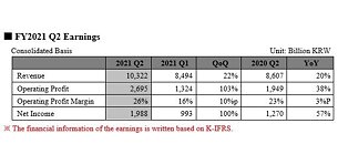
SK hynix Inc. today announced financial results for its second quarter 2021 ended on June 30, 2021. The consolidated revenue of the second quarter 2021 was 10.322 trillion won, while the operating profit amounted to 2.695 trillion won and the net income 1.988 trillion won. Operating margin for the quarter was 26% and net margin was 19%.

It was the first time in three years that SK hynix recorded the quarterly revenue of more than 10 trillion won as the memory market condition, which began to recover earlier this year, continued to improve in the second quarter. The company last logged more than 10 trillion won in the third quarter of 2018 when the memory market was booming.

SK hynix Starts Mass Production of 1anm DRAM Using EUV Equipment

SK hynix announced that it has started this month mass production of the 8 Gigabit (Gb) LPDDR4 mobile DRAM based on the 1anm, which is the fourth generation of the 10 nm process technology. As the semiconductor industry classifies the 10 nm DRAM products, naming them after the alphabets, the 1a technology is the fourth generation, following the first three generations of the 1x, 1y, and 1z. SK hynix plans to provide the latest mobile DRAM products to smartphone manufacturers from the second half of 2021. This is the first time that SK hynix adopted the EUV equipment for mass production after proving the stability of the cutting edge lithography technology through partial adoption for its 1ynm DRAM production.

As technology migration continues to ultra-micro levels, an increasing number of semiconductor companies are adopting the EUV equipment for the photo process where circuit patterns are drawn on the wafer surfaces. Industry experts believe that a semiconductor company's leadership in technology will depend on how it can fully take advantage of the EUV equipment. SK hynix plans to use the EUV technology for production of all its 1anm DRAM products going forward as it has proved the stability of the process.

Samsung 5 nm Node Struggles With Yields, Reports Indicate Less Than 50% Yielding

Semiconductor manufacturing is no easy task. Every company in that business knows that, and the hardships of silicon manufacturing have been felt by even the greatest players like Samsung and Intel. Today, according to the latest report from Business Korea, Samsung is again in trouble with its 5 nm node. It has been reported previously that Samsung is struggling with yields of its 5 nm node, however, we didn't know just how much until now. According to the sources over at Business Korea, Samsung's 5 nm semiconductor node is experiencing less than 50% yields. That means, for example, that out of 100 chips manufactured on a single silicon wafer, only half are functional. And that is not good at all.

Usually, for a node to go into high-volume manufacturing (HVM), the yielding rate needs to be around 95%. In case it is not at that level, manufacturing of that node is not very efficient and not very profitable. The V1 Line in Hwaseong, where this Samsung 5 nm is made, uses EUV tools to manufacture the new node. While the yields are currently below 50%, it is expected to improve as Samsung engineers tweak and tune the node and the tools that are running the facility. We can expect to hear more about the yields of this node in the coming months.

Samsung 3 nm GAAFET Node Delayed to 2024

Samsung's ambitious 3 nm silicon fabrication node that leverages the Gate All Around FET transistors, has reportedly been delayed to 2024. The company brands this specific node as 3GAE. 2024 is the earliest date when Samsung will be able to mass-produce chips on 3GAE, which means the company, along with Intel, will begin to fall significantly behind TSMC on foundry technology. The Taiwanese semiconductor fabrication giant will target 2 nm-class nodes around 2024, which leverages EUV multi-patterning, extensive use of cobalt in contacts and interconnects, germanium doped channels, and other in-house innovations. With Intel's foundry technology development slowing to a crawl in the sub-10 nm domain, Samsung is the only viable alternative to TSMC for cutting-edge logic chip manufacturing.

Samsung to Build a 5nm EUV Semiconductor Fab in Austin TX

Samsung Electronics plans to build a new cutting-edge semiconductor fab in Austin, Texas, according to an ETimes report. An official announcement to this effect will be made later today, when South Korean President Moon and U.S. President Biden are scheduled to hold their first Summit meeting, in Washington DC. The facility will offer third-party contract manufacturing of semiconductor chips on the 5 nanometer EUV process. Samsung has earmarked an investment of $18 billion toward the construction of this fab, which will be located close to the company's existing foundry in Texas, which manufactures chips on the 14 nm node. Samsung's investment is in response to rising demand of high-volume logic chips by major American firms such as Amazon, Google, Microsoft, and Tesla.

SK hynix Inc. Reports First Quarter 2021 Results

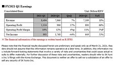
SK hynix Inc. today announced financial results for its first quarter 2021 ended on March 31, 2021. The consolidated revenue of the first quarter 2021 was 8.494 trillion won while the operating profit amounted to 1.324 trillion won, and the net income 993 billion won. Operating margin for the quarter was 16% and net margin was 12%.

The Company made better results both QoQ and YoY in the first quarter as the semiconductor market conditions improved earlier this year. Although the first quarter is usually off-season of the semiconductor industry, the Company said that the market conditions improved as demand for memory products for PCs and mobiles increased. In addition, cost competitiveness has increased as yields of major products have improved. Through this, the revenue and the operating profit increased by 7% and 37%, respectively, compared to the previous quarter.

SK Hynix Envisions the Future: 600-Layer 3D NAND and EUV-made DRAM

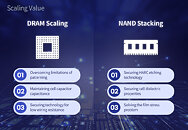
On March 22nd, the CEO of SK Hynix, Seok-Hee Lee, gave a keynote speech to the IEEE International Reliability Physics Symposium (IRPS) and shared with experts a part of its plan for the future of SK Hynix products. The CEO took the stage and delivered some conceptual technologies that the company is working on right now. At the center of the show, two distinct products stood out - 3D NAND and DRAM. So far, the company has believed that its 3D NAND scaling was very limited and that it can push up to 500 layers sometime in the future before the limit is reached. However, according to the latest research, SK Hynix will be able to produce 600-layer 3D NAND technology in the distant future.

So far, the company has managed to manufacture and sample 512Gb 176-layer 3D NAND chips, so the 600-layer solutions are still far away. Nonetheless, it is a possibility that we are looking at. Before we reach that layer number, there are various problems needed to be solved so the technology can work. According to SK Hynix, "the company introduced the atomic layer deposition (ALD) technology to further improve the cell property of efficiently storing electric charges and exporting them when needed, while developing technology to maintain uniform electric charges over a certain amount through the innovation of dielectric materials. In addition to this, to solve film stress issues, the mechanical stress levels of films is controlled and the cell oxide-nitride (ON) material is being optimized. To deal with the interference phenomenon between cells and charge loss that occur when more cells are stacked at a limited height, SK Hynix developed the isolated-charge trap nitride (isolated-CTN) structure to enhance reliability."

ASML Finishes Development of EUV Pellicles for Greater Sub-7nm Yields

ASML has finally finished development of EUV (Extreme Ultra Violet) pellicles to be employed in manufacturing processes that use the most energetic frequency of visible light to etch semiconductors onto wafers. Pellicles have been used for decades in the industry, and they are basically ultra-thin membranes that protect photomasks during the etching process - impeding particles from depositing in the substrate, which could lead to defects at the wafer level for every subsequent patterning that is laid on top of the impurity. Manufacturers such as TSMC have deployed EUV-powered manufacturing processes, but they have had to toil with potentially lower yields and increased costs with wafer analysis so as to reduce chances of defects appearing.

It's been a long time coming for EUV-capable pellicles, because these have different requirements compared to their traditional, non-EUV counterparts. However, once they are available on the market, it's expected that all semiconductor manufacturers with bleeding-edge manufacturing processes integrate them into their production flows. These will allow for better yields, which in turn should reduce overall pricing for the manufacturing processes. As an example, these EUV masks could be deployed on TSMC's 7 nm, 6 nm, 5 nm, and so on and so on. Other players other than ASML are also finishing their pellicle design, so the industry will have multiple options to integrate into their processes.

SiPearl to Manufacture its 72-Core Rhea HPC SoC at TSMC Facilities

SiPearl has this week announced their collaboration with Open-Silicon Research, the India-based entity of OpenFive, to produce the next-generation SoC designed for HPC purposes. SiPearl is a part of the European Processor Initiative (EPI) team and is responsible for designing the SoC itself that is supposed to be a base for the European exascale supercomputer. In the partnership with Open-Silicon Research, SiPearl expects to get a service that will integrate all the IP blocks and help with the tape out of the chip once it is done. There is a deadline set for the year 2023, however, both companies expect the chip to get shipped by Q4 of 2022.
When it comes to details of the SoC, it is called Rhea and it will be a 72-core Arm ISA based processor with Neoverse Zeus cores interconnected by a mesh. There are going to be 68 mesh network L3 cache slices in between all of the cores. All of that will be manufactured using TSMC's 6 nm extreme ultraviolet lithography (EUV) technology for silicon manufacturing. The Rhea SoC design will utilize 2.5D packaging with many IP blocks stitched together and HBM2E memory present on the die. It is unknown exactly what configuration of HBM2E is going to be present. The system will also see support for DDR5 memory and thus enable two-level system memory by combining HBM and DDR. We are excited to see how the final product looks like and now we wait for more updates on the project.

Samsung to Build $17 Billion Silicon Manufacturing Plant in the US by 2023

Samsung has been one of the world's biggest foundries and one of three big players still left in the leading-edge semiconductor process development and manufacturing. However, the Korean giant is always seeking ways to improve its offerings, especially for Western customers. Today, it is reported that Samsung has reportedly talked with regulators in Texas, New York, and Arizona about building a $17 billion silicon manufacturing facility in the United States. The supposed factory is going to be located near Austin, Texas, and is supposed to offer around 1800 jobs. If the deal is approved and Samsung manages to complete the project on time, the factory is supposed to start mass production in Q4 of 2023.

What process is Samsung going to manufacture in the new fab? Well, current speculations are pointing out to the 3 nm node, with Samsung's special GAAFET (Gate All Around FET) technology tied to the new node. The fab is also expected to make use of extreme ultraviolet (EUV) lithography for manufacturing. Samsung already has a facility in the US called S2, however, that will not be upgraded as it is still serving a lot of clients. Instead, the company will build new facilities to accommodate the demand for newer nodes. It is important to note that Samsung will not do any R&D work in the new fab, and the company will only manufacture the silicon there.

SK hynix Announces the Completion of M16 Plant Construction

SK hynix Inc. held a completion ceremony for its new fabrication plant M16 at headquarter located in Icheon, Gyeonggi-do, South Korea. Under the theme of "We Do Technology: Opening the Happiness", the ceremony was held as SK Group's internal event in order to adhere to the COVID-19 containment measures.

A total of 16 personnel including SK Group Chairman Chey Tae-Won and SK Group Senior Vice Chairman Chey JaeWon, SK SUPEX Council Chairman Cho DaeSik, SK hynix Vice Chairman Park Jung-ho, SK Holdings President & CEO Jang DongHyun, SK hynix CEO Seok-Hee Lee, and SK hynix Lead Independent Director Ha Yung Ku attended the on-site ceremony, along other employees and partner companies' members joined through live video conference.

TSMC Increases Orders of EUV Tools Amid High Demand

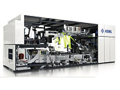
In the latest report by DigiTimes, it is said that TSMC has placed an order on 13 Extreme Ultra-Violet (EUV) machines from the Dutch company ASML. Thanks to the rapid increase in demand for its silicon, TSMC has developed plans for expansion across the next few years to satisfy the existing and upcoming customers. Usually, the company knows and can predict its demand for a future period. That is why TSMC is expanding its capacities with 13 additional ASML Twinscan NXE EUV scanners. These machines are set to be delivered by the course of 2021. It is unknown exactly when these machines are going to be delivered and installed at TSMC's facilities, however, it is fascinating that the demand for the company's capacities is ever-expanding. The price of single EUV machinery is as much as $175.75 million, so it is estimated that the expansion of capacity will cost TSMC a whopping $2.284,75 million. Despite the high pricing, the Return on Investment (ROI) is very high for TSMC.

Samsung's 5 nm Node in Production, First SoCs to Arrive Soon

During its Q3 earnings call, Samsung Electronics has provided everyone with an update on its foundry and node production development. In the past year or so, Samsung's foundry has been a producer of a 7 nm LPP (Low Power Performance) node as its smallest node. That is now changed as Samsung has started the production of the 5 nm LPE (Low Power Early) semiconductor manufacturing node. In the past, we have reported that the company struggled with yields of its 5 nm process, however, that seems to be ironed out and now the node is in full production. To contribute to the statement that the new node is doing well, we also recently reported that Samsung will be the sole manufacturer of Qualcomm Snapdragon 875 5G SoC.

The new 5 nm semiconductor node is a marginal improvement over the past 7 nm node. It features a 10% performance improvement that is taking the same power and chip complexity or a 20% power reduction of the same processor clocks and design. When it comes to density, the company advertises the node with x1.33 times increase in transistor density compared to the previous node. The 5LPE node is manufactured using the Extreme Ultra-Violet (EUV) methodology and its FinFET transistors feature new characteristics like Smart Difusion Break isolation, flexible contact placement, and single-fin devices for low power applications. The node is design-rule compatible with the previous 7 nm LPP node, so the existing IP can be used and manufactured on this new process. That means that this is not a brand new process but rather an enhancement. First products are set to arrive with the next generation of smartphone SoCs, like the aforementioned Qualcomm Snapdragon 875.

Intel's 10 nm-Geared Fab 42 Enters Operational Status

Intel has finally sounded the "full steam ahead" whistle for its Fab 42, set in Arizona. Fab 42 has a storied past to it, as Intel started its construction back in 2011. It was actually finished by 2013, and by 2014 all essential infrastructure for semiconductor fabrication was there - except for the fabrication equipment itself. You see, Intel aimed for this factory to produce 450 mm wafers (instead of the industry standard 300 mm) in the 14 nm process. However, back in 2014, Intel wasn't sure about demand for its 14 nm products - and the company was actually planning to debut 10 nm back in 2016, so it sort of made sense. Of course, then came the 10 nm delays, the 14 nm supply issues, and backporting of certain products to other less cutting-edge processes. If only Intel had had a crystal ball.
Return to Keyword Browsing
May 21st, 2024 16:10 EDT change timezone

New Forum Posts

Popular Reviews

Controversial News Posts