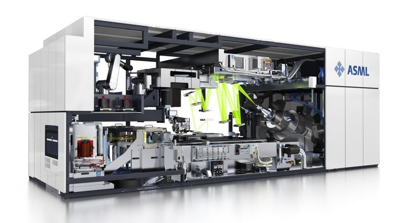
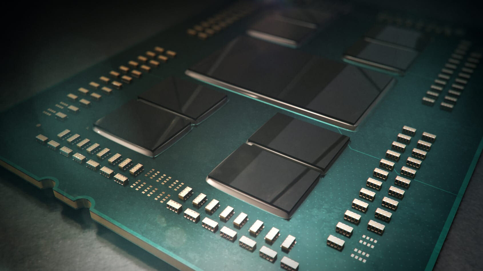
TSMC Ships its 1 Billionth 7nm Chip
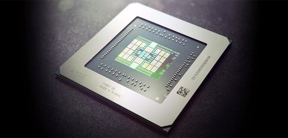
In a bid to show off its volume production prowess and technological edge (but mostly to rub it in to rival fabs), TSMC on Thursday announced that it shipped its 1 billionth chip fabricated on its 7 nm process. If these dies were combined into one big rectangular wafer, they would cover 13 New York City blocks. TSMC's 7 nm process debuted with its N7 node, which went into volume production in April 2018, over two years ago. The fab has since mass-produced 7 nm chips for the likes of Qualcomm, Apple, and AMD, among dozens of other clients. The company now looks to monetize refinements of N7, namely the N7e and N7P (DUV refinements), while executing its crucial EUV-based N7+ node, leading up to future nodelets such as N6. Much of TSMC's growth will be propelled by 5G modems, application processors, and its pivotal role in the growth of companies such as AMD.