News Posts matching #EUV

Return to Keyword Browsing

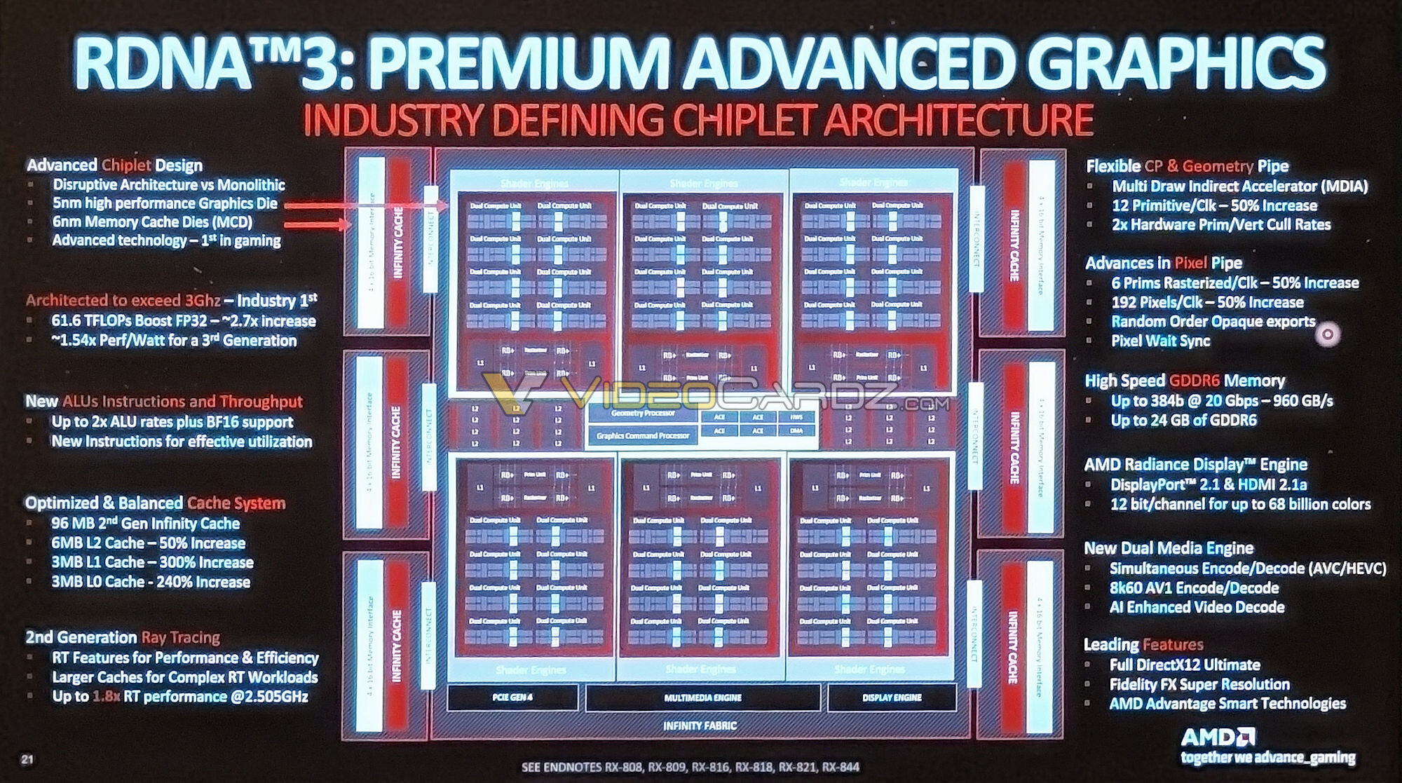
AMD RDNA3 Navi 31 GPU Block Diagram Leaked, Confirmed to be PCIe Gen 4

An alleged leaked company slide details AMD's upcoming 5 nm "Navi 31" GPU powering the next-generation Radeon RX 7900 XTX and RX 7900 XT graphics cards. The slide details the "Navi 31" MCM, with its central graphics compute die (GCD) chiplet that's built on the 5 nm EUV silicon fabrication process, surrounded by six memory cache dies (MCDs), each built on the 6 nm process. The GCD interfaces with the system over a PCI-Express 4.0 x16 host interface. It features the latest-generation multimedia engine with dual-stream encoders; and the new Radiance display engine with DisplayPort 2.1 and HDMI 2.1a support. Custom interconnects tie it with the six MCDs.

Each MCD has 16 MB of Infinity Cache (L3 cache); and a 64-bit GDDR6 memory interface (two 32-bit GDDR6 paths). Six of these add up to the GPU's 384-bit GDDR6 memory interface. In the scheme of things, the GPU has a contiguous and monolithic 384-bit wide memory bus, because every modern GPU uses multiple on-die memory controllers to achieve a wide memory bus. "Navi 31" hence has a total Infinity Cache size of 96 MB—which may be less in comparison to the 128 MB on "Navi 21," but AMD has shored up cache sizes across the GPU. The L0 caches on the compute units is now increased numerically by 240%. The L1 caches by 300%, and the L2 cache shared among the shader engines, by 50%. The RX 7900 XTX is confirmed to use 20 Gbps GDDR6 memory in this slide, for 960 GB/s of memory bandwidth.

AMD Navi 31 RDNA3 GPU Pictured

Here's the first picture of the "Navi 31" GPU at the heart of AMD's fastest next-generation graphics cards. Based on the RDNA3 graphics architecture, this will mark an ambitious attempt by AMD to build the first multi-chip module (MCM) client GPU featuring more than one logic die. MCM GPUs aren't new in the enterprise space with Intel's "Ponte Vecchio," but this would be the first such GPU meant for hardcore gaming graphics products. AMD had made MCM GPUs in the past, but those have been packages with just one logic die, surrounded by memory stacks. "Navi 31" is an MCM of as many as eight logic dies, and no memory stacks (no, those aren't HBM stacks in the picture below).

It's rumored that "Navi 31" features one or two SIMD chiplets dubbed GCDs, featuring the GPU's main number crunching machinery, the RDNA3 compute units. These chiplets are likely built on the most advanced silicon fabrication node, likely TSMC 5 nm EUV, but we'll see. The GDDR6 memory controllers handling the chip's 384-bit wide GDDR6 memory interface, will be located on separate chiplets built on a slightly older node, such as TSMC 6 nm. This is not multi-GPU-a-stick, because both SIMD chiplets have uniform access to the entire 384-bit wide memory bus (which is not 2x 192-bit but 1x 384-bit), besides the other ancillaries. The "Navi 31" MCM are expected to be surrounded by JEDEC-standard 20 Gbps GDDR6 memory chips.

Intel Hits Key Milestone in Quantum Chip Production Research

The Intel Labs and Components Research organizations have demonstrated the industry's highest reported yield and uniformity to date of silicon spin qubit devices developed at Intel's transistor research and development facility, Gordon Moore Park at Ronler Acres in Hillsboro, Oregon. This achievement represents a major milestone for scaling and working towards fabricating quantum chips on Intel's transistor manufacturing processes.

The research was conducted using Intel's second-generation silicon spin test chip. Through testing the devices using the Intel cryoprober, a quantum dot testing device that operates at cryogenic temperatures (1.7 Kelvin or -271.45 degrees Celsius), the team isolated 12 quantum dots and four sensors. This result represents the industry's largest silicon electron spin device with a single electron in each location across an entire 300 millimeter silicon wafer.

ASML CTO Expects Post High-NA Lithography to be Prohibitively Costly

In an interview with Bits & Chips, ASML's CTO Martin van den Brink said that he believes that we might be reaching the end of the road for current semiconductor lithography technology in the not so distant future. However, for the time being, ASML is executing on its roadmap and after EUV, the next step is high-NA or high-numerical aperture and ASML is currently planning to have its first research high-NA scanner ready for a joint R&D venture with Imec in 2023. Assuming everything goes to plan, ASML is then planning on delivering the first R&D machines to its customers in 2024, followed by deliver of the first volume production machines using high-NA sometime in 2025. Van den Brink points out that due to the current supply chain uncertainties could affect the timing, in combination with the fact that ASML has a high demand for its EUV machines and the two technologies share a lot of components.

As such, current orders are the priority and high-NA development might be put on the back burner if need be, or as Van den Brink puts it "today's meal takes priority over tomorrow's." High-NA scanners are expected to be even more power hungry than EUV machines and are as such expected to pull around two Megawatts for the various stages. The next step in the evolution of semiconductor lithography is where ASML is expecting things to get problematic, as what the company is currently calling hyper-NA is expected to be prohibitively costly to manufacture and use. If the cost of hyper-NA grows as fast as we've seen in high-NA, it will pretty much be economically unfeasible," Van den Brink said. ASML is hoping to overcome the cost issues, but for now, the company has a plan for the next decade and things could very well change during that time and remove some of the obstacles that are currently being seen.

NVIDIA AD103 and AD104 Chips Powering RTX 4080 Series Detailed

Here's our first look at the "AD103" and "AD104" chips powering the GeForce RTX 4080 16 GB and RTX 4080 12 GB, respectively, thanks to Ryan Smith from Anandtech. These are the second- and third-largest implementations of the GeForce "Ada" graphics architecture, with the "AD102" powering the RTX 4090 being the largest. Both chips are built on the same TSMC 4N (4 nm EUV) silicon fabrication process as the AD102, but are significantly distant from it in specifications. For example, the AD102 has a staggering 80 percent more number-crunching machinery than the AD103, and a 50 percent wider memory interface. The sheer numbers at play here, enable NVIDIA to carve out dozens of SKUs based on the three chips alone, before we're shown the mid-range "AD106" in the future.

The AD103 die measures 378.6 mm², significantly smaller than the 608 mm² of the AD102, and it reflects in a much lower transistor count of 45.9 billion. The chip physically features 80 streaming multiprocessors (SM), which work out to 10,240 CUDA cores, 320 Tensor cores, 80 RT cores, and 320 TMUs. The chip is endowed with a healthy ROP count of 112, and has a 256-bit wide GDDR6X memory interface. The AD104 is smaller still, with a die-size of 294.5 mm², a transistor count of 35.8 billion, 60 SM, 7,680 CUDA cores, 240 Tensor cores, 60 RT cores, 240 TMUs, and 80 ROPs. Ryan Smith says that the RTX 4080 12 GB maxes out the AD104, which means its memory interface is physically just 192-bit wide.

NVIDIA RTX 4090 Doesn't Max-Out AD102, Ample Room Left for Future RTX 4090 Ti

The AD102 silicon on which NVIDIA's new flagship graphics card, the GeForce RTX 4090, is based, is a marvel of semiconductor engineering. Built on the 4 nm EUV (TSMC 4N) silicon fabrication process, the chip has a gargantuan transistor-count of 76.3 billion, a nearly 170% increase over the previous GA102, and a die-size of 608 mm², which is in fact smaller than the 628 mm² die-area of the GA102. This is thanks to TSMC 4N offering nearly thrice the transistor-density of the Samsung 8LPP node on which the GA102 is based.

The AD102 physically features 18,432 CUDA cores, 568 fourth-generation Tensor cores, and 142 third-generation RT cores. The streaming multiprocessors (SM) come with special components that enable the Shader Execution Reordering optimization, which has a significant performance impact on both raster- and ray traced graphics rendering performance. The silicon supports up to 24 GB of GDDR6X or up to 48 GB of GDDR6+ECC memory (the latter will be seen in the RTX Ada professional-visualization card), across a 384-bit wide memory bus. There are 568 TMUs, and a mammoth 192 ROPs on the silicon.

TSMC (Not Intel) Makes the Vast Majority of Logic Tiles on Intel "Meteor Lake" MCM

Intel's next-generation "Meteor Lake" processor is the first mass-production client processor to embody the company's IDM 2.0 manufacturing strategy—one of building processors with multiple logic tiles interconnected with Foveros and a base-tile (essentially an interposer). Each tile is built on a silicon fabrication process most suitable to it, so that the most advanced node could be reserved for the component that benefits from it the most. For example, while you need the SIMD components of the iGPU to be built on an advanced low-power node, you don't need its display controller and media engine to, and these could be relegated to a tile built on a less advanced node. This way Intel is able to maximize its use of wafers for the most advanced nodes in a graded fashion.

Japanese tech publication PC Watch has annotated the "Meteor Lake" SoC, and points out that the vast majority of the chip's tiles and logic die-area is manufactured on TSMC nodes. The MCM consists of four logic tiles—the CPU tile, the Graphics tile, the SoC tile, and the I/O tile. The four sit on a base tile that facilitates extreme-density microscopic wiring interconnecting the logic tiles. The base tile is built on the 22 nm HKMG silicon fabrication node. This tile lacks any logic, and only serves to interconnect the tiles. Intel has an active 22 nm node, and decided it has the right density for the job.

ASML Reports €5.4 Billion Net Sales and €1.4 Billion Net Income in Q2 2022

Today ASML Holding NV (ASML) has published its 2022 second-quarter results. Q2 net sales of €5.4 billion, gross margin of 49.1%, net income of €1.4 billion. Record quarterly net bookings in Q2 of €8.5 billion. ASML expects Q3 2022 net sales between €5.1 billion and €5.4 billion and a gross margin between 49% and 50%. Expected sales growth for the full year of around 10%.

The value of fast shipments*in 2022 leading to delayed revenue recognition into 2023 is expected to increase from around €1 billion to around €2.8 billion.
"Our second-quarter net sales came in at €5.4 billion with a gross margin of 49.1%. Demand from our customers remains very strong, as reflected by record net bookings in the second quarter of €8.5 billion, including €5.4 billion from 0.33 NA and 0.55 NA EUV systems as well as strong DUV bookings.

Samsung Launches Industry's First 24Gbps GDDR6 Memory

Samsung Electronics Co., Ltd., the world leader in advanced memory technology, today announced that it has begun sampling the industry's first 16-gigabit (Gb) Graphics Double Data Rate 6 (GDDR6) DRAM featuring 24-gigabit-per-second (Gbps) processing speeds. Built on Samsung's third-generation 10-nanometer-class (1z) process using extreme ultraviolet (EUV) technology, the new memory is designed to significantly advance the graphics performance for next-generation graphics cards (Video Graphics Arrays), laptops and game consoles, as well as artificial intelligence-based applications and high-performance computing (HPC) systems.

"The explosion of data now being driven by AI and the metaverse is pushing the need for greater graphics capabilities that can process massive data sets simultaneously, at extremely high speeds," said Daniel Lee, executive vice president of the Memory Product Planning Team at Samsung Electronics. "With our industry-first 24 Gbps GDDR6 now sampling, we look forward to validating the graphics DRAM on next-generation GPU platforms to bring it to market in time to meet an onslaught of new demand."

US Wants ASML to Stop Product Shipments to China

ASML is one of the critical semiconductors companies, as they provide tools for making actual silicon. Located in the Netherlands, they are famous for their DUV and EUV lithography tools, used to etch designs onto silicon wafers. According to the report from Bloomberg, the United States governing body is negotiating with the Dutch government to restrict the export of ASML's products to China. This came to affection following US Deputy Commerce Secretary Don Graves's visit to the Netherlands to discuss supply chain issues and meeting with ASML Chief Executive Officer Peter Wennink. While these suggested export restrictions could be beneficial to the strategic placement of US against China, it would hurt ASML's revenue as sales in China accounted for a 16% share of the company's revenue in 2021.

It is recorded that the Chinese spending spree on tools has been the greatest among every country, lasting for two years in a row. By banning ASML from exporting its lithography tools to China, the US could theoretically halt Chinese plans for achieving the government's intended semiconductor independence. The talks with the Dutch government and ASML are still a work in progress, so we are yet to see if the deal is finalized. Additionally, it is worth pointing out that the major US semiconductor manufacturing tool makers like Applied Materials and Lam Research are already banned from exporting to China.

Samsung Begins Chip Production Using 3nm Process Technology With GAA Architecture

Samsung Electronics, the world leader in semiconductor technology, today announced that it has started initial production of its 3-nanometer (nm) process node applying Gate-All-Around (GAA) transistor architecture. Multi-Bridge-Channel FET (MBCFET), Samsung's GAA technology implemented for the first time ever, defies the performance limitations of FinFET, improving power efficiency by reducing the supply voltage level, while also enhancing performance by increasing drive current capability. Samsung is starting the first application of the nanosheet transistor with semiconductor chips for high performance, low power computing application and plans to expand to mobile processors.

"Samsung has grown rapidly as we continue to demonstrate leadership in applying next-generation technologies to manufacturing, such as foundry industry's first High-K Metal Gate, FinFET, as well as EUV. We seek to continue this leadership with the world's first 3 nm process with the MBCFET," said Dr. Siyoung Choi, President and Head of Foundry Business at Samsung Electronics. "We will continue active innovation in competitive technology development and build processes that help expedite achieving maturity of technology."

Intel 4 Process Node Detailed, Doubling Density with 20% Higher Performance

Intel's semiconductors nodes have been quite controversial with the arrival of the 10 nm design. Years in the making, the node got delayed multiple times, and only recently did the general public get the first 10 nm chips. Today, at IEEE's annual VLSI Symposium, we get more details about Intel's upcoming nodes, called Intel 4. Previously referred to as a 7 nm process, Intel 4 is the company's first node to use EUV lithography accompanied by various technologies. The first thing when a new process node is discussed is density. Compared to Intel 7, Intel 4 will double the transistor count for the same area and enable 20% higher performing transistors.

Looking at individual transistor size, the new Intel 4 node represents a very tiny piece of silicon that is even smaller than its predecessor. With a Fin Pitch of 30 nm, Contact Gate Poly Pitch of 50 nm between gates, and Minimum Metal Pitch (M0) of 50 nm, the Intel 4 transistor is significantly smaller compared to the Intel 7 cell, listed in the table below. For scaling, Intel 4 provides double the number of transistors in the same area compared to Intel 7. However, this reasoning is applied only to logic. For SRAM, the new PDK provides 0.77 area reduction, meaning that the same SoC built on Intel 7 will not be half the size of Intel 4, as SRAM plays a significant role in chip design. The Intel 7 HP library can put 80 million transistors on a square millimeter, while Intel 4 HP is capable of 160 million transistors per square millimeter.

Intel "Meteor Lake-P" SoC with 6P+8E Compute Tile Pictured

Intel's next-generation "Meteor Lake-P" mobile processor with a 6P+8E Compute Tile was shown off at the 2022 IEEE VLSI Symposium on Tech and Circuits (6 performance cores and 8 efficiency cores). We now have annotations for all four tiles, as well as a close-up die-shot of the Compute Tile. Intel also confirmed that the Compute Tile will be built on its homebrew Intel 4 silicon fabrication process, which offers over 20% iso-power performance increase versus the Intel 7 node, through extensive use of EUV lithography.

We had earlier seen a 2P+8E version of the "Meteor Lake" Compute Tile, probably from the "Meteor Lake-U" package. The larger 6P+8E Compute tile features six "Redwood Cove" performance cores, and two "Crestmont" efficiency core clusters, each with four E-cores. Assuming the L3 cache slice per P-core or E-core cluster is 2.5 MB, there has to be 20 MB of L3 cache on the compute tile. Each P-core has 2 MB of dedicated L2 cache, while each of the two E-core clusters shares 4 MB of L2 cache among four E-cores.

Micron Moving to EUV Lithography in Taiwan

Although Micron is a predominantly US company, it also has some fabs in Japan, Singapore, the PRC and Taiwan, many of which became part of Micron after it bought other companies. Based on Micron's Computex presentation, it's getting ready to upgrade one of its three fabs in Taichung with extreme ultraviolet (EUV) lithography technology later this year. This is in preparation for the company to move to what it calls its 1-gamma process node for DRAM. Initially this seems to be a R&D node to help the company prepare for a wider rollout of EUV technology. Micron's current DRAM is based on its 1-alpha node and it's planning to move its 1-beta node into volume production next year, in its Taiwan fabs.

Micron's current 1-alpha node is based on DUV technology and was introduced last year, with the company claiming it had a 40 percent improvement in memory density over its previous 1Z node. Micron no longer mentions its die size in the commonly used nanometer measurement, but its 1Z node is said to have been around 11 to 13 nm, so it's likely that the 1-beta node will end up below 10 nm, if its 1-alpha node isn't already below 10 nm. Micron's longer term roadmap also includes a 1-delta node, which was meant to be its first EUV product, but this now seems to have been moved forward to its 1-gamma node. It's likely that Micron will be moving its other fabs to EUV in due time as well, but DRAM has so far not benefitted as much from node shrinks compared to most other types of integrated circuits, so it'll be interesting to see what gains EUV might bring.

Samsung Foundry Considering up to 20 Percent Price Hikes

Earlier this week, news about TSMC increasing prices in 2023 made its way online and now Samsung Foundry is said to be discussing price hikes with its customers to make up for the increased costs in materials. TSMC already increased its prices by around 20 percent at the end of 2021 and now it looks like Samsung Foundry is set to follow suit with a similar price hike. Depending on the node, the company is said to be looking at increases of between 15 to 20 percent. The somewhat peculiar thing in the case of Samsung Foundry, is that the company is looking at asking for more money on older, legacy nodes, than it will for its cutting edge nodes.

The price increases are said to come into effect sometime in the second half of 2022, so more than six months after TSMC's price hike. The company is still in negotiation with some of its customers, while others have already come to an agreement with Samsung Foundries. The costs to produce chips are said to be increasing by 20 to 30 percent across the board, no matter if we're talking materials needed to produce integrated circuits, or building new factories, according to Bloomberg. Samsung Foundries have also managed to secure long-term orders for the next five years, with a combined value of around eight times that of previous year's revenue, according to its EVP, Kang Moon-soo. The company is hoping to overtake TSMC in the future and invested more than US$36 billion in 2021 alone to expand its foundry business with new fabs and EUV machines. The good news is that Samsung Foundry claims to be back on track when it comes to yield on its 4 nm node and mass production of its 3 nm node is said to start this quarter.

ASML Reports Q1 2022 Financial Results

Our first-quarter net sales came in at €3.5 billion which is at the high end of our guidance. The gross margin of 49.0%, is as guided. Our first-quarter net bookings came in at €7.0 billion, including €2.5 billion from 0.33 NA and 0.55 NA EUV systems as well as very strong DUV bookings, reflecting the continued high demand for advanced and mature nodes.

"We continue to see that the demand for our systems is higher than our current production capacity. We accommodate our customers through offering high-productivity upgrades and reducing cycle time in our factories, and we continue to offer a fast shipment process. In addition, we are actively working to significantly expand capacity together with our supply chain partners. In light of the demand and our plans to increase capacity, we expect to revisit our scenarios for 2025 and growth opportunities beyond. We plan to communicate updates in the second half of the year.

TSMC's N3E Node Said to Have Good Yields, Volume Production Expected Q2 2023

Back in March there were reports of TSMC's N3E node having been moved from 2024 to the end of 2023. However, it seems like the node is already seeing better than expected yields and is now being pulled in further and TSMC is expecting to start volume production as early as Q2 in 2023. The node does appear to have been frozen when it comes to further development as of the end of March. Yields are said to be much higher than the N3B node, which is also under development, but with limited information available about it.

The first customer for the new node is expected to be Apple, as the company is largely paying for much of the cutting edge node development at TSMC. However, both Intel and Qualcomm are said to be some of the first customers for the new node. More details should hopefully be announced tomorrow during TSMC's first quarter earnings call. The N3E node is a reduced layer EUV process, but before it goes into mass production, it's likely we'll be seeing the N3 node first. Early production of 3 nm parts later this year is expected to be at around 10 to 20k wafers per month initially, rising to about 25 to 35k a month once TSMC's new fab is ready. Once the N3E node is in full swing, the monthly capacity of 3 nm parts should be around 50k wafers a month, but depending on customer demand, it might end up being even higher.

TSMC Said to be Close to Completing N3E Node

TSMC is working on multiple N3 nodes, with at least N3, N3B and N3E currently being in development. N3 is scheduled for production in 2023, with the N3E node originally being scheduled for 2024, but it now looks like it will be ready ahead of schedule. The N3E node was meant to be an enhanced version of the N3 node, but it now seems to be more of an alternative node, based on fewer EUV layers, supposedly down from 25 to 21 layers, which would make it easier to manufacture. According to details via Morgan Stanley, the N3E node is said to be around eight percent less dense than the original N3 node, but still around 60 percent denser than the N5 node. For comparison, the N3 node was said to have 70 percent denser logic than the N5 node.

The report suggests that the N3E node might be finished by the end of this month, which means production could end up being pulled in by a whole quarter, from Q3'23 to Q2'23. The N3E node is said to "feature improved manufacturing process window with better performance, power and yield", so we might see the N3E node being used for future products by just about anyone that is looking at making high-performance silicon. The N3E node is also said to have higher yields than the N3B node, with N3B said to be an improved version of N3 for certain customers. Not much else is known about the N3B node at the moment.

Intel Updates Technology Roadmap with Data Center Processors and Game Streaming Service

At Intel's 2022 Investor Meeting, Chief Executive Officer Pat Gelsinger and Intel's business leaders outlined key elements of the company's strategy and path for long-term growth. Intel's long-term plans will capitalize on transformative growth during an era of unprecedented demand for semiconductors. Among the presentations, Intel announced product roadmaps across its major business units and key execution milestones, including: Accelerated Computing Systems and Graphics, Intel Foundry Services, Software and Advanced Technology, Network and Edge, Technology Development, More: For more from Intel's Investor Meeting 2022, including the presentations and news, please visit the Intel Newsroom and Intel.com's Investor Meeting site.

Intel Ireland Fab 34 Achieves Development Milestone, Facility to Drive Intel 4 Node

Intel Ireland last week chalked up a milestone in its $7 billion Fab 34 construction project: A team rolled in the new plant's first huge chipmaking tool. The machine, a lithography resist track, arrived by truck at Intel's Leixlip, Ireland, plant after a flight across the Atlantic Ocean from an Intel Oregon plant.

Ireland's new lithography tool runs in conjunction with an extreme ultraviolet (EUV) scanner, a crown jewel in Intel's manufacturing capability. The new tool provides precision coating of silicon wafers before alignment and exposure inside the EUV scanner. The wafer then returns to the lithography tool for a series of precision oven bakes, photo development and rinsing. A typical Intel fab contains about 1,200 advanced tools, many of them costing millions of dollars a piece.

Intel Purchases ASML TWINSCAN EXE:5200 EUV Production System

Today, ASML Holding and Intel Corporation announced the latest phase of their longstanding collaboration to advance the cutting edge of semiconductor lithography technology. Intel has issued its first purchase order to ASML for the delivery of the industry's first TWINSCAN EXE:5200 system - an extreme ultraviolet (EUV) high-volume production system with a high numerical aperture and more than 200 wafers per hour productivity - as part of the two companies' long-term High-NA collaboration framework.

"Intel's vision and early commitment to ASML's High-NA EUV technology is proof of its relentless pursuit of Moore's Law. Compared to the current EUV systems, our innovative extended EUV roadmap delivers continued lithographic improvements at reduced complexity, cost, cycle time and energy that the chip industry needs to drive affordable scaling well into the next decade," said ASML President and CTO Martin van den Brink.

Samsung Introduces Game Changing Exynos 2200 Processor with Xclipse GPU Powered by AMD RDNA2 Architecture

Samsung Electronics Co., Ltd., a world leader in advanced semiconductor technology, today announced its new premium mobile processor, the Exynos 2200. The Exynos 2200 is a freshly designed mobile processor with a powerful AMD RDNA 2 architecture based Samsung Xclipse graphics processing unit (GPU). With the most cutting-edge Arm -based CPU cores available in the market today and an upgraded neural processing unit (NPU), the Exynos 2200 will enable the ultimate mobile phone gaming experience, as well as enhancing the overall experience in social media apps and photography.

"Built on the most advanced 4-nanometer (nm) EUV (extreme ultraviolet lithography) process, and combined with cutting-edge mobile, GPU, and NPU technology, Samsung has crafted the Exynos 2200 to provide the finest experience for smartphone users. With the Xclipse, our new mobile GPU built with RDNA 2 graphics technology from the industry leader AMD, the Exynos 2200 will redefine mobile gaming experience, aided by enhanced graphics and AI performance," said Yongin Park, President of System LSI Business at Samsung Electronics. "As well as bringing the best mobile experience to the users, Samsung will continue its efforts to lead the journey in logic chip innovation."

ASML Provides Damage Assessment of Fire Incident, EUV Component Production Affected

ASML, makers of vital semiconductor fabrication machinery powering the world's leading fabs, including TSMC, provided its first damage-assessment of the fire incident at one of its component plants near Berlin, on January 3. This plant manufactures several mechanical and optical components of semiconductor fabrication machinery, such as wafer tables and clamps, reticle chucks and mirror blocks.

ASML, in a press-release, disclosed that production of components used in DUV (deep-ultraviolet) machines, has been restarted, as that area of the plant is unaffected by the fire. A region of the plant that manufactures wafer clamps for use in its EUV (extreme ultraviolet) machines, however, has been affected by the fire. The company is still in the process of coming up with a recovery plan for this area, and will come up with a tentative date for restart of production only after that. EUV lithography is leveraged for 5 nm and upcoming 3 nm silicon fabrication nodes at TSMC, Samsung, and Intel. TSMC is known to be ASML's largest customer. ASML stated that it will release its Q4-2021 and full-year 2021 financial results on January 19, and it may provide more updates on the matter.
The press-release follows.

SK hynix Becomes the Industry's First to Ship 24Gb DDR5 Samples

SK hynix today announced that it has shipped samples of 24 Gigabit (Gb) DDR5* DRAM with the industry's largest density for a single DRAM chip. The announcement of SK hynix releasing the industry's largest density DDR5 chip comes in just 14 months after the Company became the first to release DDR5 DRAM in October 2020, further solidifying the chipmaker's technological leadership in DDR5.

The new 24 Gb DDR5 was produced with the cutting-edge 1 anm technology that utilizes EUV process. It has a density of 24Gb per chip, which is up from the existing density of 16 Gb in 1 ynm DDR5, with improved production efficiency and increased speed by up to 33%. In addition, SK hynix managed to reduce the product's power consumption by *25% compared to existing products while lowering energy use in manufacturing through enhanced production efficiency. SK hynix expects the product to bring about reduction in carbon emissions as well, which is meaningful in the context of ESG management.

TSMC 3 nm To Enter Volume Production in 2022

TSMC will commercialize its N3 (3 nm) EUV silicon fabrication node in 2022, with volume production set to commence in the second half of the year. The company is looking to maximize capacity on its current N5 (5 nm) node, which already serves major customers such as Apple. AMD is expected to utilize N5 allocation going into 2022 as its next-generation "Zen 4" processors are expected to leverage the node to drive up CPU core counts and caches. The company is also utilizing N6 (6 nm) for its CDNA2 compute accelerator logic dies. N5 could also power mobile application processors from several manufacturers.
Return to Keyword Browsing
May 21st, 2024 12:15 EDT change timezone

New Forum Posts

Popular Reviews

Controversial News Posts