News Posts matching #HBM

Return to Keyword Browsing

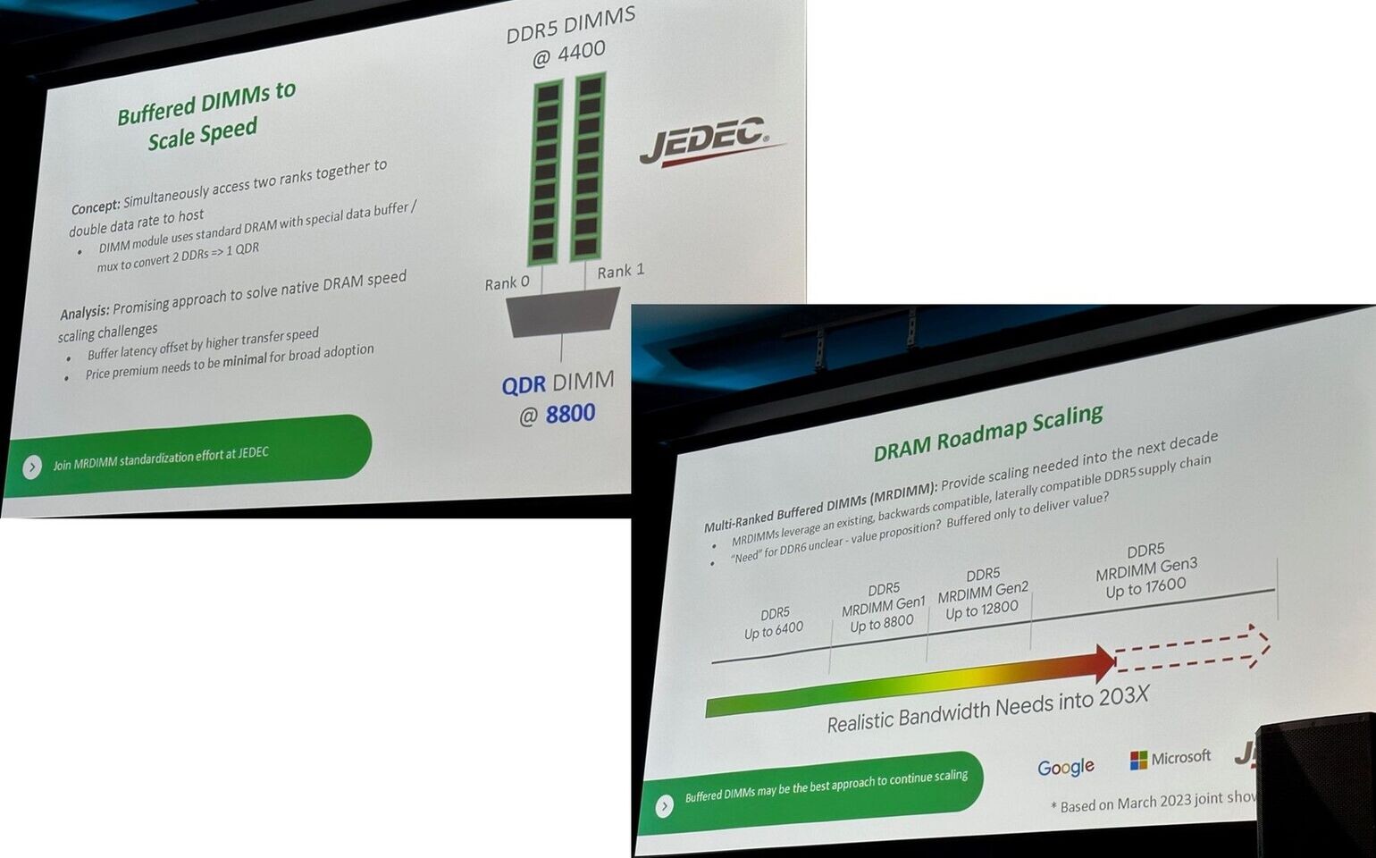
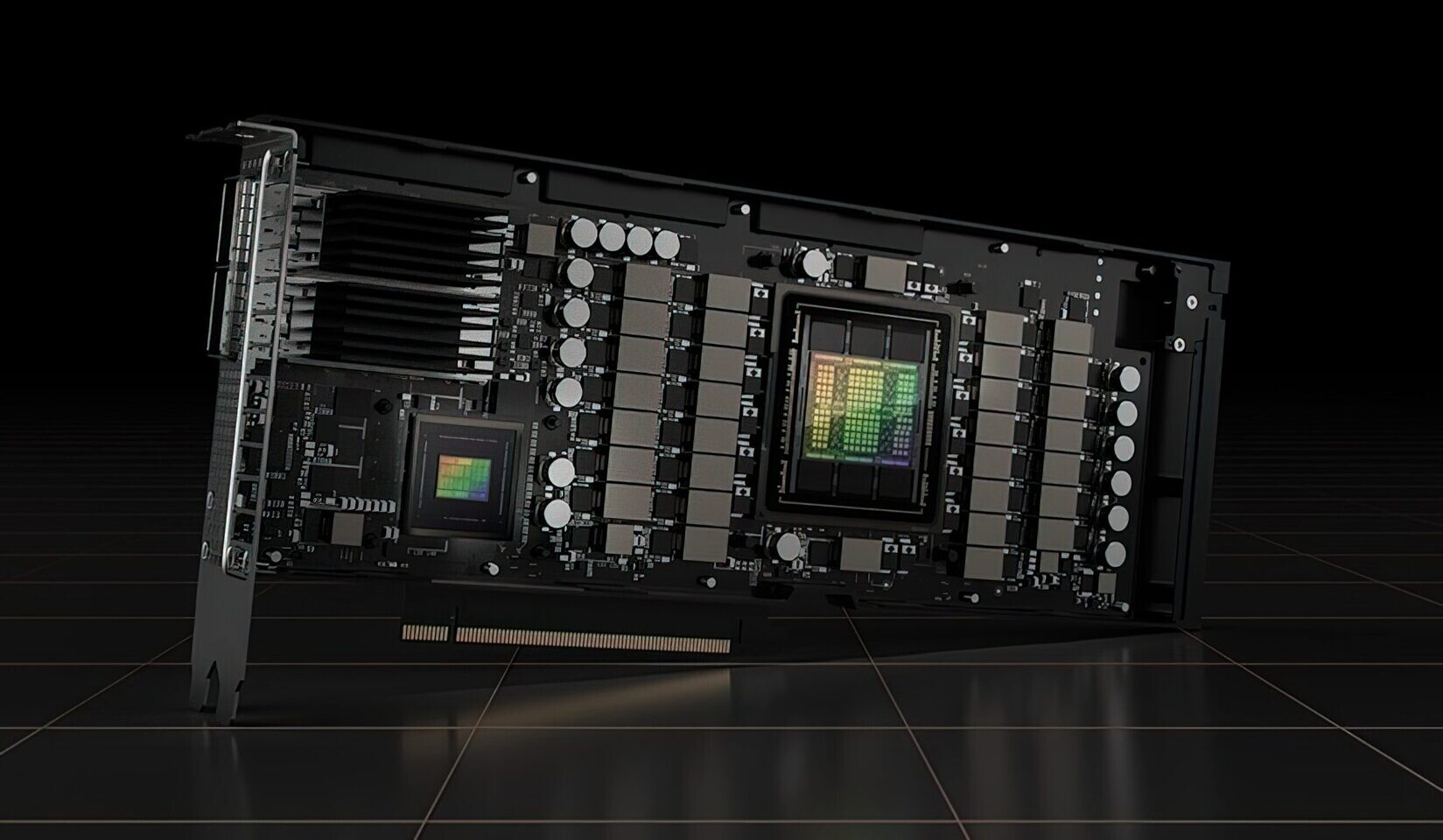
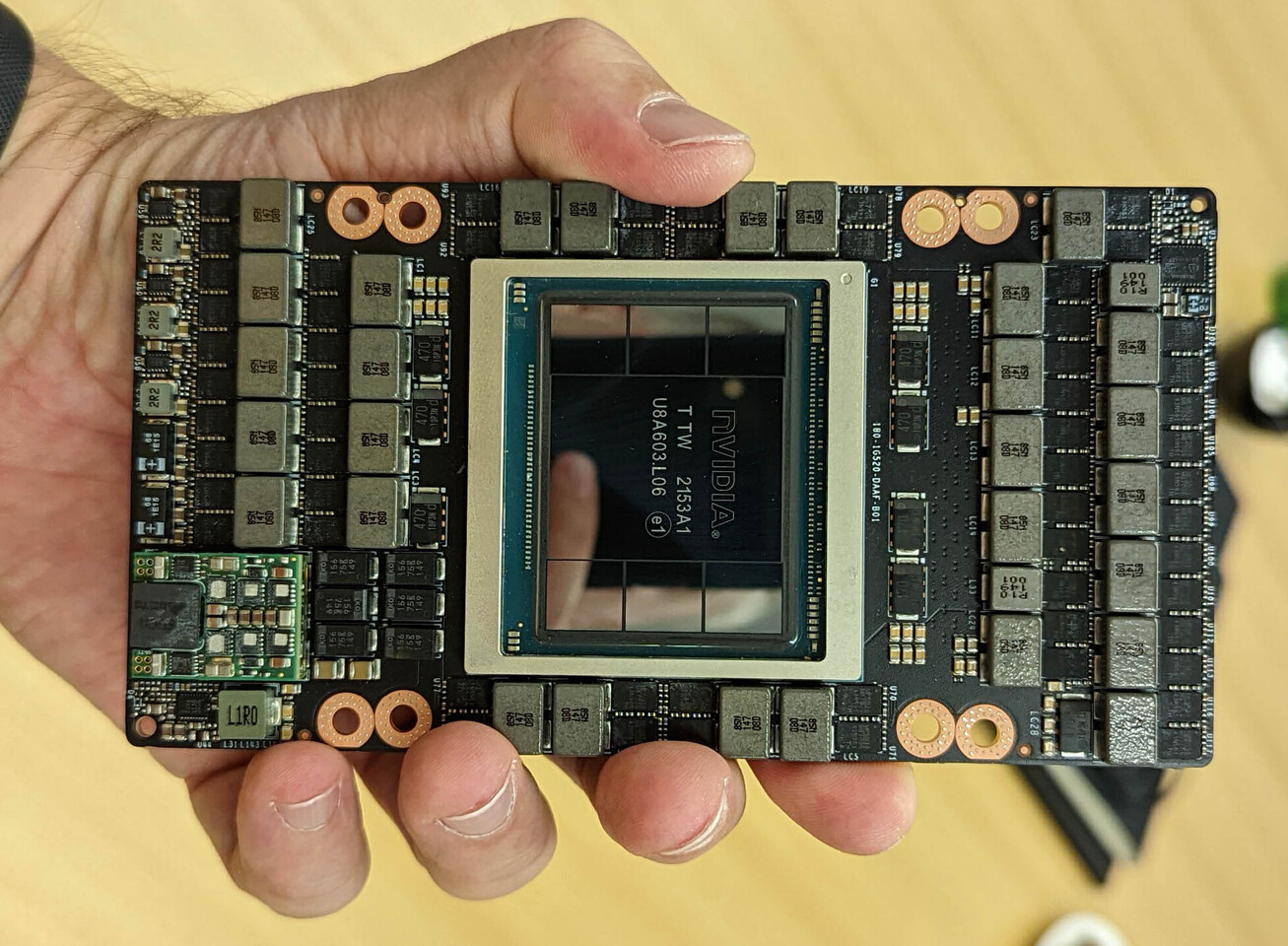
NVIDIA Allegedly Preparing H100 GPU with 94 and 64 GB Memory

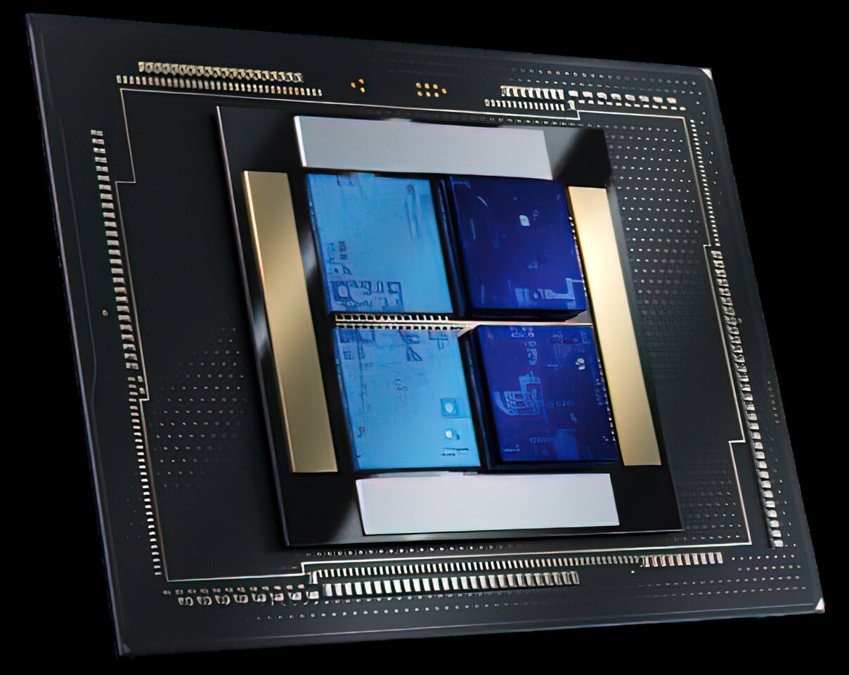
NVIDIA's compute and AI-oriented H100 GPU is supposedly getting an upgrade. The H100 GPU is NVIDIA's most powerful offering and comes in a few different flavors: H100 PCIe, H100 SXM, and H100 NVL (a duo of two GPUs). Currently, the H100 GPU comes with 80 GB of HBM2E, both in the PCIe and SXM5 version of the card. A notable exception if the H100 NVL, which comes with 188 GB of HBM3, but that is for two cards, making it 94 GB per each. However, we could see NVIDIA enable 94 and 64 GB options for the H100 accelerator soon, as the latest PCI ID Repository shows.

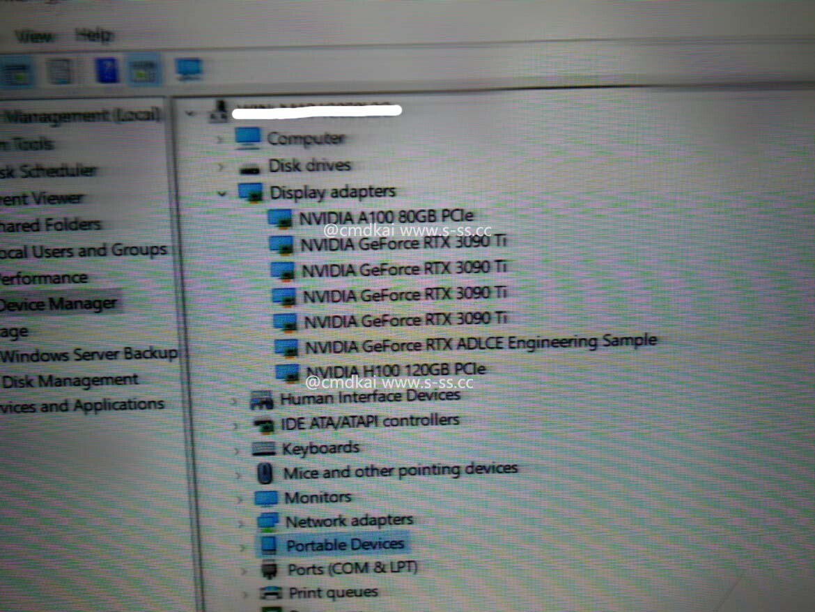
According to the PCI ID Repository listing, two messages are posted: "Kindly help to add H100 SXM5 64 GB into 2337." and "Kindly help to add H100 SXM5 94 GB into 2339." These two messages indicate that NVIDIA could prepare its H100 in more variations. In September 2022, we saw NVIDIA prepare an H100 variation with 120 GB of memory, but that still isn't official. These PCIe IDs could just come from engineering samples that NVIDIA is testing in the labs, and these cards could never appear on any market. So, we have to wait and see how it plays out.

Major CSPs Aggressively Constructing AI Servers and Boosting Demand for AI Chips and HBM, Advanced Packaging Capacity Forecasted to Surge 30~40%

TrendForce reports that explosive growth in generative AI applications like chatbots has spurred significant expansion in AI server development in 2023. Major CSPs including Microsoft, Google, AWS, as well as Chinese enterprises like Baidu and ByteDance, have invested heavily in high-end AI servers to continuously train and optimize their AI models. This reliance on high-end AI servers necessitates the use of high-end AI chips, which in turn will not only drive up demand for HBM during 2023~2024, but is also expected to boost growth in advanced packaging capacity by 30~40% in 2024.

TrendForce highlights that to augment the computational efficiency of AI servers and enhance memory transmission bandwidth, leading AI chip makers such as Nvidia, AMD, and Intel have opted to incorporate HBM. Presently, Nvidia's A100 and H100 chips each boast up to 80 GB of HBM2e and HBM3. In its latest integrated CPU and GPU, the Grace Hopper Superchip, Nvidia expanded a single chip's HBM capacity by 20%, hitting a mark of 96 GB. AMD's MI300 also uses HBM3, with the MI300A capacity remaining at 128 GB like its predecessor, while the more advanced MI300X has ramped up to 192 GB, marking a 50% increase. Google is expected to broaden its partnership with Broadcom in late 2023 to produce the AISC AI accelerator chip TPU, which will also incorporate HBM memory, in order to extend AI infrastructure.

Intel Falcon Shores is Initially a GPU, Gaudi Accelerators to Disappear

During the ISC High Performance 2023 international conference, Intel announced interesting roadmap updates to its high-performance computing (HPC) and artificial intelligence (AI). With the scrapping of Rialto Bridge and Lancaster Sound, Intel merged these accelerator lines into Falcon Shores processor for HPC and AI, initially claiming to be a CPU+GPU solution on a single package. However, during the ISC 2023 talk, the company forced a change of plans, and now, Falcon Shores is GPU only solution destined for a 2025 launch. Originally, Intel wanted to combine x86-64 cores with Xe GPU to form an "XPU" module that powers HPC and AI workloads. However, Intel did not see a point in forcing customers to choose between specific CPU-to-GPU core ratios that would need to be in an XPU accelerator. Instead, a regular GPU solution paired with a separate CPU is the choice of Intel for now. In the future, as workloads get more defined, XPU solutions are still a possibility, just delayed from what was originally intended.

Regarding Intel's Gaudi accelerators, the story is about to end. The company originally paid two billion US Dollars for Habana Labs and its Gaudi hardware. However, Intel now plans to stop the Gaudi development as a standalone accelerator and instead use the IP to integrate it into its Falcon Shores GPU. Using modular, tile-based architecture, the Falcon Shores GPU features standard ethernet switching, up to 288 GB of HBM3 running at 9.8 TB/s throughput, I/O optimized for scaling, and support for FP8 and FP16 floating point precision needed for AI and other workloads. As noted, the creation of XPU was premature, and now, the initial Falcon Shores GPU will become an accelerator for HPC, AI, and a mix of both, depending on a specific application. You can see the roadmap below for more information.

PMIC Issue with Server DDR5 RDIMMs Reported, Convergence of DDR5 Server DRAM Price Decline

TrendForce reports that mass production of new server platforms—such as Intel Sapphire Rapids and AMD Genoa—is imminent. However, recent market reports have indicated a PMIC compatibility issue for server DDR5 RDIMMs; DRAM suppliers and PMIC vendors are working to address the problem. TrendForce believes this will have two effects: First, DRAM suppliers will temporarily procure more PMICs from Monolithic Power Systems (MPS), which supplies PMICs without any issues. Second, supply will inevitably be affected in the short term as current DDR5 server DRAM production still uses older processes, which will lead to a convergence in the price decline of DDR5 server DRAM in 2Q23—from the previously estimated 15~20% to 13~18%.

As previously mentioned, PMIC issues and the production process relying on older processes are all having a short-term impact on the supply of DDR5 server DRAM. SK hynix has gradually ramped up production and sales of 1α-nm, which, unlike 1y-nm, has yet to be fully verified by consumers. Current production processes are still being dominated by Samsung and SK hynix's 1y-nm and Micron's 1z-nm; 1α and 1β-nm production is projected to increase in 2H23.

HBM Supply Leader SK Hynix's Market Share to Exceed 50% in 2023 Due to Demand for AI Servers

A strong growth in AI server shipments has driven demand for high bandwidth memory (HBM). TrendForce reports that the top three HBM suppliers in 2022 were SK hynix, Samsung, and Micron, with 50%, 40%, and 10% market share, respectively. Furthermore, the specifications of high-end AI GPUs designed for deep learning have led to HBM product iteration. To prepare for the launch of NVIDIA H100 and AMD MI300 in 2H23, all three major suppliers are planning for the mass production of HBM3 products. At present, SK hynix is the only supplier that mass produces HBM3 products, and as a result, is projected to increase its market share to 53% as more customers adopt HBM3. Samsung and Micron are expected to start mass production sometime towards the end of this year or early 2024, with HBM market shares of 38% and 9%, respectively.

AI server shipment volume expected to increase by 15.4% in 2023
NVIDIA's DM/ML AI servers are equipped with an average of four or eight high-end graphics cards and two mainstream x86 server CPUs. These servers are primarily used by top US cloud services providers such as Google, AWS, Meta, and Microsoft. TrendForce analysis indicates that the shipment volume of servers with high-end GPGPUs is expected to increase by around 9% in 2022, with approximately 80% of these shipments concentrated in eight major cloud service providers in China and the US. Looking ahead to 2023, Microsoft, Meta, Baidu, and ByteDance will launch generative AI products and services, further boosting AI server shipments. It is estimated that the shipment volume of AI servers will increase by 15.4% this year, and a 12.2% CAGR for AI server shipments is projected from 2023 to 2027.

AMD and JEDEC Create DDR5 MRDIMMs with 17,600 MT/s Speeds

AMD and JEDEC are collaborating to create a new industry standard for DDR5 memory called MRDIMMs (multi-ranked buffered DIMMs). The constant need for bandwidth in server systems provides trouble that can not easily be solved. Adding more memory is difficult, as motherboards can only get so big. Incorporating on-package memory solutions like HBM is expensive and can only scale to a specific memory capacity. However, engineers of JEDEC, with the help of AMD, have come to make a new standard that will try and solve this challenge using the new MRDIMM technology. The concept of MRDIMM is, on paper, straightforward. It combines two DDR5 DIMMs on a single module to effectively double the bandwidth. Specifically, if you take two DDR5 DIMMs running at 4,400 MT/s and connect them to create a single DIMM, you get 8,800 MT/s speeds on a single module. To efficiently use it, a special data mux or buffer will effectively take two Double Data Rate (DDR) DIMMs and convert them into Quad Data Rate (QDR) DIMMs.

The design also allows simultaneous access to both ranks of memory, thanks to the added mux. First-generation MRDIMMs can produce speeds of up to 8,800 MT/s, while the second and third generations modules can go to 12,800 MT/s and 17,600 MT/s, respectively. We expect third-generation MRDIMMs after 2030, so the project is still far away. Additionally, Intel has a similar solution called Multiplexer Combined Ranks DIMM (MCRDIMM) which uses a similar approach. However, Intel's technology is expected to see the light of the day as early as 2024/2025 and beyond the generation of servers, with Granite Rapids likely representing a contender for this technology. SK Hynix already makes MCRDIMMs, and you can see the demonstration of the approach below.

Intel Xeon Granite Rapids and Sierra Forest to Feature up to 500 Watt TDP and 12-Channel Memory

Today, thanks to Yuuki_Ans on the Chinese Bilibili forum, we have more information about the upcoming "Avenue City" platform that powers Granite Rapids and Sierra Forest. Intel's forthcoming Granite Rapids and Sierra Forest Xeon processors will diverge the Xeon family into two offerings: one optimized for performance/core equipped with P-cores and the other for power/core equipped with E-cores. The reference platform Intel designs and shares with OEMs internally is a 16.7" x 20" board with 20 PCB layers, made as a dual-socket solution. Featuring two massive LGA-7529 sockets, the reference design shows the basic layout for a server powered by these new Xeons.

Capable of powering Granite Rapids / Sierra Forest-AP processors of up to 500 Watts, the platform also accommodates next-generation I/O. Featuring 24 DDR5 DIMMs with support for 12-channel memory, with memory speeds of up to 6400 MT/s. The PCIe selection includes six PCIe Gen 5 x16 links supporting CXL cache coherent protocol and 6x24 UPI links. Additionally, we have another piece of information that Granite Rapids will come with up to 128 cores and 256 threads in both regular and HBM-powered Xeon Max flavoring. You can see storage and reference platform configuration details on the slides below.

Shipments of AI Servers Will Climb at CAGR of 10.8% from 2022 to 2026

According to TrendForce's latest survey of the server market, many cloud service providers (CSPs) have begun large-scale investments in the kinds of equipment that support artificial intelligence (AI) technologies. This development is in response to the emergence of new applications such as self-driving cars, artificial intelligence of things (AIoT), and edge computing since 2018. TrendForce estimates that in 2022, AI servers that are equipped with general-purpose GPUs (GPGPUs) accounted for almost 1% of annual global server shipments. Moving into 2023, shipments of AI servers are projected to grow by 8% YoY thanks to ChatBot and similar applications generating demand across AI-related fields. Furthermore, shipments of AI servers are forecasted to increase at a CAGR of 10.8% from 2022 to 2026.

AMD Envisions Stacked DRAM on top of Compute Chiplets in the Near Future

AMD in its ISSCC 2023 presentation detailed how it has advanced data-center energy-efficiency and managed to keep up with Moore's Law, even as semiconductor foundry node advances have tapered. Perhaps its most striking prediction for server processors and HPC accelerators is multi-layer stacked DRAM. The company has, for some time now, made logic products, such as GPUs, with stacked HBM. These have been multi-chip modules (MCMs), in which the logic die and HBM stacks sit on top of a silicon interposer. While this conserves PCB real-estate compared to discrete memory chips/modules; it is inefficient on the substrate, and the interposer is essentially a silicon die that has microscopic wiring between the chips stacked on top of it.

AMD envisions that the high-density server processor of the near-future will have many layers of DRAM stacked on top of logic chips. Such a method of stacking conserves both PCB and substrate real-estate, allowing chip-designers to cram even more cores and memory per socket. The company also sees a greater role of in-memory compute, where trivial simple compute and data-movement functions can be executed directly on the memory, saving round-trips to the processor. Lastly, the company talked about the possibility of an on-package optical PHY, which would simplify network infrastructure.

Giga Computing Announces Its GIGABYTE Server Portfolio for the 4th Gen Intel Xeon Scalable Processor

Giga Computing is an industry leader in high-performance servers and workstations, today announced the next-generation of GIGABYTE servers and server motherboards for the new 4th Gen Intel Xeon Scalable processor to achieve efficient performance gains with built-in accelerators. The new processors have the most built-in accelerators of any processor on the market to help maximize performance efficiency for emerging workloads; and do so while boosting virtualization and AI performance. Generational improvements make this platform ideal for AI, cloud computing, advanced analytics, HPC, networking, and storage applications. For these markets, Giga Computing has announced fourteen new series that constitute seventy-eight configurations for customers to choose from. And all these new GIGABYTE products support the full portfolio of 4th Gen Intel Xeon Scalable processors, including those with high bandwidth memory (HBM) in the Intel Xeon Max Series.

AMD Shows Instinct MI300 Exascale APU with 146 Billion Transistors

During its CES 2023 keynote, AMD announced its latest Instinct MI300 APU, a first of its kind in the data center world. Combining the CPU, GPU, and memory elements into a single package eliminates latency imposed by long travel distances of data from CPU to memory and from CPU to GPU throughout the PCIe connector. In addition to solving some latency issues, less power is needed to move the data and provide greater efficiency. The Instinct MI300 features 24 Zen4 cores with simultaneous multi-threading enabled, CDNA3 GPU IP, and 128 GB of HBM3 memory on a single package. The memory bus is 8192-bit wide, providing unified memory access for CPU and GPU cores. CLX 3.0 is also supported, making cache-coherent interconnecting a reality.

The Instinct MI300 APU package is an engineering marvel of its own, with advanced chiplet techniques used. AMD managed to do 3D stacking and has nine 5 nm logic chiplets that are 3D stacked on top of four 6 nm chiplets with HBM surrounding it. All of this makes the transistor count go up to 146 billion, representing the sheer complexity of a such design. For performance figures, AMD provided a comparison to Instinct MI250X GPU. In raw AI performance, the MI300 features an 8x improvement over MI250X, while the performance-per-watt is "reduced" to a 5x increase. While we do not know what benchmark applications were used, there is a probability that some standard benchmarks like MLPerf were used. For availability, AMD targets the end of 2023, when the "El Capitan" exascale supercomputer will arrive using these Instinct MI300 APU accelerators. Pricing is unknown and will be unveiled to enterprise customers first around launch.

AMD Explains the Economics Behind Chiplets for GPUs

AMD, in its technical presentation for the new Radeon RX 7900 series "Navi 31" GPU, gave us an elaborate explanation on why it had to take the chiplets route for high-end GPUs, devices that are far more complex than CPUs. The company also enlightened us on what sets chiplet-based packages apart from classic multi-chip modules (MCMs). An MCM is a package that consists of multiple independent devices sharing a fiberglass substrate.

An example of an MCM would be a mobile Intel Core processor, in which the CPU die and the PCH die share a substrate. Here, the CPU and the PCH are independent pieces of silicon that can otherwise exist on their own packages (as they do on the desktop platform), but have been paired together on a single substrate to minimize PCB footprint, which is precious on a mobile platform. A chiplet-based device is one where a substrate is made up of multiple dies that cannot otherwise independently exist on their own packages without an impact on inter-die bandwidth or latency. They are essentially what should have been components on a monolithic die, but disintegrated into separate dies built on different semiconductor foundry nodes, with a purely cost-driven motive.

Intel Introduces the Max Series Product Family: Ponte Vecchio and Sapphire Rapids

In advance of Supercomputing '22 in Dallas, Intel Corporation has introduced the Intel Max Series product family with two leading-edge products for high performance computing (HPC) and artificial intelligence (AI): Intel Xeon CPU Max Series (code-named Sapphire Rapids HBM) and Intel Data Center GPU Max Series (code-named Ponte Vecchio). The new products will power the upcoming Aurora supercomputer at Argonne National Laboratory, with updates on its deployment shared today.

The Xeon Max CPU is the first and only x86-based processor with high bandwidth memory, accelerating many HPC workloads without the need for code changes. The Max Series GPU is Intel's highest density processor, packing over 100 billion transistors into a 47-tile package with up to 128 gigabytes (GB) of high bandwidth memory. The oneAPI open software ecosystem provides a single programming environment for both new processors. Intel's 2023 oneAPI and AI tools will deliver capabilities to enable the Intel Max Series products' advanced features.

Eliyan Closes $40M Series A Funding Round and Unveils Industry's Highest Performance Chiplet Interconnect Technologies

Eliyan Corporation, credited for the invention of the semiconductor industry's highest-performance and most efficient chiplet interconnect, today announced two major milestones in the commercialization of its technology for multi-die chiplet integration: the close of its Series A $40M funding round, and the successful tapeout of its technology on an industry standard 5-nanometer (nm) process.

Eliyan's NuLink PHY and NuGear technologies address the critical need for a commercially viable approach to enabling high performance and cost-effectiveness in the connection of homogeneous and heterogenous architectures on a standard, organic chip substrate. It has proven to achieve similar bandwidth, power efficiency, and latency as die-to-die implementations using advanced packaging technologies, but without the other drawbacks of specialized approaches.

NVIDIA Could Launch Hopper H100 PCIe GPU with 120 GB Memory

NVIDIA's high-performance computing hardware stack is now equipped with the top-of-the-line Hopper H100 GPU. It features 16896 or 14592 CUDA cores, developing if it comes in SXM5 of PCIe variant, with the former being more powerful. Both variants come with a 5120-bit interface, with the SXM5 version using HBM3 memory running at 3.0 Gbps speed and the PCIe version using HBM2E memory running at 2.0 Gbps. Both versions use the same capacity capped at 80 GBs. However, that could soon change with the latest rumor suggesting that NVIDIA could be preparing a PCIe version of Hopper H100 GPU with 120 GBs of an unknown type of memory installed.

According to the Chinese website "s-ss.cc" the 120 GB variant of the H100 PCIe card will feature an entire GH100 chip with everything unlocked. As the site suggests, this version will improve memory capacity and performance over the regular H100 PCIe SKU. With HPC workloads increasing in size and complexity, more significant memory allocation is needed for better performance. With the recent advances in Large Language Models (LLMs), AI workloads use trillions of parameters for tranining, most of which is done on GPUs like NVIDIA H100.

AMD Instinct MI300 APU to Power El Capitan Exascale Supercomputer

The Exascale supercomputing race is now well underway, as the US-based Frontier supercomputer got delivered, and now we wait to see the remaining systems join the race. Today, during 79th HPC User Forum at Oak Ridge National Laboratory (ORNL), Terri Quinn at Lawrence Livermore National Laboratory (LLNL) delivered a few insights into what El Capitan exascale machine will look like. And it seems like the new powerhouse will be based on AMD's Instinct MI300 APU. LLNL targets peak performance of over two exaFLOPs and a sustained performance of more than one exaFLOP, under 40 megawatts of power. This should require a very dense and efficient computing solution, just like the MI300 APU is.

As a reminder, the AMD Instinct MI300 is an APU that combines Zen 4 x86-64 CPU cores, CDNA3 compute-oriented graphics, large cache structures, and HBM memory used as DRAM on a single package. This is achieved using a multi-chip module design with 2.5D and 3D chiplet integration using Infinity architecture. The system will essentially utilize thousands of these APUs to become one large Linux cluster. It is slated for installation in 2023, with an operating lifespan from 2024 to 2030.

AMD CDNA3 Architecture Sees the Inevitable Fusion of Compute Units and x86 CPU at Massive Scale

AMD in its 2022 Financial Analyst Day presentation unveiled its next-generation CDNA3 compute architecture, which will see something we've been expecting for a while—a compute accelerator that has a large number of compute units for scalar processing, and a large number of x86-64 CPU cores based on some future "Zen" microarchitecture, onto a single package. The presence of CPU cores on the package would eliminate the need for the system to have an EPYC or Xeon processor at its head, and clusters of Instinct CDNA3 processors could run themselves without the need for a CPU and its system memory.

The Instinct CDNA3 processor will feature an advanced packaging technology that brings various IP blocks together as chiplets, each based on a node most economical to it, without compromising on its function. The package features stacked HBM memory, and this memory is shared not just by the compute units and x86 cores, but also forms part of large shared memory pools accessible across packages. 4th Generation Infinity Fabric ties it all together.

Samsung & Red Hat Announce Collaboration in the Field of Next-Generation Memory Software

Samsung Electronics and Red Hat today announced a broad collaboration on software technologies for next-generation memory solutions. The partnership will focus on the development and validation of open source software for existing and emerging memory and storage products, including NVMe SSDs; CXL memory; computational memory/storage (HBM-PIM, Smart SSDs) and fabrics — in building an expansive ecosystem for closely integrated memory hardware and software. The exponential growth of data driven by AI, AR and the fast-approaching metaverse is bringing disruptive changes to memory designs, requiring more sophisticated software technologies that better link with the latest hardware advancements.

"Samsung and Red Hat will make a concerted effort to define and standardize memory software solutions that embrace evolving server and memory hardware, while building a more robust memory ecosystem," said Yongcheol Bae, Executive Vice President and Head of the Memory Application Engineering Team at Samsung Electronics. "We will invite partners from across the IT industry to join us in expanding the software-hardware memory ecosystem to create greater customer value."

Alleged AMD Instinct MI300 Exascale APU Features Zen4 CPU and CDNA3 GPU

Today we got information that AMD's upcoming Instinct MI300 will be allegedly available as an Accelerated Processing Unit (APU). AMD APUs are processors that combine CPU and GPU into a single package. AdoredTV managed to get ahold of a slide that indicates that AMD Instinct MI300 accelerator will also come as an APU option that combines Zen4 CPU cores and CDNA3 GPU accelerator in a single, large package. With technologies like 3D stacking, MCM design, and HBM memory, these Instinct APUs are positioned to be a high-density compute the product. At least six HBM dies are going to be placed in a package, with the APU itself being a socketed design.

The leaked slide from AdoredTV indicates that the first tapeout is complete by the end of the month (presumably this month), with the first silicon hitting AMD's labs in Q3 of 2022. If the silicon turns out functional, we could see these APUs available sometime in the first half of 2023. Below, you can see an illustration of the AMD Instinct MI300 GPU. The APU version will potentially be of the same size with Zen4 and CDNA3 cores spread around the package. As Instinct MI300 accelerator is supposed to use eight compute tiles, we could see different combinations of CPU/GPU tiles offered. As we await the launch of the next-generation accelerators, we are yet to see what SKUs AMD will bring.

Intel Meteor Lake, HBM2E-enabled Sapphire Rapids, and Ponte Vecchio Pictured

Intel has allowed the media to get a closer look at the next generation of silicon that will power millions of systems in years to come during its private Vision event. PC Watch, a Japanese tech media, managed to get some shots of the upcoming Meteor Lake, Sapphire Rapids, and Ponte Vecchio processors. Starting with Meteor Lake, Intel has displayed two packages for this processor family. The first one is the ultra-compact, high-density UP9 package used for highly compact mobile systems, and it is made out of silicon with minimal packaging to save space. The second one is a traditional design with more oversized packaging, designed for typical laptop/notebook configurations.

NVIDIA H100 SXM Hopper GPU Pictured Up Close

ServeTheHome, a tech media outlet focused on everything server/enterprise, posted an exclusive set of photos of NVIDIA's latest H100 "Hopper" accelerator. Being the fastest GPU NVIDIA ever created, H100 is made on TSMC's 4 nm manufacturing process and features over 80 billion transistors on an 814 mm² CoWoS package designed by TSMC. Complementing the massive die, we have 80 GB of HBM3 memory that sits close to the die. Pictured below, we have an SXM5 H100 module packed with VRM and power regulation. Given that the rated TDP for this GPU is 700 Watts, power regulation is a serious concern and NVIDIA managed to keep it in check.

On the back of the card, we see one short and one longer mezzanine connector that acts as a power delivery connector, different from the previous A100 GPU layout. This board model is labeled PG520 and is very close to the official renders that NVIDIA supplied us with on launch day.

SK Hynix Presents HBM3 DRAM at NVIDIA GTC 2022

SK hynix, was the only company that presented its HBM3, a high-end product known as the fastest DRAM in existence with the biggest capacity, at NVIDIA GTC (GPU Technology Conference) 2022, which took place on March 21~24. Known as the world's best-performing DRAM, HBM3 is the fourth generation of the HBM (High Bandwidth Memory) technology. SK hynix's HBM3 uses over 8,000 TSVs per stack (i.e. over 100,000 TSVs in a 12-Hi stack) and can feature up to 12-Hi stack, which is an upgrade from the previous HBM2E's 8-Hi stack. When fully stacked, it can offer up to 24 GB of capacity. With a 16-channel architecture, it runs at 6.4 Gbps, which is double that of HBM2E and which is the fastest in the world, expecting to further accelerate our digital life.

For instance, HBM has become a prerequisite for the Levels 4 and 5 of driving automation when it comes to autonomous vehicles, a topic that has garnered a great deal of attention nowadays. Also, HBM3 is expected to play an even bigger role along with the growth of High Performance Computing (HPC), Artificial Intelligence (AI), Machine Learning (ML), and Advanced Driver Assistance Systems (ADAS) markets fueled by the acceleration of digital transformation.

Intel Details Ponte Vecchio Accelerator: 63 Tiles, 600 Watt TDP, and Lots of Bandwidth

During the International Solid-State Circuits Conference (ISSCC) 2022, Intel gave us a more significant look at its upcoming Ponte Vecchio HPC accelerator and how it operates. So far, Intel convinced us that the company created Ponte Vecchio out of 47 tiles glued together in one package. However, the ISSCC presentation shows that the accelerator is structured rather interestingly. There are 63 tiles in total, where 16 are reserved for compute, eight are used for RAMBO cache, two are Foveros base tiles, two represent Xe-Link tiles, eight are HBM2E tiles, and EMIB connection takes up 11 tiles. This totals for about 47 tiles. However, an additional 16 thermal tiles used in Ponte Vecchio regulate the massive TDP output of this accelerator.

What is interesting is that Intel gave away details of the RAMBO cache. This novel SRAM technology uses four banks of 3.75 MB groups total of 15 MB per tile. They are connected to the fabric at 1.3 TB/s connection per chip. In contrast, compute tiles are connected at 2.6 TB/s speeds to the chip fabric. With eight RAMBO cache tiles, we get an additional 120 MB SRAM present. The base tile is a 646 mm² die manufactured in Intel 7 semiconductor process and contains 17 layers. It includes a memory controller, the Fully Integrated Voltage Regulators (FIVR), power management, 16-lane PCIe 5.0 connection, and CXL interface. The entire area of Ponte Vecchio is rather impressive, as 47 active tiles take up 2,330 mm², whereas when we include thermal dies, the total area jumps to 3,100 mm². And, of course, the entire package is much larger at 4,844 mm², connected to the system with 4,468 pins.

Intel Updates Technology Roadmap with Data Center Processors and Game Streaming Service

At Intel's 2022 Investor Meeting, Chief Executive Officer Pat Gelsinger and Intel's business leaders outlined key elements of the company's strategy and path for long-term growth. Intel's long-term plans will capitalize on transformative growth during an era of unprecedented demand for semiconductors. Among the presentations, Intel announced product roadmaps across its major business units and key execution milestones, including: Accelerated Computing Systems and Graphics, Intel Foundry Services, Software and Advanced Technology, Network and Edge, Technology Development, More: For more from Intel's Investor Meeting 2022, including the presentations and news, please visit the Intel Newsroom and Intel.com's Investor Meeting site.

JEDEC Publishes HBM3 Update to High Bandwidth Memory (HBM) Standard

JEDEC Solid State Technology Association, the global leader in the development of standards for the microelectronics industry, today announced the publication of the next version of its High Bandwidth Memory (HBM) DRAM standard: JESD238 HBM3, available for download from the JEDEC website. HBM3 is an innovative approach to raising the data processing rate used in applications where higher bandwidth, lower power consumption and capacity per area are essential to a solution's market success, including graphics processing and high-performance computing and servers.
Return to Keyword Browsing
May 21st, 2024 21:40 EDT change timezone

New Forum Posts

Popular Reviews

Controversial News Posts