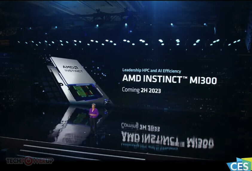
Two-ExaFLOP El Capitan Supercomputer Starts Installation Process with AMD Instinct MI300A
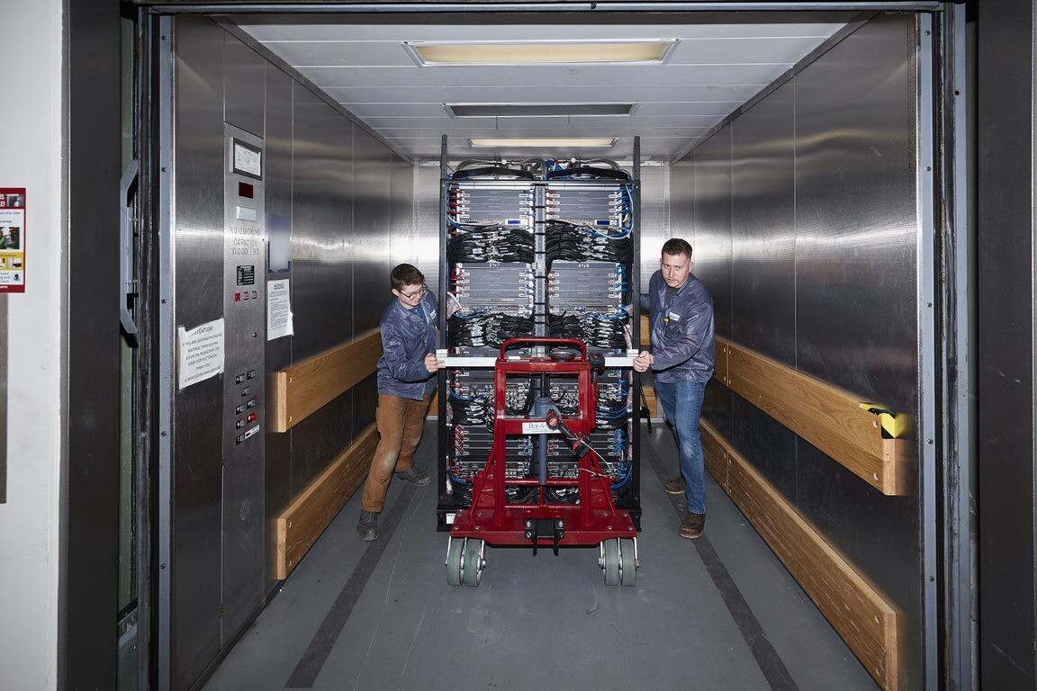
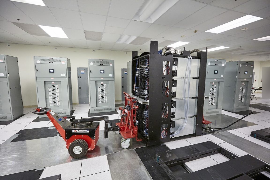
When Lawrence Livermore National Laboratory (LLNL) announced the creation of a two-ExaFLOP supercomputer named El Capitan, we heard that AMD would power it with its Instinct MI300 accelerator. Today, LNLL published a Tweet that states, "We've begun receiving & installing components for El Capitan, @NNSANews' first #exascale #supercomputer. While we're still a ways from deploying it for national security purposes in 2024, it's exciting to see years of work becoming reality." As published images show, HPE racks filled with AMD Instinct MI300 are showing up now at LNLL's facility, and the supercomputer is expected to go operational in 2024. This could mean that November 2023 TOP500 list update wouldn't feature El Capitan, as system enablement would be very hard to achieve in four months until then.
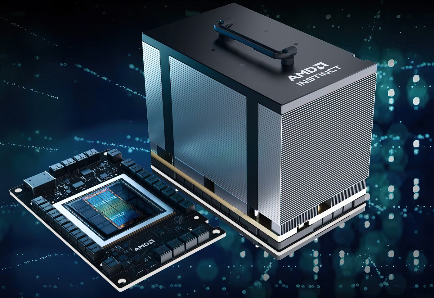
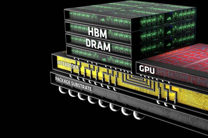
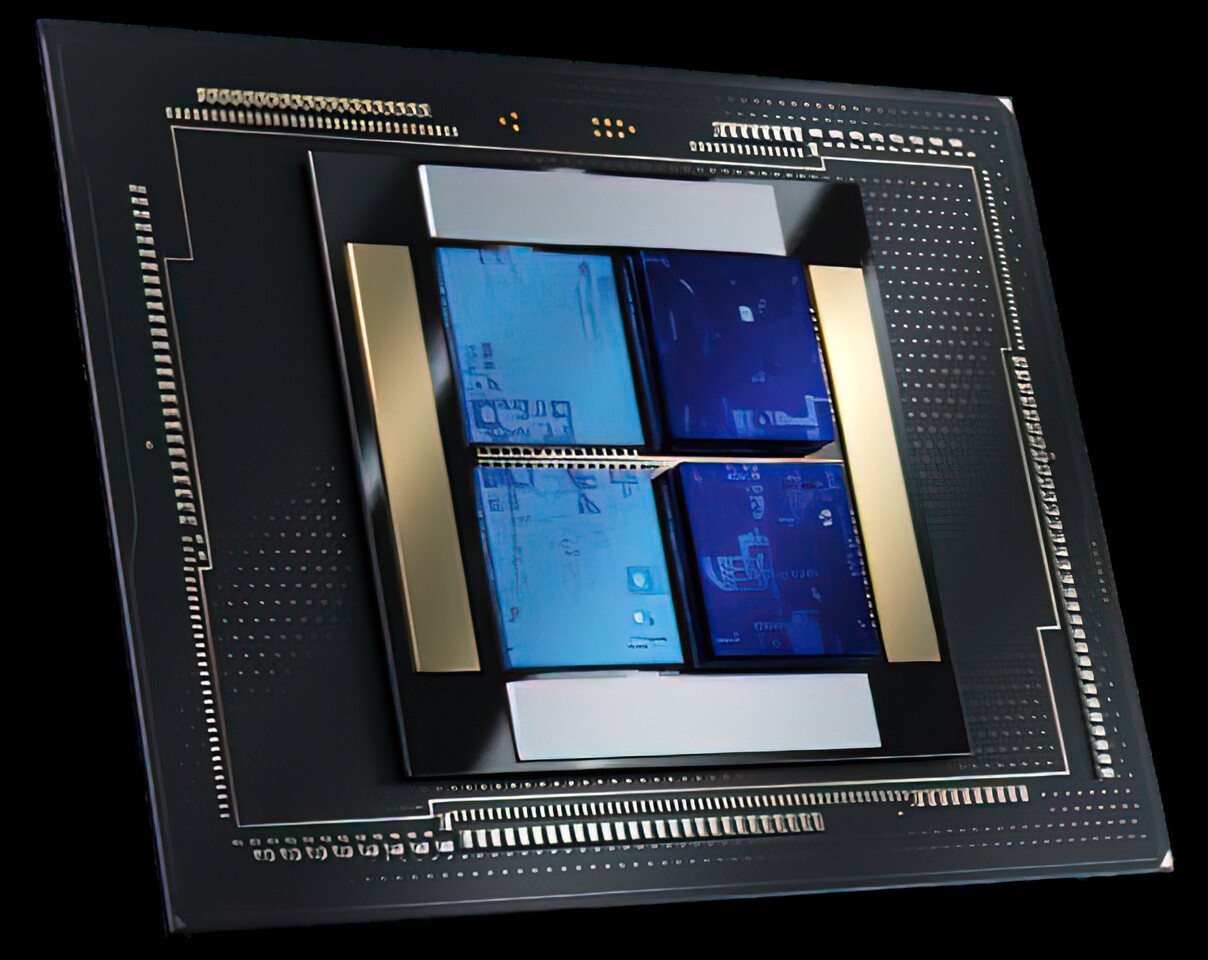
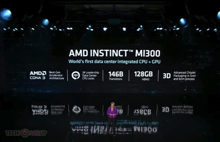
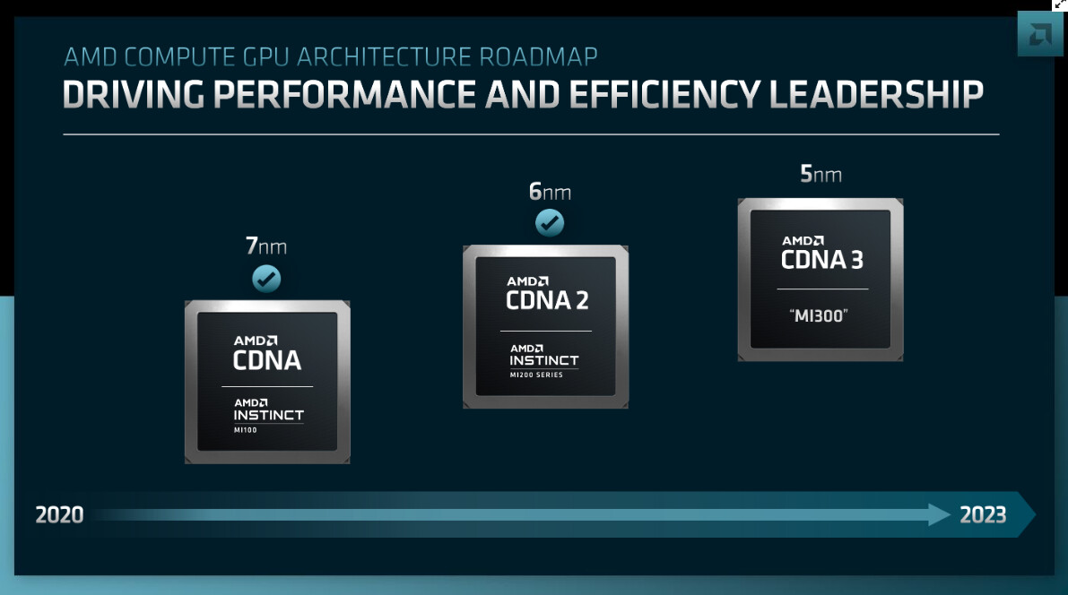
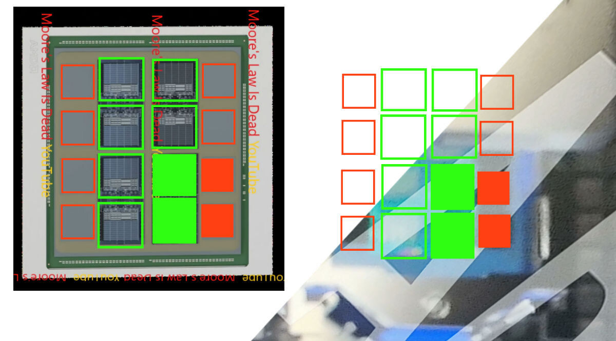
The El Capitan supercomputer is expected to run on AMD Instinct MI300A accelerator, which features 24 Zen4 cores, CDNA3 architecture, and 128 GB of HBM3 memory. All paired together in a four-accelerator configuration goes inside each node from HPE, also getting water cooling treatment. While we don't have many further details on the memory and storage of El Capitan, we know that the system will exceed two ExFLOPS at peak and will consume close to 40 MW of power.


The El Capitan supercomputer is expected to run on AMD Instinct MI300A accelerator, which features 24 Zen4 cores, CDNA3 architecture, and 128 GB of HBM3 memory. All paired together in a four-accelerator configuration goes inside each node from HPE, also getting water cooling treatment. While we don't have many further details on the memory and storage of El Capitan, we know that the system will exceed two ExFLOPS at peak and will consume close to 40 MW of power.