News Posts matching #HBM

Return to Keyword Browsing

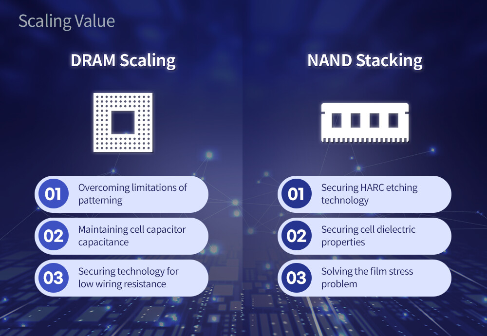
NVIDIA CMP 170HX Mining Card Tested, Based on GA100 GPU SKU

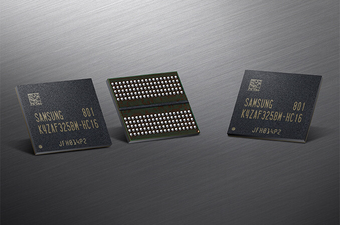
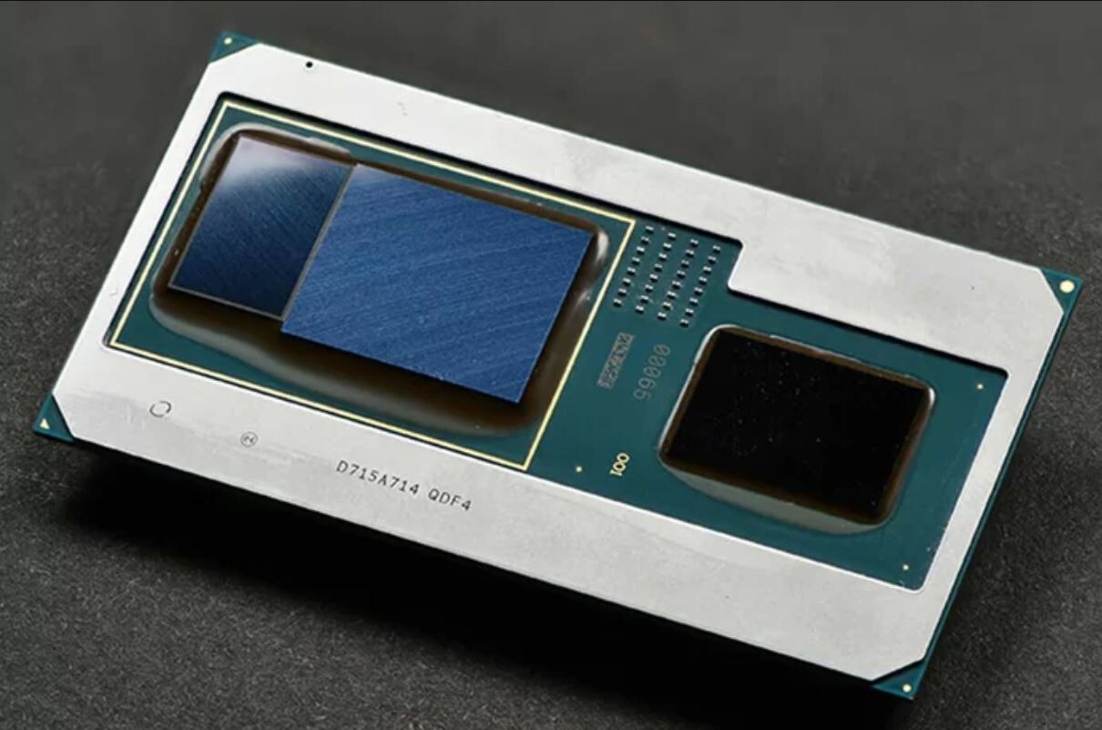
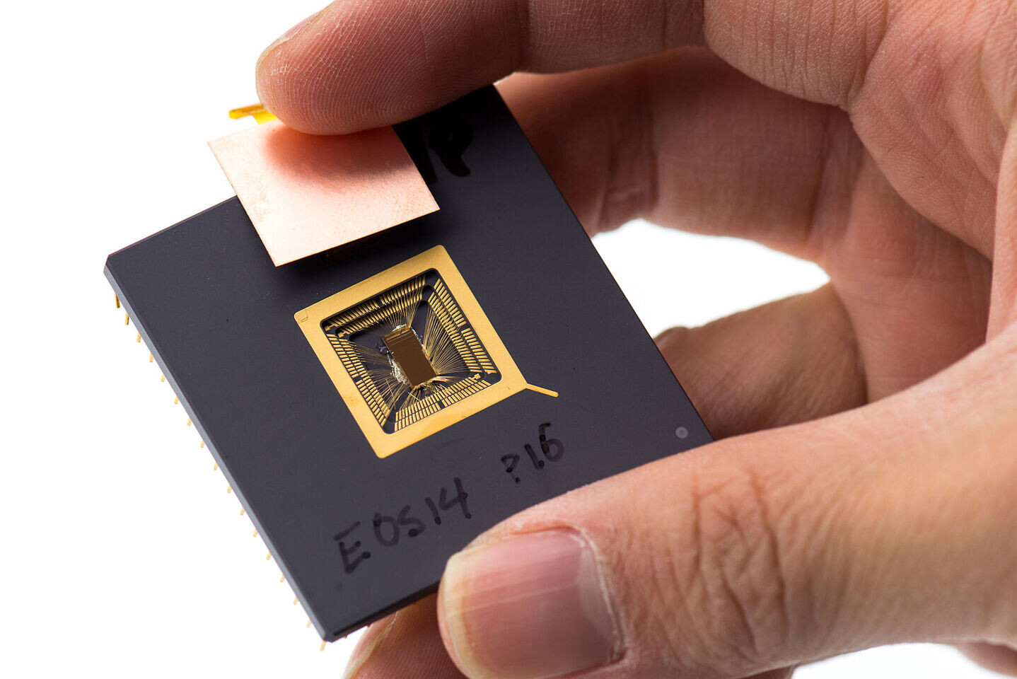
NVIDIA's Crypto Mining (CMP) series of graphics cards are made to work only for one purpose: mining cryptocurrency coins. Hence, their functionality is somewhat limited, and they can not be used for gaming as regular GPUs can. Today, Linus Tech Tips got ahold of NVIDIA's CMP 170HX mining card, which is not listed on the company website. According to the source, the card runs on NVIDIA's GA100-105F GPU, a version based on the regular GA100 SXM design used in data-center applications. Unlike its bigger brother, the GA100-105F SKU is a cut-down design with 4480 CUDA cores and 8 GB of HBM2E memory. The complete design has 6912 cores and 40/80 GB HBM2E memory configurations.

As far as the reason for choosing 8 GB HBM2E memory goes, we know that the Ethereum DAG file is under 5 GB, so the 8 GB memory buffer is sufficient for mining any coin out there. It is powered by an 8-pin CPU power connector and draws about 250 Watts of power. It can be adjusted to 200 Watts while retaining the 165 MH/s hash rate for Ethereum. This reference design is manufactured by NVIDIA and has no active cooling, as it is meant to be cooled in high-density server racks. Only a colossal heatsink is attached, meaning that the cooling needs to come from a third party. As far as pricing is concerned, Linus managed to get this card for $5000, making it a costly mining option.
More images follow...

Samsung Talks DDR6-12800, GDDR7 Development, and HBM3 Volume Production

During Samsung's Tech Day 2021, the company presented some interesting insights about the future of system memory technologies and how it plans to execute its production. Starting with the latest DDR5 standard, the company intends to follow JEDEC documents and offer some overclocking modules that surpass the specification advised by JEDEC. While the DDR5 standard specifies memory modules with 6,400 MT/s, Samsung will develop modules capable of overclocking up to 8,400 MT/s. These are not yet confirmed as they are still in the development phase. However, we can expect to see them in the later life of DDR5 memory.

The company also talked about the DDR6 standard, which is supposedly twice as fast as DDR5. The new DDR6 standard is still in early development, and all we know so far is that the number of memory channels per module is seeing a twofold increase over DDR5 to four channels. The number of memory banks also increases to 64. In addition to DDR6 for desktop and server use cases, the company is also working on Low Power DDR6 (LPDDR6) for mobile applications. While the company's LPDDR5 memory goes into volume production using the 1a-nm process at the beginning of 2022, the LPDDR6 is still in early development. The base speed for DDR6 modules will allegedly arrive at 12,800 MT/s, while overclocking modules will join the party at up to 17,000 MT/s. Mobile-oriented LPDDR6 version is also supposed to come with up to 17,000 MT/s speeds.

Intel Aurora Supercomputer Will Touch 2 ExaFLOPs of Computational Power

Intel's Aurora supercomputer is a $500 million contract with the US Department of Energy to deliver an exascale supercomputer for Argonne National Laboratory. The project aims to build a machine capable of cranking over one ExaFLOP of computing at sustained workloads. The supercomputer aims to reach two ExaFLOPs of computing power once the installation system is completed and powered. The contract bound Intel to create accelerators that are powerful enough to achieve this magical number. However, they left Intel with room to do a little bit extra. With Ponte Vecchio GPU behind the project, it seems like the GPU is performing better than expected.

According to Intel's CEO, Pat Gelsinger, the system will reach over 2 ExaFLOPs at peak and a bit below in sustained workloads. As per preliminary calculations done by The Next Platform, the system's estimations point towards 2.43 ExaFLOPs peak and around 1.7 ExaFLOPs in sustained workloads at Double-precision floating-point format math, aka FP64. The system will utilize Intel Xeon Sapphire Rapids processors with HBM memory and the powerful Ponte Vecchio GPU with 47 tiles and over 100 billion transistors.

SK hynix Announces Development of HBM3 DRAM

SK hynix Inc. announced that it has become the first in the industry to successfully develop the High Bandwidth Memory 3, the world's best-performing DRAM. HBM3, the fourth generation of the HBM technology with a combination of multiple DRAM chips vertically connected, is a high value product that innovatively raises the data processing rate.

The latest development, which follows the start of mass production of HBM2E in July last year, is expected to help consolidate the company's leadership in the market. SK hynix was also the first in the industry to start mass production of HBM2E. SK hynix's HBM3 is not only the fastest DRAM in the world, but also comes with the biggest capacity and significantly improved level of quality.

Synopsys Accelerates Multi-Die Designs with Industry's First Complete HBM3 IP and Verification Solutions

Synopsys, Inc. today announced the industry's first complete HBM3 IP solution, including controller, PHY, and verification IP for 2.5D multi-die package systems. HBM3 technology helps designers meet essential high-bandwidth and low-power memory requirements for system-on-chip (SoC) designs targeting high-performance computing, AI and graphics applications. Synopsys' DesignWare HBM3 Controller and PHY IP, built on silicon-proven HBM2E IP, leverage Synopsys' interposer expertise to provide a low-risk solution that enables high memory bandwidth at up to 921 GB/s.

The Synopsys verification solution, including Verification IP with built-in coverage and verification plans, off-the-shelf HBM3 memory models for ZeBu emulation, and HAPS prototyping system, accelerates verification from HBM3 IP to SoCs. To accelerate development of HBM3 system designs, Synopsys' 3DIC Compiler multi-die design platform provides a fully integrated architectural exploration, implementation and system-level analysis solution.

Jingjia Micro JM9 GPU Series Targeting GTX 1080 Performance Tapes Out

The Chinese Electronics company Jingjia Micro have recently completed the tapeout of their JM9 GPU series almost 2 years after they first announced the lineup. The JM9 series will consist of two GPUs with the entry-level JM9231 targeting GTX 1050 performance while the higher-end JM9271 aims for the GTX 1080. The JM9231 is stated to feature a clock speed above 1.5 GHz, 8 GB of GDDR5 memory, and will provide 2 TFLOPS of performance within a 150 W TDP through a PCIe Gen3 x16 interface. The JM9271 increases the clock speed to above 1.8 GHz and is paired with 16 GB of HBM memory which should offer 8 TFLOPS of single-precision performance to rival the GTX 1080. The card manages to do this within a TDP package of 200 W and also includes PCIe Gen4 x16 support. The two cards both support HDMI 2.0 in addition to DisplayPort 1.3 for the JM9231 and DisplayPort 1.4 for the JM9271.

While the JM9271 may target GTX 1080 performance it only features OpenGL and OpenCL API support lacking DirectX or Vulkan compatibility greatly reducing its use for gaming. The cards were originally expected to be available in 2020 but after various delays they are now ready to enter production. These products are highly unlikely to make their way outside of the Chinese mainland and if they did we wouldn't expect them to have much impact on the global market.

First AMD Radeon Vega M Drivers for Intel NUC8i7HNK and NUC8i7HVK in Over 16 Months Released

Intel and AMD released the first Radeon Software drivers for the exotic Radeon Vega M graphics found in Intel NUC8i7HNK and NUC8i7HVK, in over 16 months. The Intel Download Center just added version 21.10.03.11 of Radeon Software for the graphics solution, dated 09/09/2021. The previous drivers dated all the way back to February 2020, and were based on Adrenalin 20.2.

The drivers are based on a release candidate of Adrenalin 21.10, which is 21.10RC1, but does not include the security updates AMD could be bundling with the upcoming 21.10 drivers (October 2021). "Radeon RX Vega M Graphics Driver version 21.10.03.11, which is based on 21.10RC1, does not include the latest functional and security updates. An update is targeted to be released in March of 2022 and will include additional functional and security updates. Customers should update to the latest version as it becomes available," says Intel in the release notes of the drivers. The drivers do include optimization for the latest games, including "Metro Exodus" (DX12), and "Resident Evil Village," besides adding support for Microsoft PlayReady AV1 decode.

DOWNLOAD: AMD Radeon Vega M drivers for Intel NUC8i7HNK and NUC8i7HVK from Intel

Penetration Rate of Ice Lake CPUs in Server Market Expected to Surpass 30% by Year's End as x86 Architecture Remains Dominant, Says TrendForce

While the server industry transitions to the latest generation of processors based on the x86 platform, the Intel Ice Lake and AMD Milan CPUs entered mass production earlier this year and were shipped to certain customers, such as North American CSPs and telecommunication companies, at a low volume in 1Q21, according to TrendForce's latest investigations. These processors are expected to begin seeing widespread adoption in the server market in 3Q21. TrendForce believes that Ice Lake represents a step-up in computing performance from the previous generation due to its higher scalability and support for more memory channels. On the other hand, the new normal that emerged in the post-pandemic era is expected to drive clients in the server sector to partially migrate to the Ice Lake platform, whose share in the server market is expected to surpass 30% in 4Q21.

Certain Intel Xeon "Sapphire Rapids" SKUs Come with On-Package HBM

Intel today, in its 2021 International Supercomputing Conference presentation, revealed that certain next-generation Xeon "Sapphire Rapids" SKUs come with on-package high-bandwidth memory (HBM). Given the context of its presentation, these could be special SKUs designed for high-density HPC setups, in which the processor package includes certain amount of "PMEM" (package memory), besides the processor's 8-channel DDR5 memory interface.

The size of the HBM PMEM, and its position in the memory hierarchy, were detailed, too. Given its high-density applications, PMEM may not serve as a victim cache for the processor, but rather be capable of serving as main memory, with none of the DDR5 DRAM channels populated with DIMMs. On machines with DIMMs, the PMEM will serve as a victim cache for the processor's on-die last-level cache, accelerating the memory I/O. "The next-generation of Intel Xeon Scalable processors (code-named "Sapphire Rapids) will offer integrated High Bandwidth Memory (HBM), providing a dramatic boost in memory bandwidth and a significant performance improvement for HPC applications that operate memory bandwidth-sensitive workloads. Users can power through workloads using just High Bandwidth Memory or in combination with DDR5," says Intel.

New Intel XPU Innovations Target HPC and AI

At the 2021 International Supercomputing Conference (ISC) Intel is showcasing how the company is extending its lead in high performance computing (HPC) with a range of technology disclosures, partnerships and customer adoptions. Intel processors are the most widely deployed compute architecture in the world's supercomputers, enabling global medical discoveries and scientific breakthroughs. Intel is announcing advances in its Xeon processor for HPC and AI as well as innovations in memory, software, exascale-class storage, and networking technologies for a range of HPC use cases.

"To maximize HPC performance we must leverage all the computer resources and technology advancements available to us," said Trish Damkroger, vice president and general manager of High Performance Computing at Intel. "Intel is the driving force behind the industry's move toward exascale computing, and the advancements we're delivering with our CPUs, XPUs, oneAPI Toolkits, exascale-class DAOS storage, and high-speed networking are pushing us closer toward that realization."

NVIDIA Launches A100 PCIe-Based Accelerator with 80 GB HBM2E Memory

During this year's ISC 2021 event, as a part of the company's exhibition portfolio, NVIDIA has decided to launch an updated version of the A100 accelerator. A couple of months ago, in November, NVIDIA launched an 80 GB HBM2E version of the A100 accelerator, on the SXM2 proprietary form-factor. Today, we are getting the same upgraded GPU in the more standard dual-slot PCIe type of card. Featuring a GA100 GPU built on TSMC's 7 nm process, this SKU has 6192 CUDA cores present. To pair with the beefy amount of computing, the GPU needs appropriate memory. This time, there is as much as 80 GB of HBM2E memory. The memory achieves a bandwidth of 2039 GB/s, with memory dies running at an effective speed of 3186 Gbps. An important note is that the TDP of the GPU has been lowered to 250 Watts, compared to the 400 Watt SXM2 solution.

To pair with the new upgrade, NVIDIA made another announcement today and that is an enterprise version of Microsoft's DirectStorage, called NVIDIA GPUDirect Storage. It represents a way of allowing applications to access the massive memory pool built on the GPU, with 80 GB of super-fast HBM2E memory.

AMD Confirms CDNA2 Instinct MI200 GPU Will Feature at Least Two Dies in MCM Design

Today we've got the first genuine piece of information that confirms AMD's MCM approach to CDNA2, the next-gen compute architecture meant for ML/HPC/Exascale computing. This comes courtesy of a Linux kernel update, where AMD engineers annotated the latest Linux kernel patch with some considerations specific for their upcoming Aldebaran, CDNA2-based compute cards. Namely, the engineers clarify the existence of a "Die0" and a "Die1", where power data fetching should be allocated to Die0 of the accelerator card - and that the power limit shouldn't be set on the secondary die.

This confirms that Aldebaran will be made of at least two CDNA2 compute dies, and as (almost) always in computing, one seems to be tasked with general administration of both compute dies. It is unclear as of yet whether the HBM2 memory controller will be allocated to the primary die, or if there will be an external I/O die (much like in Zen) that AMD can leverage for off-chip communication. AMD's approach to CDNA2 will eventually find its way (in an updated form) for AMD's consumer-geared next-generation graphics architecture with RDNA3.

OpenFive Tapes Out SoC for Advanced HPC/AI Solutions on TSMC 5 nm Technology

OpenFive, a leading provider of customizable, silicon-focused solutions with differentiated IP, today announced the successful tape out of a high-performance SoC on TSMC's N5 process, with integrated IP solutions targeted for cutting edge High Performance Computing (HPC)/AI, networking, and storage solutions.

The SoC features an OpenFive High Bandwidth Memory (HBM3) IP subsystem and D2D I/Os, as well as a SiFive E76 32-bit CPU core. The HBM3 interface supports 7.2 Gbps speeds allowing high throughput memories to feed domain-specific accelerators in compute-intensive applications including HPC, AI, Networking, and Storage. OpenFive's low-power, low-latency, and highly scalable D2D interface technology allows for expanding compute performance by connecting multiple dice together using an organic substrate or a silicon interposer in a 2.5D package.

NVIDIA and Global Computer Makers Launch Industry-Standard Enterprise Server Platforms for AI

NVIDIA today introduced a new class of NVIDIA-Certified Systems, bringing AI within reach for organizations that run their applications on industry-standard enterprise data center infrastructure. These include high-volume enterprise servers from top manufacturers, which were announced in January and are now certified to run the NVIDIA AI Enterprise software suite—which is exclusively certified for VMware vSphere 7, the world's most widely used compute virtualization platform.

Further expanding the NVIDIA-Certified servers ecosystem is a new wave of systems featuring the NVIDIA A30 GPU for mainstream AI and data analytics and the NVIDIA A10 GPU for AI-enabled graphics, virtual workstations and mixed compute and graphics workloads, also announced today.

NVIDIA Announces Grace CPU for Giant AI and High Performance Computing Workloads

NVIDIA today announced its first data center CPU, an Arm-based processor that will deliver 10x the performance of today's fastest servers on the most complex AI and high performance computing workloads.

The result of more than 10,000 engineering years of work, the NVIDIA Grace CPU is designed to address the computing requirements for the world's most advanced applications—including natural language processing, recommender systems and AI supercomputing—that analyze enormous datasets requiring both ultra-fast compute performance and massive memory. It combines energy-efficient Arm CPU cores with an innovative low-power memory subsystem to deliver high performance with great efficiency.

Intel's Upcoming Sapphire Rapids Server Processors to Feature up to 56 Cores with HBM Memory

Intel has just launched its Ice Lake-SP lineup of Xeon Scalable processors, featuring the new Sunny Cove CPU core design. Built on the 10 nm node, these processors represent Intel's first 10 nm shipping product designed for enterprise. However, there is another 10 nm product going to be released for enterprise users. Intel is already preparing the Sapphire Rapids generation of Xeon processors and today we get to see more details about it. Thanks to the anonymous tip that VideoCardz received, we have a bit more details like core count, memory configurations, and connectivity options. And Sapphire Rapids is shaping up to be a very competitive platform. Do note that the slide is a bit older, however, it contains useful information.

The lineup will top at 56 cores with 112 threads, where this processor will carry a TDP of 350 Watts, notably higher than its predecessors. Perhaps one of the most interesting notes from the slide is the department of memory. The new platform will make a debut of DDR5 standard and bring higher capacities with higher speeds. Along with the new protocol, the chiplet design of Sapphire Rapids will bring HBM2E memory to CPUs, with up to 64 GBs of it per socket/processor. The PCIe 5.0 standard will also be present with 80 lanes, accompanying four Intel UPI 2.0 links. Intel is also supposed to extend the x86_64 configuration here with AMX/TMUL extensions for better INT8 and BFloat16 processing.

SK Hynix Envisions the Future: 600-Layer 3D NAND and EUV-made DRAM

On March 22nd, the CEO of SK Hynix, Seok-Hee Lee, gave a keynote speech to the IEEE International Reliability Physics Symposium (IRPS) and shared with experts a part of its plan for the future of SK Hynix products. The CEO took the stage and delivered some conceptual technologies that the company is working on right now. At the center of the show, two distinct products stood out - 3D NAND and DRAM. So far, the company has believed that its 3D NAND scaling was very limited and that it can push up to 500 layers sometime in the future before the limit is reached. However, according to the latest research, SK Hynix will be able to produce 600-layer 3D NAND technology in the distant future.

So far, the company has managed to manufacture and sample 512Gb 176-layer 3D NAND chips, so the 600-layer solutions are still far away. Nonetheless, it is a possibility that we are looking at. Before we reach that layer number, there are various problems needed to be solved so the technology can work. According to SK Hynix, "the company introduced the atomic layer deposition (ALD) technology to further improve the cell property of efficiently storing electric charges and exporting them when needed, while developing technology to maintain uniform electric charges over a certain amount through the innovation of dielectric materials. In addition to this, to solve film stress issues, the mechanical stress levels of films is controlled and the cell oxide-nitride (ON) material is being optimized. To deal with the interference phenomenon between cells and charge loss that occur when more cells are stacked at a limited height, SK Hynix developed the isolated-charge trap nitride (isolated-CTN) structure to enhance reliability."

Apple is Discontinuing Intel-based iMac Pro

According to the official company website, Apple will no longer manufacture its iMac Pro computers based on Intel processors. Instead, the company will carry these models in its store, only while the supplies last. Apple will be replacing these models with next-generation iMac Pro devices that will be home to the custom Apple Silicon processors, combining Arm CPU cores with custom GPU design. Having a starting price of 4990 USD, the Apple iMac Pro was able to max out at 15000 USD. The most expensive part was exactly the Intel Xeon processor inside it, among the AMD GPU with HBM. Configuration pricing was also driven by storage/RAM options. However, even the most expensive iMac Pro with its 2017 hardware had no chance against the regular 2020 iMac, so the product was set to be discontinued sooner or later.

When the stock of the iMac Pro runs out, Apple will replace this model with its Apple Silicon equipped variant. According to the current rumor mill, Apple is set to hold a keynote on March 16th that will be an announcement for new iMac Pro devices with custom processors. What happens is only up to Apple, so we have to wait and see.

AMD is Preparing RDNA-Based Cryptomining GPU SKUs

Back in February, NVIDIA has announced its GPU SKUs dedicated to the cryptocurrency mining task, without any graphics outputs present on the chips. Today, we are getting information that AMD is rumored to introduce its own lineup of graphics cards dedicated to cryptocurrency mining. In the latest patch for AMD Direct Rendering Manager (DRM), a subsystem of the Linux kernel responsible for interfacing with GPUs, we see the appearance of the Navi 12. This GPU SKU was not used for anything except Apple's Mac devices in a form of Radeon Pro 5600M GPU. However, it seems like the Navi 12 could join forces with Navi 10 GPU SKU and become a part of special "blockchain" GPUs.

Way back in November, popular hardware leaker, KOMACHI, has noted that AMD is preparing three additional Radeon SKUs called Radeon RX 5700XTB, RX 5700B, and RX 5500XTB. The "B" added to the end of each name is denoting the blockchain revision, made specifically for crypto-mining. When it comes to specifications of the upcoming mining-specific AMD GPUs, we know that both use first-generation RDNA architecture and have 2560 Stream Processors (40 Compute Units). Memory configuration for these cards remains unknown, as AMD surely won't be putting HBM2 stacks for mining like it did with Navi 12 GPU. All that remains is to wait and see what AMD announces in the coming months.

SiPearl to Manufacture its 72-Core Rhea HPC SoC at TSMC Facilities

SiPearl has this week announced their collaboration with Open-Silicon Research, the India-based entity of OpenFive, to produce the next-generation SoC designed for HPC purposes. SiPearl is a part of the European Processor Initiative (EPI) team and is responsible for designing the SoC itself that is supposed to be a base for the European exascale supercomputer. In the partnership with Open-Silicon Research, SiPearl expects to get a service that will integrate all the IP blocks and help with the tape out of the chip once it is done. There is a deadline set for the year 2023, however, both companies expect the chip to get shipped by Q4 of 2022.

When it comes to details of the SoC, it is called Rhea and it will be a 72-core Arm ISA based processor with Neoverse Zeus cores interconnected by a mesh. There are going to be 68 mesh network L3 cache slices in between all of the cores. All of that will be manufactured using TSMC's 6 nm extreme ultraviolet lithography (EUV) technology for silicon manufacturing. The Rhea SoC design will utilize 2.5D packaging with many IP blocks stitched together and HBM2E memory present on the die. It is unknown exactly what configuration of HBM2E is going to be present. The system will also see support for DDR5 memory and thus enable two-level system memory by combining HBM and DDR. We are excited to see how the final product looks like and now we wait for more updates on the project.

Intel Confirms HBM is Supported on Sapphire Rapids Xeons

Intel has just released its "Architecture Instruction Set Extensions and Future Features Programming Reference" manual, which serves the purpose of providing the developers' information about Intel's upcoming hardware additions which developers can utilize later on. Today, thanks to the @InstLatX64 on Twitter we have information that Intel is bringing on-package High Bandwidth Memory (HBM) solution to its next-generation Sapphire Rapids Xeon processors. Specifically, there are two instructions mentioned: 0220H - HBM command/address parity error and 0221H - HBM data parity error. Both instructions are there to address data errors in HBM so the CPU operates with correct data.

The addition of HBM is just one of the many new technologies Sapphire Rapids brings. The platform is supposedly going to bring many new technologies like an eight-channel DDR5 memory controller enriched with Intel's Data Streaming Accelerator (DSA). To connect to all of the external accelerators, the platform uses PCIe 5.0 protocol paired with CXL 1.1 standard to enable cache coherency in the system. And as a reminder, this would not be the first time we see a server CPU use HBM. Fujitsu has developed an A64FX processor with 48 cores and HBM memory, and it is powering today's most powerful supercomputer - Fugaku. That is showing how much can a processor get improved by adding a faster memory on-board. We are waiting to see how Intel manages to play it out and what we end up seeing on the market when Sapphire Rapids is delivered.

BittWare Launches IA-840F with Intel Agilex FPGA and Support for oneAPI

BittWare, a Molex company, today unveiled the IA-840F, the company's first Intel Agilex -based FPGA card designed to deliver significant performance-per-watt improvements for next-generation data center, networking and edge compute workloads. Agilex FPGAs deliver up to 40% higher performance or up to 40% lower power, depending on application requirements. BittWare maximized I/O features using the Agilex chip's unique tiling architecture with dual QSFP-DDs (4× 100G), PCIe Gen4 x16, and three MCIO expansion ports for diverse applications. BittWare also announced support for Intel oneAPI, which enables an abstracted development flow for dramatically simplified code re-use across multiple architectures.

"Modern data center workloads are incredibly diverse, requiring customers to implement a mix of scalar, vector, matrix and spatial architectures," said Craig Petrie, vice president of marketing for BittWare. "The IA-840F ensures that customers can quickly and easily exploit the advanced features of the Intel Agilex FPGA. For those customers who prefer to develop FPGA applications at an abstracted level, we are including support for oneAPI. This new unified software programming environment allows customers to program the Agilex FPGA from a single code base with native high-level language performance across architectures."

SK hynix Inc. Reports Third Quarter 2020 Results

SK hynix Inc. today announced financial results for its third quarter 2020 ended on September 30, 2020. The consolidated revenue of third quarter 2020 was 8.129 trillion won while the operating profit amounted to 1.3 trillion won, and the net income 1.078 trillion won. Operating margin for the quarter was 16% and net margin was 13%.

Despite the Company saw the recovery of mobile DRAM demand in the quarter, both the revenue and operating profit decreased by 6% and 33% quarter-over-quarter (QoQ) respectively, as the server DRAM and SSD demands weakened, and the overall semiconductor memory price flow turned downwards in the quarter. For DRAM, SK hynix proactively responded to rising demands of mobile and graphics DRAM, and the expansion of consumer electronics DRAM demand as well. As a result, in spite of decreased server DRAM demand, the Company's DRAM bit shipment in the quarter still increased by 4% QoQ. However, due to the unfavorable price of server DRAM and other certain DRAM products, the average selling price decreased by 7% QoQ.

TSMC to Enter Mass Production of 6th Generation CoWoS Packaging in 2023, up to 12 HBM Stacks

TSMC, the world's leading semiconductor manufacturing company, is rumored to start production of its 6th generation Chip-on-Wafer-on-Substrate (CoWoS) packaging technology. As the silicon scaling is getting ever so challenging, the manufacturers have to come up with a way to get as much performance as possible. That is where TSMC's CoWoS and other chiplet technologies come. They allow designers to integrate many integrated circuits on a single package, making for a cheaper overall product compared to if the product used one big die. So what is so special about 6th generation CoWoS technology from TSMC, you might wonder. The new generation is said to enable a massive 12 stacks of HBM memory on a package. You are reading that right. Imagine if each stack would be an HBM2E variant with 16 GB capacity that would be 192 GB of memory on the package present. Of course, that would be a very expensive chip to manufacture, however, it is just a showcase of what the technology could achieve.

Update 16:44 UTC—TheEnglish DigiTimes report indicates that this technology is expected to see mass production in 2023.

AMD Big Navi GPU Features Infinity Cache?

As we are nearing the launch of AMD's highly hyped, next-generation RDNA 2 GPU codenamed "Big Navi", we are seeing more details emerge and crawl their way to us. We already got some rumors suggesting that this card is supposedly going to be called AMD Radeon RX 6900 and it is going to be AMD's top offering. Using a 256-bit bus with 16 GB of GDDR6 memory, the GPU will not use any type of HBM memory, which has historically been rather pricey. Instead, it looks like AMD will compensate for a smaller bus with a new technology it has developed. Thanks to the new findings on Justia Trademarks website by @momomo_us, we have information about the alleged "infinity cache" technology the new GPU uses.

It is reported by VideoCardz that the internal name for this technology is not Infinity Cache, however, it seems that AMD could have changed it recently. What does exactly you might wonder? Well, it is a bit of a mystery for now. What it could be, is a new cache technology which would allow for L1 GPU cache sharing across the cores, or some connection between the caches found across the whole GPU unit. This information should be taken with a grain of salt, as we are yet to see what this technology does and how it works, when AMD announces their new GPU on October 28th.
Return to Keyword Browsing
May 21st, 2024 18:29 EDT change timezone

New Forum Posts

Popular Reviews

Controversial News Posts