Tuesday, October 16th 2012

Tesla K20 GPU Compute Processor Specifications Released
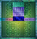
Specifications of NVIDIA's Tesla K20 GPU compute processor, which was launched way back in May, are finally disclosed. We've known since then that the K20 is based on NVIDIA's large GK110 GPU, a chip never used to power a GeForce graphics card, yet. Apparently, NVIDIA is leaving some room on the silicon that allows it to harvest it better. According to a specifications sheet compiled by Heise.de, Tesla K20 will feature 13 SMX units, compared to the 15 available on the GK110 silicon.
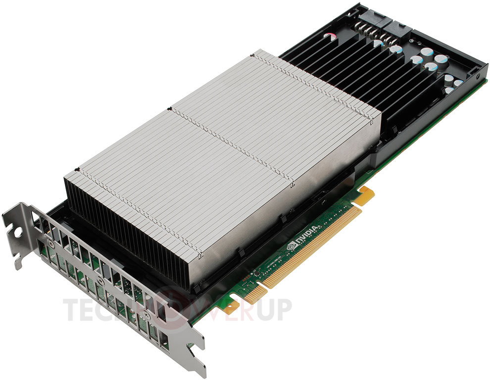
With 13 streaming multiprocessor (SMX) units, the K20 will be configured with 2,496 CUDA cores (as opposed to 2,880 physically present on the chip). The core will be clocked at 705 MHz, yielding single-precision floating point performance of 3.52 TFLOP/s, and double-precision floating point performance of 1.17 TFLOP/s. The card packs 5 GB of GDDR5 memory, with memory bandwidth of 200 GB/s. Dynamic parallelism, Hyper-Q, GPUDirect with RDMA are part of the new feature-set. The TDP of the GPU is rated at 225W, and understandably, it uses a combination of 6-pin and 8-pin PCI-Express power connectors. Built in the 28 nm process, the GK110 packs a whopping 7.1 billion transistors.
Source:
Heise.de
With 13 streaming multiprocessor (SMX) units, the K20 will be configured with 2,496 CUDA cores (as opposed to 2,880 physically present on the chip). The core will be clocked at 705 MHz, yielding single-precision floating point performance of 3.52 TFLOP/s, and double-precision floating point performance of 1.17 TFLOP/s. The card packs 5 GB of GDDR5 memory, with memory bandwidth of 200 GB/s. Dynamic parallelism, Hyper-Q, GPUDirect with RDMA are part of the new feature-set. The TDP of the GPU is rated at 225W, and understandably, it uses a combination of 6-pin and 8-pin PCI-Express power connectors. Built in the 28 nm process, the GK110 packs a whopping 7.1 billion transistors.

29 Comments on Tesla K20 GPU Compute Processor Specifications Released
any insults past this post will result in immediate infractions.
It only took me 1 minute to recognize who ran the site and a couple minutes to read the research paper.
The paper didnt have anything to do with Nvidia rather AMD Radeon HD 7970 and its effeciency in GEMM. What was the purpose in introducing that other then to point out difference in effeciency between Nvidia and AMD. It make it all the worse being presented from a blog/site from a Nvidia employee.
For what other purpose than to show that AMD Radeon HD 7970 runs at 90% and not 100% would that link be relative. If he wanted to make the efficiency he could have choosen a number of article on Mr. Harris site. After all Nvidia is his focus but he delibrately pointed to a AMD specific article from all the vast information on a Nvidia dedecated blog/site from a Nvidia employee.
I stuck to just the DGEMM efficiency so I provide a quote by a research paper done by people who run these server on the company this thread is based on, Nvidia. I didnt go out of my way to try to disparrage this thread by providing information of its competitor.
He just wasnt intrested in providing information but disparraging the competition which does a dis-service to the forum. The evidence is his responce in this quote below..Nothing to do with efficiency in GEMM in anyway. Just baiting.
Thats all...
Just for the record, I was the one that introduced DGEMM as an example. There are numerous other examples of real-world vs theoretical throughput- I chose DGEMM because being open source it favours no vendor