Friday, September 29th 2006

NVIDIA GeForce 8800GTX and GT Pictures


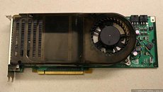
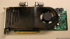
Here's a link to the PC Club forums thread, which shows first pictures of NVIDIA's latest GeForce 8800GTX and GeForce 8800GT video cards, based on the G80 GPU. You can clearly see how massive the new cards are going to be. The one with the water cooling is GeForce 8800GTX, the other is 8800GT version.
Source: PC Club
Add your own comment

41 Comments on NVIDIA GeForce 8800GTX and GT Pictures

#26
POGE
Biggar is bettar right? :p
Posted on Reply
#27
Ketxxx
Heedless Psychic
lol, no. i say ati and nvidia take a seat and work on proper solutions, in the meantime programmers whill just have to *shock, horror* actually program code and optimise it half decently for a change.
Posted on Reply
#28
Ketxxx
Heedless Psychic
i know various programmers. its not the programmers of game engines im critisising, but the developers of games utilising that particular game engine. the game engine itself is already highly optimised, its the code thats based around it that isnt.
Posted on Reply
#29
Canuto
Top end cards are just not worth it!

People look a X1650pro and a X1950XTX have the same image quality the XTX gives you 25% ~ 75% more performance for +100% money and demands tons of juice/power.

We're much better buying a mid range card every year...
Posted on Reply
#30
Ketxxx
Heedless Psychic
logically thats inaccurate. i agree buying the very top end cards are not worth it. however buying a card thats one or two steps down the ladder is worth it. for example, 6800gt over the 6800ultra, or a 7900gt over a 7900gtx.
Posted on Reply
#31
Canuto
Well yeah but i don't consider a 7900Gt to be a top end it's more like a mid/top to me it's price now is about 300€(not sure) and... you got my point 500€ cards are just not worth it.
Posted on Reply
#32
Pheonix_789
I want to see the price and specs of an 8600 GT I hope it will be at least 256Bit
Posted on Reply
#33
SPHERE
img80.imageshack.us/img80/6281/1159518316603in2.jpg

ooo!! i like the look of that mem interface :p damn look at that thing lol the mem chips incircle the core :p it looks like they are 32-bit per chanel too like ati's x1000 line

humm yeah card is a bit long lol but i got long cases so if i end up gettin one shouldnt be a prob :)

a intersting thing i noticed is the soldering point for a bigger pcie power connector.. humm maby that's what they will have on the card in the final version? (pcie 2.0 power connector possibly??)
EastCoasthandleWait, you guys see nothing wrong with 2 PCI express, 6 pin connectors, the "buzzer" at the end of the cards (vista requirement, I'm sure) and the option to have both HSF and what looks like a radiator water cooling solution using alu plating with 90 degree bends??? Come on this thing looks like a pure crap to me. I mean come on, at least offer a brick power supply to offset the dual PSU requirements, sheesh talk about inefficient and backwards.

Here is the possible AGP, SLI version
rofl nice photo shop lol
Posted on Reply
#34
KennyT772
no theres simply a 128bit ram buffer and then 256bit vram. that way games can load next levels textures into the secondary ram and cut loading times ;)
Posted on Reply
#35
SPHERE
KennyT772no theres simply a 128bit ram buffer and then 256bit vram. that way games can load next levels textures into the secondary ram and cut loading times ;)
where did you read this?
Posted on Reply
#36
KennyT772
between the lines

its the most logical answer as the next step for a ram bus would be 512bit. being a 256+128 means master and secondary ram banks. i bet 8 chips are on the 256bit bus and 4 on the 128bit bus. its also most logical to use the 256bit bus for active textures as it has higher performance. its also another logical idea to use the secondary ram bank for prefetching textures and geometry files as that is one major hinderance of todays cards. no game for well over 2 years will be able to fully use 768mb ram on card so nvidia will make some creative use for it.
Posted on Reply
#37
SPHERE
KennyT772between the lines

its the most logical answer as the next step for a ram bus would be 512bit. being a 256+128 means master and secondary ram banks. i bet 8 chips are on the 256bit bus and 4 on the 128bit bus. its also most logical to use the 256bit bus for active textures as it has higher performance. its also another logical idea to use the secondary ram bank for prefetching textures and geometry files as that is one major hinderance of todays cards. no game for well over 2 years will be able to fully use 768mb ram on card so nvidia will make some creative use for it.
na that wouldnt make sence see here is how i see it they now have 768mb 384 bit of mem that they dinamicaly partition off to how ever they want arrange it

its like having 12 hdds in raid 0 dont make 2 raids and limit your options make one and partition it however you want

there are aplications now that can put use to that much mem like 3ds max etc..

the reason for that much mem and it being 384-bit is cause there isn't enough room for more than that bit size and they are using 512mbit chips im shure if they could find the room they would make it 512bit with 256mbit chips but it would require a pcb with a hella lot of layers

btw if you look at the back it seems they are now using 32 bit per chanel mem interfaces instead of 64-bit per chanel like on previous generations which takes more pcb room and also performs better

?:)?
Posted on Reply
#38
KennyT772
dude..its said right on the nvid released specsheet what there are 2 seperate busses.

what in the hell are you talking about with the ram bitsize
Posted on Reply
#39
SPHERE
KennyT772dude..its said right on the nvid released specsheet what there are 2 seperate busses.

what in the hell are you talking about with the ram bitsize
yeah i saw that "128+256" that makes no sence to have 2 banks on a card you dont see systems with one bank for windows and one bank for programs

even if your interpretatin is correct that is dumb cause it would be slower than just using a 384bit bus for both btw in your previous post you talked about how it loaded textures n stuff into this ram buffer you are theoryizing well thats what a texture buffer is and that is what is on your video card right now :)

its worded as 128bit+256 bit cause they are added its just a werid way of describing that is easily misinterpreted kinda like you could describe the new xeon chipsets as being 128+ 128 bit but in reality its a 256 bit bus

when refering to bit size i was talking about the bus width aka 128-bit 256-bit etc

this will be my last post on this topic i just dont feel like debating lol nothing personal i hate internet debates :)
Posted on Reply
#40
Solaris17
Super Dainty Moderator
Ketxxxlol, no. i say ati and nvidia take a seat and work on proper solutions, in the meantime programmers whill just have to *shock, horror* actually program code and optimise it half decently for a change.
or **OMG THRILLER** realease a peice of hardware that has driver support !!!! :eek: :eek: omg i know imagine that?! wow.
Posted on Reply
#41
vexd
technicksCrappy looking.
rofl my video card could literally look like a piece of s**t and i wouldnt care, its what it does that counts ^^
Posted on Reply
Add your own comment
Jan 9th, 2025 15:34 EST change timezone

New Forum Posts

Popular Reviews

Controversial News Posts