Thursday, April 10th 2014

NVIDIA GeForce GTX 880 Detailed
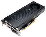
NVIDIA's next-generation GeForce GTX 880 graphics card is shaping up to be a true successor to the GTX 680. According to a Tyden.cz report, GTX 880 will be based on NVIDIA's GM204 silicon, which ranks within its product stack in the same way GK104 does to the GeForce "Kepler" family. It won't be the biggest chip based on the "Maxwell" architecture, but will have what it takes to outperform even the GK110, again, in the same way GK104 outperforms GF110. The DirectX 12-ready chip will feature an SMM (streaming multiprocessor Maxwell) SIMD design that's identical to that of the GeForce GTX 750 Ti, only there are more SMMs, spread across multiple graphics processing clusters (GPCs), probably cushioned by a large slab of cache.This is what the GTX 880 is shaping up to be.
Sources:
PCTuning Tyden.cz, Expreview
- 20 nm GM204 silicon
- 7.9 billion transistors
- 3,200 CUDA cores
- 200 TMUs
- 32 ROPs
- 5.7 TFLOP/s single-precision floating-point throughput
- 256-bit wide GDDR5 memory interface
- 4 GB standard memory amount
- 238 GB/s memory bandwidth
- Clock speeds of 900 MHz core, 950 MHz GPU Boost, 7.40 GHz memory
- 230W board power

102 Comments on NVIDIA GeForce GTX 880 Detailed
Can't hurt to have 8GB on board really. As resolutions increase and textures get bigger to support those resolutions video memory will be paramount.