Tuesday, January 27th 2015

GTX 970 Memory Drama: Plot Thickens, NVIDIA has to Revise Specs
It looks like NVIDIA's first response to the GeForce GTX 970 memory allocation controversy clearly came from engineers who were pulled out of their weekend plans, and hence was too ambiguously technical (even for us). It's only on Monday that NVIDIA PR swung into action, offering a more user-friendly explanation on what the GTX 970 issue is, and how exactly did they carve the GM204 up, when creating the card.
According to an Anandtech report, which cites that easy explanation from NVIDIA, the company was not truthful about specs of GTX 970, at launch. For example, the non-public document NVIDIA gave out to reviewers (which gives them detailed tech-specs), had clearly mentioned ROP count of the GTX 970 to be 64. Reviewers used that count in their reviews. TechPowerUp GPU-Z shows ROP count as reported by the driver, but it has no way of telling just how many of those "enabled" ROPs are "active." The media reviewing the card were hence led to believe that the GTX 970 was carved out by simply disabling three out of sixteen streaming multiprocessors (SMMs), the basic indivisible subunits of the GM204 chip, with no mention of other components like the ROP count, and L2 cache amount being changed from the GTX 980 (a full-fledged implementation of this silicon).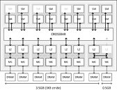
 NVIDIA explained to Anandtech that there was a communication-gap between the engineers (the people who designed the GTX 970 ASIC), and the technical marketing team (the people who write the Reviewer's Guide document, and draw the block-diagram). This team was unaware that with "Maxwell," you could segment components previously thought indivisible, or that you could "partial disable" components.
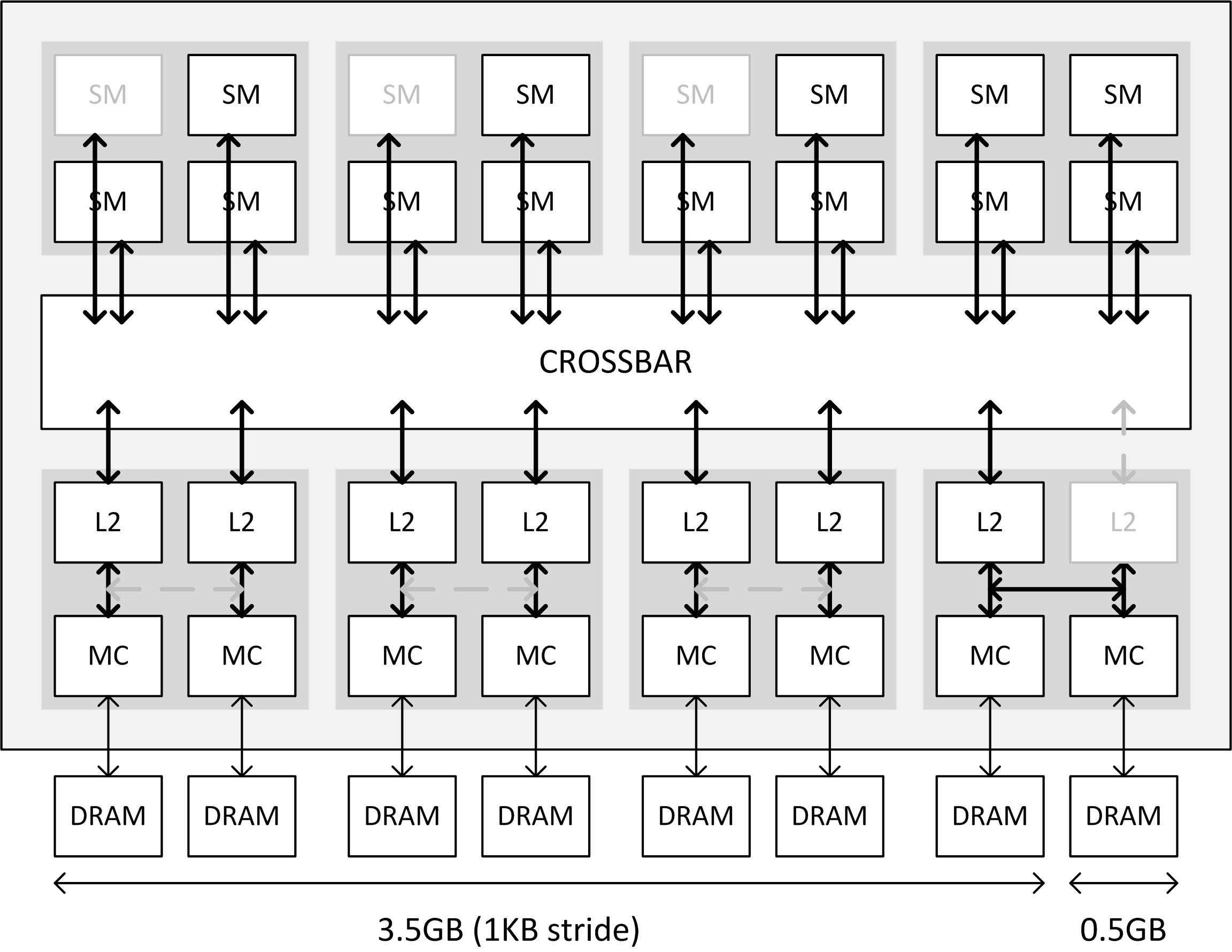
It turns out that in addition to three SMX units being disabled (resulting in 1,664 CUDA cores), NVIDIA reduced the L2 cache (last-level cache) on this chip to 1.75 MB, down from 2 MB, and also disabled a few ROPs. The ROP count is effectively 56, and not 64. The last 8 ROPs aren't "disabled." They're active, but not used, because their connection to the crossbar is too slow (we'll get to that in a bit). The L2 cache is a key component of the "crossbar." Think of the crossbar as a town-square for the GPU, where the various components of the GPU talk to each other by leaving and picking-up data labeled with "from" and "to" addresses. The crossbar routes data between the four Graphics Processing Clusters (GPCs), and the eight memory controllers of 64-bit bus width each (which together make up its 256-bit wide memory interface), and is cushioned by the L2 cache.
The L2 cache itself is segmented, and isn't a monolithic slab of SRAM. Each of the eight memory controllers on the GM204 is ideally tied to its segment of the L2 cache. Also tied to these segments are segments of ROPs. With NVIDIA reducing the L2 cache amount by disabling one such segment. Its component memory controller is instead rerouted to the cache segment of a neighbouring memory controller. Access to the crossbar for that memory controller is hence slower. To make sure there are no issues caused to the interleaving of these memory controllers, adding up to the big memory amount figure that the driver can address, NVIDIA partitioned the 4 GB of memory to two segments. The first is 3.5 GB large, and is made up of memory controllers with access to their own segments of the L2; the second segment is 512 MB in size, and is tied to that memory controller which is rerouted.
The way this partitioning works, is that the 3.5 GB partition can't be read while the 512 MB one is being read. Only to an app that's actively using the entire 4 GB of memory, there will be a drop in performance, because the two segments aren't being read at the same time. The GPU is either addressing the 3.5 GB segment, or the 512 MB one. Hence, there's a drop in performance to be expected, again, for apps that use up the entire 4 GB of memory.
While it's technically correct that the GTX 970 has a 256-bit wide memory interface, and given its 7.00 GHz (GDDR5-effective) memory clock, that translates to 224 GB/s of bandwidth on paper, not all of that memory is uniformly fast. You have 3.5 GB of it having normal access to the crossbar (the town-square of the GPU), and 512 MB of it having slower access. Therefore, the 3.5 GB segment really just has 196 GB/s of memory bandwidth (7.00 GHz x 7 ways to reach the crossbar x 32-bit width per chip), which can be said with certainty. Nor can we say how this segment affects the performance of the memory controller whose crossbar port it's using, if the card is using its full 4 GB. We can't tell how fast the 512 MB second segment really is. But it's impossible for the second segment to make up 28 GB/s (of the 224 GB/s), since NVIDIA itself claims this segment is running slower. Therefore NVIDIA's claims of GTX 970 memory bandwidth being 224 GB/s at reference clocks is inaccurate.
Why NVIDIA chose to reduce cache size and ROP count will remain a mystery. We can't imagine that the people designing the chip will not have sufficiently communicated this to the driver and technical marketing teams. To claim that technical marketing didn't get this the first time around, seems like a hard-sell. We're pretty sure that NVIDIA engineers read reviews, and if they saw "64 ROPs" on a first-page table, they would have reported it up the food-chain at NVIDIA. An explanation about this hardware change should have taken up an entire page in the technical documents the first time around, and NVIDIA could have saved itself a lot of explanation, much of it through the press.
Source:
Anandtech
According to an Anandtech report, which cites that easy explanation from NVIDIA, the company was not truthful about specs of GTX 970, at launch. For example, the non-public document NVIDIA gave out to reviewers (which gives them detailed tech-specs), had clearly mentioned ROP count of the GTX 970 to be 64. Reviewers used that count in their reviews. TechPowerUp GPU-Z shows ROP count as reported by the driver, but it has no way of telling just how many of those "enabled" ROPs are "active." The media reviewing the card were hence led to believe that the GTX 970 was carved out by simply disabling three out of sixteen streaming multiprocessors (SMMs), the basic indivisible subunits of the GM204 chip, with no mention of other components like the ROP count, and L2 cache amount being changed from the GTX 980 (a full-fledged implementation of this silicon).

It turns out that in addition to three SMX units being disabled (resulting in 1,664 CUDA cores), NVIDIA reduced the L2 cache (last-level cache) on this chip to 1.75 MB, down from 2 MB, and also disabled a few ROPs. The ROP count is effectively 56, and not 64. The last 8 ROPs aren't "disabled." They're active, but not used, because their connection to the crossbar is too slow (we'll get to that in a bit). The L2 cache is a key component of the "crossbar." Think of the crossbar as a town-square for the GPU, where the various components of the GPU talk to each other by leaving and picking-up data labeled with "from" and "to" addresses. The crossbar routes data between the four Graphics Processing Clusters (GPCs), and the eight memory controllers of 64-bit bus width each (which together make up its 256-bit wide memory interface), and is cushioned by the L2 cache.
The L2 cache itself is segmented, and isn't a monolithic slab of SRAM. Each of the eight memory controllers on the GM204 is ideally tied to its segment of the L2 cache. Also tied to these segments are segments of ROPs. With NVIDIA reducing the L2 cache amount by disabling one such segment. Its component memory controller is instead rerouted to the cache segment of a neighbouring memory controller. Access to the crossbar for that memory controller is hence slower. To make sure there are no issues caused to the interleaving of these memory controllers, adding up to the big memory amount figure that the driver can address, NVIDIA partitioned the 4 GB of memory to two segments. The first is 3.5 GB large, and is made up of memory controllers with access to their own segments of the L2; the second segment is 512 MB in size, and is tied to that memory controller which is rerouted.
The way this partitioning works, is that the 3.5 GB partition can't be read while the 512 MB one is being read. Only to an app that's actively using the entire 4 GB of memory, there will be a drop in performance, because the two segments aren't being read at the same time. The GPU is either addressing the 3.5 GB segment, or the 512 MB one. Hence, there's a drop in performance to be expected, again, for apps that use up the entire 4 GB of memory.
While it's technically correct that the GTX 970 has a 256-bit wide memory interface, and given its 7.00 GHz (GDDR5-effective) memory clock, that translates to 224 GB/s of bandwidth on paper, not all of that memory is uniformly fast. You have 3.5 GB of it having normal access to the crossbar (the town-square of the GPU), and 512 MB of it having slower access. Therefore, the 3.5 GB segment really just has 196 GB/s of memory bandwidth (7.00 GHz x 7 ways to reach the crossbar x 32-bit width per chip), which can be said with certainty. Nor can we say how this segment affects the performance of the memory controller whose crossbar port it's using, if the card is using its full 4 GB. We can't tell how fast the 512 MB second segment really is. But it's impossible for the second segment to make up 28 GB/s (of the 224 GB/s), since NVIDIA itself claims this segment is running slower. Therefore NVIDIA's claims of GTX 970 memory bandwidth being 224 GB/s at reference clocks is inaccurate.
Why NVIDIA chose to reduce cache size and ROP count will remain a mystery. We can't imagine that the people designing the chip will not have sufficiently communicated this to the driver and technical marketing teams. To claim that technical marketing didn't get this the first time around, seems like a hard-sell. We're pretty sure that NVIDIA engineers read reviews, and if they saw "64 ROPs" on a first-page table, they would have reported it up the food-chain at NVIDIA. An explanation about this hardware change should have taken up an entire page in the technical documents the first time around, and NVIDIA could have saved itself a lot of explanation, much of it through the press.
138 Comments on GTX 970 Memory Drama: Plot Thickens, NVIDIA has to Revise Specs
Refund calcs (from previous thread)... 3.5 vs 4.0, I say a 13% refund, lol
The engineers probably had a lot of 980s with bad yields at production and they just lasercut them to 970s. It has been a practice for many generations and they never lied about it before why would they start it now? Seriously why?
On a classic motherboard... without some revolution ie proprietary connector to the motherboard nope...
Kinda stumped on what to do next tbh. Might try to return these 2 970s and pick up to 780Ti's off ebay or something on the cheap.
I saw this in downtown Providence and snapped a photo, he should start a video card ad campaign.
And 4K on 970? Where is the problem for older games? All UT3 games? Grid2? Civ? Source based games? And millions of users still for WoW?
If Intel could get away with the TSX errata found on Haswell CPUs (feature removed through microcode update after the bug was discovered by the community), I can't see why NV will not considering the performance of GTX970 hasn't changed a bit before or after this marketing fiasco.
I've worked in a few large corporations and marketing tends to live in their own little world of schmoozing and BS. But they wouldn't be allowed mod the specs without the consent of the top brass. The tech guys would likely have had no say in the matter at all.
The big question in my mind is... did everyone involved expect this scenario to play out like it is, or were they really dumb enough to think no one would notice? The ROPs and cache thing is really weird, because nobody would give a damn about those specs on their own. It's the gimped vram that is bothersome. Maybe they were thinking that would tip someone off that the architecture was funny and prompt them to investigate further? And they wanted the 970 to have a few months of "honeymoon" where it sold like crazy and forced AMD to slash prices on their 290 and 290x. Then they'd do the inevitable dance and damage control later.
I don't know... what would have happened if Nvidia had told everyone it was 3.5GB+ at the start? I can see marketing's point of view... you don't want to present your new hot product and put "gimped architecture weirdness" in everyone's mind. It definitely gives it one issue that makes it inferior to the competing AMD products, which have 4GB of vram. I'm certain it would have hurt sales and tainted reviews. But it's also hard to imagine that they'd prefer what is happening now. The 970 is still early in it's life cycle and if Nvidia compensates customers, that will certainly cost them more $ than if they were honest at the start.
Doesn't anybody know some one who works there and can tell us what's really going on?
Nvidia over priced GTX980 by publishing false GTX970 spec so that it appears to be close to GTX980 specs to justify the price they put on the GTX980.
If the real specs for the GTX970 were known from the start i bet the GTX980 would not be selling at those high prices it would be more of around $399 ish to justify the small performance gain it has over the GTX970
In the future if someone running this card runs into a game that uses 4gb of memory and it runs slower because its using all 4gb of memory thats an issue, and issue that should have been clearly explained by Nvidia.
The fact is people bought a card that advertized 4gb of available vram, not a card with 3.5gb of vram and the possibility to use 4gb at reduced performance.
Quote from Transformers (2007):
00:18:53,432 --> 00:18:56,458
Wow. You are so cheap.
As for older games on 4K, I do not think it is going to be a problem. Quite the contrary, it will be a great experience, and a single GTX 970 should suffice, if not more than suffice. But from what I have read some people bought a single GTX 970 and expected to run games like Assassin's Creed: Unity and even Dragon Age: Inquisition on 4K resolution. SLI setup, perhaps. But a single card?
And I apologise if my English is not fluent and understandable. I tried not to use a machine translator. Hopefully nobody would get confused by my poor choice of words.
They didn't lie about ROP count. The card has 64 Active ROPs. That is not a lie. It only uses 56 of them because using the others would actually slow the card down. But there are 64 active ROPs.
They didn't lie about memory amount, it has 4GB and all 4GB can be accessed if needed. The last 0.5GB is slower than the first 3.5GB, but so what? It is still faster than accessing system RAM. If they had designed the card as a strict 224-Bit 3.5GB card, it would have been slower than the 970 we got. There is no getting around that. They made the decisions they did with the extra 0.5GB because it improves the performance of the card.
Yeah, there is some marketing slight of hand going on here. But the fact is the card performs great, even at 4k.
Personally, I think they could have left all the specs the listed the same(except L2 size, but again I wouldn't even have listed that). But they should have given this explanation to the reviewers from the beginning, so they could include in their reviews how the memory subsystem works from the beginning.
I'm guessing they really thought no one would notice, or at least not until later this year.
"Active" matters little here. That's like super gluing a turbo charger on to the hood of a car and selling it as "turbo charged" when it is not. If the hardware is there but deliberately designed to not be used, it shouldn't be advertised as being there.
Choose R9 290 Series for its uncompromised 4GB memory: AMD
:laugh::laugh::laugh::laugh: