Thursday, February 2nd 2017

MSI M.2 Shield is Snake Oil Say Tests, Company Refutes Charges

With its 200-series chipset motherboards, MSI introduced its exclusive M.2 Shield accessory on some of its more premium products. This aluminium heatspreader with a thermal pad, according to its makers, is designed to lower temperatures on M.2 SSDs, and reduce thermal throttling of performance. Tests by Gamers Nexus claim that far from reducing throttling, the M.2 Shield creates a "heat trap" that throttles performance further.

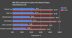
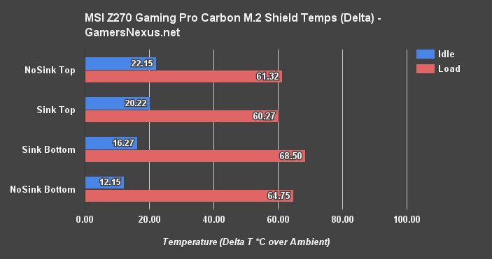
The M.2 Shield accessory was tested by Gamers Nexus using a Kingston HyperX Predator PCIe M.2 drive, on an MSI Z270 Gaming Pro Carbon motherboard. Driven by a Marvell 88SS9293 controller, the drive is known to heat up and lose performance to overheating. The data presented by the publication is Delta T (temperatures subtracting ambient temperature). MSI on its part, stands by the efficacy of the M.2 Shield accessory, and is sharing testing methods and data of its own with media sites. Tests by other publications such as Bit-Tech and KitGuru show positive results for the M.2 Shield.
Sources: GamersNexus, ComputerBase.de
Add your own comment

38 Comments on MSI M.2 Shield is Snake Oil Say Tests, Company Refutes Charges

#26
VSG
Editor, Reviews & News
SteevoI'm not trying to be an asshole, I work with precision GPS for a living, and understand the difference in quality. Sometimes trying to explain why an oscilloscope is needed to diagnose a problem to an average tech spills over here.
Oh you are not being an asshole at all, I really appreciate the discussion- we have no vested interest here except to learn more so I am all for it.
Posted on Reply
#27
newtekie1
Semi-Retired Folder
Here is my take on the whole thing. If the heat issues of M.2 drives could be fixed with a simple heat spreader, the M.2 manufacturers would have added heat spreaders to their drives a long time ago. I refuse to believe none of them thought about trying that to see if it helped. So, since they don't come with heatspreaders, I'd be willing to bet that the MSI heatspreader isn't really helping any.

It looks cool though...
Posted on Reply
#28
Steevo
newtekie1Here is my take on the whole thing. If the heat issues of M.2 drives could be fixed with a simple heat spreader, the M.2 manufacturers would have added heat spreaders to their drives a long time ago. I refuse to believe none of them thought about trying that to see if it helped. So, since they don't come with heatspreaders, I'd be willing to bet that the MSI heatspreader isn't really helping any.

It looks cool though...
Reviewers have listed 4W as the power consumption of high end drives, it may be higher than that however especially as temperature increases. I'm sure most don't come with anything to meet size specifications, and much like older GDDR it probably isn't the memory but the controller that is producing most of the heat and that has to be kept at a lower temp. Drive watercoolers may finally have a use.
Posted on Reply
#29
VSG
Editor, Reviews & News
Yup, the controllers on the M.2 SSDs are the heat issue. The flash modules themselves are fine. As someone else pointed out, Aquacomputer has a watercooled M.2 adapter if you have a custom loop already.
Posted on Reply
#30
MaMoo
VSGMy point when I brought this up was that I do not trust thermal imaging as a means of quantifying heat, and so I am taking the Toms Hardware numbers with a grain of salt. The exact VRM modules used on those cards are rated at well above 125 °C, including the ones that went bad. Gamers Nexus used multiple thermocouples with EMI shieldingand showed that temps were well within rated specs with and without the new BIOS and thermal pad kit. To bring this back to topic, I argue the same applies to the M.2 heatsink test here- thermal imaging done by Kitguru is not something I agree with, so I am more reliant to take the Gamers Nexus tests as a point of reference.

That said, I did note some things that need to be re-done and I have been having discussions with Steve about this since Monday. So that Gamers Nexus article will be updated shortly. Similarly, I can definitely understand the skepticism behind the EVGA VRM issue and I wholeheartedly agree that the issue was not resolved to my satisfaction either. My contacts at EVGA mentioned it may have been bad modules, but without the actual data it is left to their word.
There are two things I find suspect with the thermocouple and 125 °C ideas. The first is that thermocouples are typically used to probe larger objects and coupling is always an issue with smaller objects. In Gamers Nexus's final tests, the thermal couple was coupled to the back of the PCB. This can only measure the stead-state temperature of the back side. To extrapolate that number to actual VRM temperatures, one would have to assume a steady-state thermal gradient and do a few multiplications. One way to obtain that, would be the use of a thermal imaging device.

Which brings us to our second issue, these VRM packages are like any other silicon chip - the core is much hotter than the plastic packaging since the heat is generated in the silicon parts underneath. The manufacturer of the VRM chips usually assumes a given amount of cooling and hence an expected thermal gradient range, which is why the VRM as a whole package is specified for Tcase temperatures, when really, the MOSFETs are the main sources of heat. It is up to the GPU maker to implement such a thermal gradient. Given this thermal gradient, it is not clear what the core temperature of these VRM chips are. This is further complicated due to the power MOSFETs in the VRMs being typically specified for a steady-state thermal impedance and a transient thermal impedance (and in general the whole package features this distinction as well, due to thermal capacitance of any finite-sized object). A small burst workload (<1 second) close enough to the maximal internal channel temperatures at already high duty may trigger a transient over-temperature condition (in the silicon parts and not measurable as steady-state increases of temperature outside the package) and cause eventual failure through aggregated damage if not immediate.

For the longevity and reliability of these VRM chips, I would think a good design would be to keep the MOSFETs several 10s of degrees below the 125°C maximum to ensure actual MOSFET channel temperatures are always below the maximal channel temperatures specified. To do so, you would need to ensure the thermal gradient across the VRM chips to be as low as possible, which means effective cooling coupling in the form of a heatsink (that lowers the thermal impedance of the VRMs to the surrounding air).
Posted on Reply
#31
FordGT90Concept
"I go fast!1!11!1!"
Kind of disappointed they didn't test the EMI aspects of it. EMI is the only reason why I could see using it. That said, is there even any documented evidence that EMI shielding on an SSD would either prolong the life of the SSD or decrease the error rate? I doubt it. Still...due diligence...
Posted on Reply
#32
Steevo
Maxx_PowerThere are two things I find suspect with the thermocouple and 125 °C ideas. The first is that thermocouples are typically used to probe larger objects and coupling is always an issue with smaller objects. In Gamers Nexus's final tests, the thermal couple was coupled to the back of the PCB. This can only measure the stead-state temperature of the back side. To extrapolate that number to actual VRM temperatures, one would have to assume a steady-state thermal gradient and do a few multiplications. One way to obtain that, would be the use of a thermal imaging device.

Which brings us to our second issue, these VRM packages are like any other silicon chip - the core is much hotter than the plastic packaging since the heat is generated in the silicon parts underneath. The manufacturer of the VRM chips usually assumes a given amount of cooling and hence an expected thermal gradient range, which is why the VRM as a whole package is specified for Tcase temperatures, when really, the MOSFETs are the main sources of heat. It is up to the GPU maker to implement such a thermal gradient. Given this thermal gradient, it is not clear what the core temperature of these VRM chips are. This is further complicated due to the power MOSFETs in the VRMs being typically specified for a steady-state thermal impedance and a transient thermal impedance (and in general the whole package features this distinction as well, due to thermal capacitance of any finite-sized object). A small burst workload (<1 second) close enough to the maximal internal channel temperatures at already high duty may trigger a transient over-temperature condition (in the silicon parts and not measurable as steady-state increases of temperature outside the package) and cause eventual failure through aggregated damage if not immediate.

For the longevity and reliability of these VRM chips, I would think a good design would be to keep the MOSFETs several 10s of degrees below the 125°C maximum to ensure actual MOSFET channel temperatures are always below the maximal channel temperatures specified. To do so, you would need to ensure the thermal gradient across the VRM chips to be as low as possible, which means effective cooling coupling in the form of a heatsink (that lowers the thermal impedance of the VRMs to the surrounding air).
They can calculate the expected TDP of any VRM with a few simple tests, gate cross-section, voltage and resistance on the load side, plus capacitive and inductive losses (these go way up as temperature increases). The more I look at the failures the more it looks like the solder is getting too hot and it melts enough to short out but still has high enough resistance the PSU doesn't cut off before it kills the GPU and everything close to the VRM. The voltage controller in PLL mode should be driving them all the same and is able to calculate the approximate wattage through the VRM's in milliseconds so the VRM's being overdriven/overloaded shouldn't be an issue unless the solder points were high resistance.
Posted on Reply
#34
hapkiman
DimiI have no idea what this title means. Anyone care to explain?
Seriously - you don't know what "snake oil" is?

It means it's a fugazzi.
Posted on Reply
#35
MaMoo
SteevoThey can calculate the expected TDP of any VRM with a few simple tests, gate cross-section, voltage and resistance on the load side, plus capacitive and inductive losses (these go way up as temperature increases). The more I look at the failures the more it looks like the solder is getting too hot and it melts enough to short out but still has high enough resistance the PSU doesn't cut off before it kills the GPU and everything close to the VRM. The voltage controller in PLL mode should be driving them all the same and is able to calculate the approximate wattage through the VRM's in milliseconds so the VRM's being overdriven/overloaded shouldn't be an issue unless the solder points were high resistance.
Interesting hypothesis. I think that the lack of direct feedback at the driver about the instantaneous thermal condition of the MOSFETs had some role. Given that the external temperatures of the VRMs were close enough to the maximum rated case temperatures, I wouldn't be surprised if the channel temperatures occasionally exceeded safe channel temperatures. The poor solder contact through melting (I'm not sure what solder they used, whether it is eutectic or some other formulation) would reduce heat transfer substantially to the PCB, which in the absence of a proper heatsink, is the best source of cooling (usually spread through a couple of vias or a large ground plane on the PCB). Typically without something like a PowerPAD on the top side, the solder side of the VRM packages is the hottest side.

Anyway, we do not have any means to figure this out completely. I do think there are issues with the tests conducted with thermal probes.
Posted on Reply
#36
KarymidoN
DimiI have no idea what this title means. Anyone care to explain?
URBAN DICTIONARYcomes from the 19th-century American practice of selling cure-all elixirs in traveling medicine shows. Snake oil salesmen would falsely claim that the potions would cure any ailments. Now-a-days it refers to fake products.
Posted on Reply
#37
Gasaraki
Sorry the Gamer Nexus test is flawed. They actually said that it lower the temperature of the SSD but the back of the SSD got hotter.

1-Most SSDs don't have chips on the back or not a lot of chips.
2-The back of the SSD will be the same with or without the shield, the shield only covers the front surface so how is the shield blocking the back at all.
Posted on Reply
#38
Ruru
S.T.A.R.S.
GasarakiSorry the Gamer Nexus test is flawed. They actually said that it lower the temperature of the SSD but the back of the SSD got hotter.

1-Most SSDs don't have chips on the back or not a lot of chips.
2-The back of the SSD will be the same with or without the shield, the shield only covers the front surface so how is the shield blocking the back at all.
My Intel 600p 256GB has chips only on one side, I have Alphacool's heatspreader on it and depending on the situation, it runs 5-10C cooler.
Posted on Reply
Add your own comment
Feb 16th, 2025 08:11 EST change timezone

Popular Reviews

Controversial News Posts