Friday, September 8th 2017

AMD To Change Suppliers for Vega 20 GPUs on 7nm, HBM2 Packaging for Vega 11
AMD's RX Vega supply has seen exceedingly limited quantities available since launch. This has been due to a number of reasons, though the two foremost that have been reported are: increased demand from cryptocurrency miners, who are looking towards maximizing their single node hashrate density through Vega's promising mining capabilities; and yield issues with AMD's Vega 10 HBM2 packaging partner, Advanced Semiconductor Engineering (ASE). It's expected that chip yield for Vega 10 is also lower per se, due to it having a 484 mm² die, which is more prone to defects than a smaller one, thus reducing the amount of fully-enabled GPUs.
AMD's production partner, GlobalFoundries, has historically been at the center of considerations on AMD's yield problems. That GlobalFoundries is seemingly doing a good job with Ryzen may not be much to say: those chips have incredibly small die sizes (192 mm²) for their number of cores. It seems that Global Foundries only hits problems with increased die sizes and complexity (which is, unfortunately for AMD, where it matters most).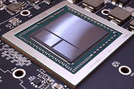
 Due to these factors, it seems that AMD is looking to change manufacturers for both their chip yield issues, and packaging yield problems. ASE, which has seen a 10% revenue increase for the month of August (not coincidentally, the month that has seen AMD's RX Vega release) is reportedly being put in charge of a much smaller number of packaging orders, with Siliconware Precision Industries (SPIL), who has already taken on some Vega 10 packaging orders of its own, being the one to receive the bulk of Vega 11 orders. Vega 11 is expected to be the mainstream version of the Vega architecture, replacing Polaris' RX 500 series. Reports peg Vega 11 as also including HBM2 memory in their design instead of GDDR5 memory. Considering AMD's HBM memory history with both the original Fury and and now RX Vega, as well as the much increased cost of HBM2's implementation versus a more conventional GDDR memory subsystem, this editor reserves itself the right to be extremely skeptical that this is true. If it's indeed true, and Vega 11 indeed does introduce HBM2 memory to the mainstream GPU market, then... We'll talk when (if) we get there.
As to its die yield issues, AMD is reported to be changing their main supplier for their 7 nm AI-geared Vega 20 from GlobalFoundries to Taiwan Semiconductor Manufacturing Company (TSMC), who has already secured orders for AI chips from NVIDIA and Google. TSMC's 7nm and CoWoS (chip-on-wafer-on-substrate) capabilities have apparently proven themselves enough for AMD to change manufacturers. How this will affect AMD and GlobalFoundries' Wafer Agreement remains to be seen, but we expect AMD will be letting go of some additional payments GlobalFoundries' way.
Sources:
DigiTimes on Vega 11, DigiTimes ASE, DigiTimes on vega Shortages
AMD's production partner, GlobalFoundries, has historically been at the center of considerations on AMD's yield problems. That GlobalFoundries is seemingly doing a good job with Ryzen may not be much to say: those chips have incredibly small die sizes (192 mm²) for their number of cores. It seems that Global Foundries only hits problems with increased die sizes and complexity (which is, unfortunately for AMD, where it matters most).

As to its die yield issues, AMD is reported to be changing their main supplier for their 7 nm AI-geared Vega 20 from GlobalFoundries to Taiwan Semiconductor Manufacturing Company (TSMC), who has already secured orders for AI chips from NVIDIA and Google. TSMC's 7nm and CoWoS (chip-on-wafer-on-substrate) capabilities have apparently proven themselves enough for AMD to change manufacturers. How this will affect AMD and GlobalFoundries' Wafer Agreement remains to be seen, but we expect AMD will be letting go of some additional payments GlobalFoundries' way.
62 Comments on AMD To Change Suppliers for Vega 20 GPUs on 7nm, HBM2 Packaging for Vega 11
I only wanted to know where Global Foundry held their facilities. Not TSMC. This was what cadaveca mistook and we already cleared it up. I hope I've cleared things up here further. :)
But yeah, there's a plethora of things the gaming market brings that it seems stupid to ignore it. Gamers have brand loyalties and future purchases.. not necessarily miners. And working with devs is the other thing. As well as tie in products that miners would never be interested in, like Freesync. Or peripherals.
But fast money has a way of blinding people. And they already got beat down by Intel/Nvidia once.
2. Ryzen die (Zeppelin) is 213 mm2.
3. Vega 11 with HBM is fake news. The original source said it's going to be packaged at the same company as the one that does Vega 10 packages. That's it! Putting a GPU chip on a PCB substrate it's also called "packaging".
All I want to add is that this whole thing is a speculation based on speculation with a speculation on its tail.
1) Manufacturing chips and packaging is not the same thing
2) GN did a little research based on Vega samples and they came to conclusion that there are at least three packaging partners based on major differences in spacing/filling between GPU and HBM
3) Regardless of how much you want to blame miners, they are still on the same boat with everyone else - there is no vega on the market.
Another thing I can't wrap my head around is the contents of the "source" articles.
First one only mentions that SPIL will keep the contract on packaging (theoretically they are one of those three that package Vega10 right now), which may or may not include future 2.5D/3D stacking (putting HBM on top of GPU or vice versa).
Secon one is about ASE revenues and not a word or a hint about which way their partnership with AMD goes.
Third one is about shortages and possible reasons behind it (e.g. HMB supply, packaging yields etc, but not a word about mining).
Lastly, when will you forget that bullshit from twitter about a claim of 43MH/s at 130W. It was already debunked by... I'm gonna say it with a bit of pride and respect this time.... WCFTech and recreated by a dozen people on youtube (averaging at 175W-185W @ 43.5MH/s).
-- Supplies - It delayed the RX Vega launch by three months. How can they get enough for even more products?
-- Assembly issues
Do you see any Vega 10 in there?
The products are called RX Vega 64, RX Vega 56, Vega Frontier Edition, etc.
You can blame AMD for the confusion here.
Edit: See community.amd.com/thread/218613
Both Vega 64 and 56 are Vega 10 , Vega 11 does not exist yet. I think this is a case of people just simply not paying enough attention , things have been clear as daylight.
Both AMD and Nvidia are often manufacturing a single GPU and releasing different variants based on it. This has been happening for ages but for some reason now it sparks confusion.
I give up.
I guess you have to be this geek or nerd or whatever thing to understand this shit. I have better things to do in my life than memorizing cryptic and confusing hardware names.
Vega 11 is a future Polaris replacement w/ 6144 shader units at the top.
Vega 20 is an even "futurer" replacement-replacement to Vega 10.
This is AMD's fault too, mostly for announcing a shitton of stuff simultaneously ahead of time with some over-optimistic time tables. If you've given up on keeping up with
KardashiansVega a few month ago, you expect Vega 10 to be already out and Vega 11 also being almost available or very near release date. Hence the confusion. I'm personally only familiar with some Vega news only thanks to too much free time, outrageous headlines on the internet, and my follow-up tantrums about it.