Friday, June 29th 2018

Intel 10 nm Process Increases Transistor Density by 2.7x Over 14 nm: Report
Intel's 10 nanometer FinFET silicon fabrication is coming together at a slower than expected rate, however when it does, it could vastly enlarge the canvas for the company's chip designers, according to a technical report by Tech Insights. The researchers removed the die of an Intel "Cannon Lake" Core i3-8121U processor inside a Lenovo Ideapad330, and put it under their electron microscope.
Its summary mentions quite a few juicy details of the 10 nm process. The biggest of these is the achievement of a 2.7-times increase in transistor density over the current 14 nm node, enabling Intel to cram up to 100.8 million transistors per square millimeter. A 127 mm² die with nothing but a sea of transistors, could have 12.8 billion transistors. Intel 10 nm node also utilizes third-generation FinFET technology, with a reduction in minimum gate pitch from 70 nm to 54 nm; and minimum metal pitch from 52 nm to 36 nm. 10 nm also sees Intel introduce metallization of cobalt in the bulk and anchor layers of the silicon substrate. Cobalt emerged as a good alternative to tungsten and copper as a contact material between layers, due to its lower resistance at smaller sizes,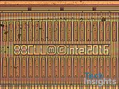


Source:
Tech Insights
Its summary mentions quite a few juicy details of the 10 nm process. The biggest of these is the achievement of a 2.7-times increase in transistor density over the current 14 nm node, enabling Intel to cram up to 100.8 million transistors per square millimeter. A 127 mm² die with nothing but a sea of transistors, could have 12.8 billion transistors. Intel 10 nm node also utilizes third-generation FinFET technology, with a reduction in minimum gate pitch from 70 nm to 54 nm; and minimum metal pitch from 52 nm to 36 nm. 10 nm also sees Intel introduce metallization of cobalt in the bulk and anchor layers of the silicon substrate. Cobalt emerged as a good alternative to tungsten and copper as a contact material between layers, due to its lower resistance at smaller sizes,


28 Comments on Intel 10 nm Process Increases Transistor Density by 2.7x Over 14 nm: Report
spectrum.ieee.org/nanoclast/semiconductors/processors/intel-now-packs-100-million-transistors-in-each-square-millimeter
I wonder if Intel PR orchestrates continued 10 nm "news" leaks, to create an illusion of forward motion.
Tech Insights has gotten their hands on i3-8121U and have been analyzing that.