Sunday, May 28th 2023

New Generation of AMD Threadripper "Storm Peak" Mentioned on CPU-Z
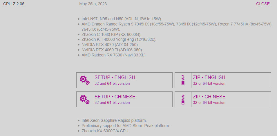
CPUID recently released version 2.06 of the globally popular free CPU-Z utility which includes updates to support reporting of a variety of recent or obscure CPU and GPU models. Intel's "Alder Lake-N", AMD's recently released "Dragon Range" mobile Zen 4 processors, Zhoaxin's KH-40000 and KX-6000G, and of course NVIDIA's RTX 4060 Ti as well as AMD's RX 7600. Most interesting of all is a small addition down at the very bottom of the list, "Preliminary support for AMD Storm Peak platform." "Storm Peak" is AMD's yet to be announced Ryzen Threadripper 7000 series which will feature "Zen 4" and hopefully heat up competition in the HEDT market. No detailed specifications or information on SKUs have been released yet with "Storm Peak" expected to receive a proper announcement sometime in Q3 2023. The mention on CPU-Z suggests that the platform is nearing market readiness, and possibly that the folks at CPUID have been seeded samples or specifications to prepare with. Threadripper 7000 is expected to be released on yet another new socket, TR5, and has been rumored to be coming in both HEDT and workstation variants.
Intel brought competition to the HEDT market for the first time in nearly 4 years with the release of their Sapphire Rapids Xeon W range of processors back in February. Xeon W features unlocked SKUs tackling AMD's Threadripper 5000 series from top to bottom; going as high as the 56-core Xeon w9-3495X at a blistering $5,889 USD to as low as ~$1,000 USD for the 12-core Xeon w5-2455X. Intel also interspersed some lower cost locked SKUs to allow system integrators to offer the new platform as workstations to the prosumer market that generally cares little about overclocking. With Intel competing directly with Threadripper again it was expected that it wouldn't be long before AMD would be cooking up a response with their latest and greatest.

Sources:
HotHardware, CPUID
Intel brought competition to the HEDT market for the first time in nearly 4 years with the release of their Sapphire Rapids Xeon W range of processors back in February. Xeon W features unlocked SKUs tackling AMD's Threadripper 5000 series from top to bottom; going as high as the 56-core Xeon w9-3495X at a blistering $5,889 USD to as low as ~$1,000 USD for the 12-core Xeon w5-2455X. Intel also interspersed some lower cost locked SKUs to allow system integrators to offer the new platform as workstations to the prosumer market that generally cares little about overclocking. With Intel competing directly with Threadripper again it was expected that it wouldn't be long before AMD would be cooking up a response with their latest and greatest.

30 Comments on New Generation of AMD Threadripper "Storm Peak" Mentioned on CPU-Z
sWRX80 socket has eight memory controller DDR4 scaling.
Sapphire Rapids LGA 4677 has PCI 5.0 and DDR5 implementation and eight memory controller DDR5 scaling. The predecessor LGA 4189 (DDR4 and PCI 4.0 implementation) is not compatible with LGA 4677. en.wikipedia.org/wiki/Ice_Lake_(microprocessor)
LGA 7529 is the sucessor to LGA 4677. [URL]https://en.wikipedia.org/wiki/LGA_7529[/URL]
PCIe lane scales according to market segmentation.PCIe version's implementation can occur on SoC's North Bridge and South Bridge chipsets.AMD's IO chip is just the North Bridge.
There is no chipset on the SP3 socket server boards Which use basically the same socket. If the SP3 boards have a chipset, it's one for minor video output. You can go look on newegg, If you don't believe me. The only reason WRX80 has a chipset for is SATA ports mostly & usb c/3.0/2.0 ports. The WRX80 & TRX40 board don't even have HD Audio chips on them. You have to buy a sound card for HD Audio. a few WRX80 boards also have the ability to basic video too.
From www.tomshardware.com/reviews/ryzen-9-3900x-7-3700x-review,6214-2.html
The actual X570 chipset is a 14nm variant of the 12nm I/O die inside the Ryzen 3000-series processors, which is a clever reuse of the technology that ultimately lowers costs.
AMD's products are built-on common building Intellectual property (IP) blocks.
AMD's "I/O die" is the Northbridge which includes a PCIe and memory controller implementation. AMD's "I/O die" Intellectual property (IP) blocks can be recycled for other copy-and-paste engineered Southbridge PCIe-based chips.
The PCB electronic circuit requirements for Southbridge PCIe 4.0 implementation are the same as "I/O die" Northbridge's PCIe 4.0 implementation.
My argument is at the PCIe electrical implementation on per lane basis.
Zen 2 / Zen 3-era PCIe 4.0 / DDR4 implementation is different from Zen 4-era PCIe 5.0 / DDR5 implementation. You're not going to get Zen 4 on a legacy PCIe 4.0 / DDR4-based PCB board design.
AM4 didn't require major memory controller changes e.g. additional memory controllers and a switch from DDR3 to DDR4.
If there's a requirement for the 256-bit bus for mainstream desktop PCs, then AM5 change will need to be changed.SP3 SoC has a built-in chipset i.e. AMD's PCIe-based "I/O die" Northbridge on the chip package.
PCB electronic circuit requirements for SATA and HD Audio are low-end.
I wouldn't really call the I/O die a chipset itself. Since certain AM4 board that can do 8x first slot /8x second slot, They Still have a Pci-express hub switch (which cause latency & stuttering) to just split up the lanes from coming from the cpu. The major of AM4 board though will do 16x first slot/4x second slot, without the hub switch. Those lanes don't even take up the M.2 Nvme lanes usually. Severs general just us the U.2 connection which uses some of the pci-express lanes.
-------
Gigabyte X570 UD's single PCIe 16X slot (PCIEX16) can still split with the mentioned PCIe 8X/ 8X riser card and a BIOS setting.
The rest of the PCIe slots are from the X570 chipset i.e. two PCI Express x16 slots supporting PCIe 4.0/3.0 running at X4 and two PCI Express x1 slots, supporting PCIe 4.0 / 3.0.