Report an Error


NVIDIA GK208

GK208

GK208-301-A1
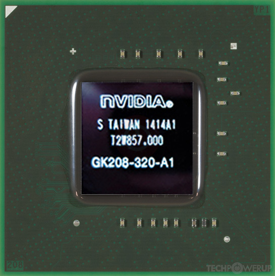
GK208-320-A1

GK208-400-A1

Block Diagram

SMX Diagram
NVIDIA's GK208 GPU uses the Kepler 2.0 architecture and is made using a 28 nm production process at TSMC. With a die size of 87 mm² and a transistor count of 1,020 million it is a very small chip. GK208 supports DirectX 12 (Feature Level 11_0). For GPU compute applications, OpenCL version 3.0 and CUDA 3.5 can be used. It features 384 shading units, 32 texture mapping units and 8 ROPs.
Graphics Processor
- Released
- Apr 1st, 2013
- GPU Name
- GK208
- Codename
- NV108
- Architecture
- Kepler 2.0
- Foundry
- TSMC
- Process Size
- 28 nm
- Transistors
- 1,020 million
- Density
- 11.7M / mm²
- Die Size
- 87 mm²
- Package
- FCBGA-595
Graphics Features
- DirectX
- 12 (11_0)
- OpenGL
- 4.6
- OpenCL
- 3.0
- Vulkan
- 1.2.175
- CUDA
- 3.5
- Shader Model
- 6.5 (5.1)
- WDDM
- 3.0
- NVENC
- No Support
- NVDEC
- 1st Gen
- PureVideo HD
- VP5
- VDPAU
- Feature Set D
Render Config
- Shading Units
- 384
- TMUs
- 32
- ROPs
- 8
- SMX Count
- 2
- GPCs
- 1
- Tex L1 Cache
- 48 KB per SMX
- L1 Cache
- 16 KB per SMX
- L2 Cache
- 512 KB
- Max. TDP
- 49 W
- SFUs
- 64
All Kepler 2.0 GPUs
- NVIDIA GK208
- NVIDIA GK208B
- NVIDIA GK20A
- NVIDIA GK210
NVIDIA GPU Architecture History
- 2025 Blackwell 2.0
- 2024 Blackwell
- 2023 Hopper
- 2022-2024 Ada Lovelace
- 2020-2024 Ampere
- 2018-2022 Turing
- 2017-2020 Volta
- 2016-2021 Pascal
- 2014-2019 Maxwell 2.0
- 2014-2017 Maxwell
- 2013-2015 Kepler 2.0
- 2012-2018 Kepler
- 2010-2016 Fermi 2.0
- 2010-2013 VLIW Vec4
- 2010-2016 Fermi
- 2007-2013 Tesla 2.0
- 2006-2010 Tesla
- 2003-2013 Curie
- 2003-2005 Rankine
- 2001-2003 Kelvin
- 1999-2005 Celsius
- 1998-2000 Fahrenheit
Graphics cards using the NVIDIA GK208 GPU
| Name | Chip | Memory | Shaders | TMUs | ROPs | GPU Clock | Memory Clock |
|---|---|---|---|---|---|---|---|
| GK208-320-A1 | 2 GB | 384 | 32 | 8 | 967 MHz | 900 MHz | |
| 1024 MB | 384 | 32 | 8 | 967 MHz | 900 MHz | ||
| GT 740M | 2 GB | 384 | 32 | 8 | 980 MHz | 900 MHz | |
| N14M-LP | 2 GB | 384 | 32 | 8 | 575 MHz | 900 MHz | |
| GT 730M | 2 GB | 384 | 32 | 8 | 719 MHz | 900 MHz | |
| GK208-301-A1 | 2 GB | 384 | 32 | 8 | 902 MHz | 900 MHz | |
| GK208-400-A1 | 1024 MB | 384 | 32 | 8 | 1046 MHz | 1252 MHz | |
| GT 730M | 1024 MB | 384 | 32 | 8 | 719 MHz | 1001 MHz | |
| GK208-301-A1 | 2 GB | 384 | 32 | 8 | 902 MHz | 900 MHz | |
| N15M-Q2-B-A1 | 1024 MB | 192 | 16 | 8 | 954 MHz | 650 MHz | |
| 1024 MB | 192 | 16 | 8 | 889 MHz | 600 MHz | ||
| 1024 MB | 192 | 16 | 8 | 719 MHz | 900 MHz | ||
| GT 720M | 2 GB | 192 | 16 | 8 | 719 MHz | 800 MHz | |
| GT 740M | 2 GB | 384 | 32 | 8 | 980 MHz | 900 MHz | |
| 1024 MB | 384 | 32 | 8 | 850 MHz | 900 MHz | ||
| 1024 MB | 192 | 16 | 8 | 719 MHz | 1001 MHz | ||
| 1024 MB | 192 | 16 | 8 | 719 MHz | 900 MHz | ||
| 1024 MB | 192 | 16 | 8 | 719 MHz | 1001 MHz | ||
| 2 GB | 192 | 16 | 8 | 954 MHz | 900 MHz |


GK208 GPU Notes
| NVENC: NVDEC: 1st Gen PureVideo HD: VP5 VDPAU: Feature Set D L1 Cache is configurable from 16 KB up to 48 KB per SMX Latest Drivers: Windows XP / Server 2003 x64: GeForce Release 368.81 Quadro Release R319 U2 (321.01) Windows Vista: GeForce Release 365.19 Quadro Release R346 U7 (348.40) / R352 BETA (352.86) Windows 7 / 8 / 8.1 / 10 / 11 (x32 / x64): GeForce Release 391.35 / 474.89 Quadro Release R390 U9 (392.37) / R470 U16 (474.82) Quadro Mobile Release R390 U9 (392.37) / R418 U9 (426.78) |
Jul 18th, 2024 05:23 EDT
change timezone
Latest GPU Drivers
New Forum Posts
- Photobucket new terms of use (4)
- Screenshot app for windows 11 that works every time (0)
- 2 vs 4 ram sticks (95)
- About my fancurve an noise on my Merc 310 7900XT (19)
- New Build Review & Advice Gratefully Received (36)
- Ryzen 5800X3D stock slowly getting depleted? (75)
- Xonotic the-big-keybench demo results (7)
- What's your latest tech purchase? (21078)
- Intel Optane 905P 1.5TB $349, $50 off w/ promo (12)
- How to adapt graphics hardware not included in the forum (8)
Popular Reviews
- AMD Zen 5 Technical Deep Dive
- Noctua NH-D15 G2 Review - Big Performance, Bigger Price
- MCHOSE AX5 Pro Max Review
- Alphacool Core 1 LT CPU Water Block Review
- ID-Cooling FROZN A620 PRO SE Review - Better Value Than Thermalright
- HIFIMAN Susvara Unveiled Planar Magnetic Headphones Review
- Quick Look: Jelly Key Dragons of Eden Ethereal Runes Artisan Keycaps
- AMD Ryzen 7 7800X3D Review - The Best Gaming CPU
- Upcoming Hardware Launches 2024 (Updated May 2024)
- The First Descendant Performance Benchmark Review - 30 GPUs Tested
Controversial News Posts
- Legendary Overclocker KINGPIN Leaves EVGA and Joins PNY to Develop Next-Generation GPUs for Extreme OC (195)
- NVIDIA GeForce RTX 50 Series "Blackwell" TDPs Leaked, All Powered by 16-Pin Connector (164)
- Noctua Announces $150 Flagship NH-D15 G2 CPU Coolers and NF-A14x25r G2 140mm Fans (164)
- Microsoft Closer to Removing Local Accounts from Windows 11, Removes Help Page on How to Switch to One (142)
- AMD is Becoming a Software Company. Here's the Plan (139)
- First Reviews are Live and Snapdragon X Elite Doesn't Quite Deliver on Promised Performance (124)
- AMD to Revise Specs of Ryzen 7 9700X to Increase TDP to 120W, to Beat 7800X3D (112)
- Intel "Arrow Lake-S" to See a Rearrangement of P-cores and E-cores Along the Ringbus (100)