Report an Error


NVIDIA GK20A

GK20A

Block Diagram
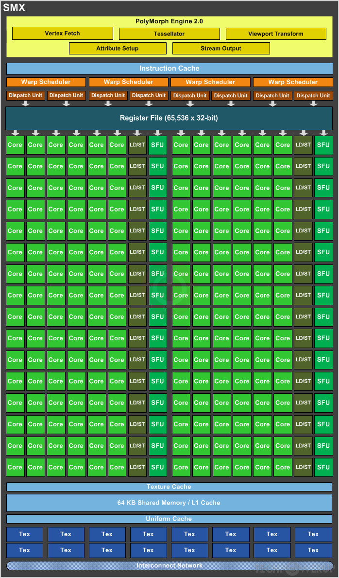
SMX Diagram
NVIDIA's GK20A GPU uses the Kepler 2.0 architecture and is made using a 28 nm production process at TSMC. GK20A supports DirectX 12 (Feature Level 11_0). For GPU compute applications, OpenCL version N/A and CUDA 3.2 can be used. It features 192 shading units, 8 texture mapping units and 4 ROPs.
Further reading:
Tegra K1 Architecture Whitepaper 
Graphics Processor
- Released
- Oct 15th, 2014
- GPU Name
- GK20A
- Codename
- NVEA
- Architecture
- Kepler 2.0
- Foundry
- TSMC
- Process Size
- 28 nm
- Transistors
- unknown
- Die Size
- unknown
Graphics Features
- DirectX
- 12 (11_0)
- OpenGL
- ES 3.1
- OpenCL
- N/A
- Vulkan
- 1.3
- CUDA
- 3.2
- Shader Model
- 6.5 (5.1)
- PureVideo HD
- VP5
- VDPAU
- Feature Set D
Render Config
- Shading Units
- 192
- TMUs
- 8
- ROPs
- 4
- SMX Count
- 1
- GPCs
- 1
- Tex L1 Cache
- 48 KB per SMX
- L1 Cache
- 16 KB per SMX
- L2 Cache
- 128 KB
- Max. TDP
- 8 W
- SFUs
- 32
All Kepler 2.0 GPUs
- NVIDIA GK208
- NVIDIA GK208B
- NVIDIA GK20A
- NVIDIA GK210
NVIDIA GPU Architecture History
- 2025 Blackwell 2.0
- 2024 Blackwell
- 2023 Hopper
- 2022-2024 Ada Lovelace
- 2020-2024 Ampere
- 2018-2022 Turing
- 2017-2020 Volta
- 2016-2021 Pascal
- 2014-2019 Maxwell 2.0
- 2014-2017 Maxwell
- 2013-2015 Kepler 2.0
- 2012-2018 Kepler
- 2010-2016 Fermi 2.0
- 2010-2013 VLIW Vec4
- 2010-2016 Fermi
- 2007-2013 Tesla 2.0
- 2006-2010 Tesla
- 2003-2013 Curie
- 2003-2005 Rankine
- 2001-2003 Kelvin
- 1999-2005 Celsius
- 1998-2000 Fahrenheit
Graphics cards using the NVIDIA GK20A GPU
| Name | Chip | Memory | Shaders | TMUs | ROPs | Base Clock | Boost Clock | Memory Clock |
|---|---|---|---|---|---|---|---|---|
| CD575M-A1 | 2 GB | 192 | 8 | 4 | 756 MHz | 951 MHz | 467 MHz |

GK20A GPU Notes
| L1 Cache is configurable from 16 KB up to 48 KB per SMX |
Jul 18th, 2024 07:33 EDT
change timezone
Latest GPU Drivers
New Forum Posts
- 29"~32" monitor under 300€ (9)
- DTS:X APO4 + DTS Interactive for Most Devices [USB Supported] (310)
- Which brand and model of laptop should I buy? (50)
- How do i get drivers for graphis card on 2000? (10)
- Lexar NQ790, what's the difference from the Lexar NM790? (5)
- Screenshot app for windows 11 that works every time (5)
- What are you playing? (21111)
- Intel Optane 905P 1.5TB $349, $50 off w/ promo (18)
- Is the ThermalRight Frozen Prism 360 AIO good? (109)
- Photobucket new terms of use (7)
Popular Reviews
- AMD Zen 5 Technical Deep Dive
- Noctua NH-D15 G2 Review - Big Performance, Bigger Price
- MCHOSE AX5 Pro Max Review
- Alphacool Core 1 LT CPU Water Block Review
- ID-Cooling FROZN A620 PRO SE Review - Better Value Than Thermalright
- HIFIMAN Susvara Unveiled Planar Magnetic Headphones Review
- Quick Look: Jelly Key Dragons of Eden Ethereal Runes Artisan Keycaps
- AMD Ryzen 7 7800X3D Review - The Best Gaming CPU
- Upcoming Hardware Launches 2024 (Updated May 2024)
- The First Descendant Performance Benchmark Review - 30 GPUs Tested
Controversial News Posts
- Legendary Overclocker KINGPIN Leaves EVGA and Joins PNY to Develop Next-Generation GPUs for Extreme OC (195)
- NVIDIA GeForce RTX 50 Series "Blackwell" TDPs Leaked, All Powered by 16-Pin Connector (165)
- Noctua Announces $150 Flagship NH-D15 G2 CPU Coolers and NF-A14x25r G2 140mm Fans (164)
- Microsoft Closer to Removing Local Accounts from Windows 11, Removes Help Page on How to Switch to One (142)
- AMD is Becoming a Software Company. Here's the Plan (139)
- First Reviews are Live and Snapdragon X Elite Doesn't Quite Deliver on Promised Performance (124)
- AMD to Revise Specs of Ryzen 7 9700X to Increase TDP to 120W, to Beat 7800X3D (112)
- Intel "Arrow Lake-S" to See a Rearrangement of P-cores and E-cores Along the Ringbus (100)