Report an Error


NVIDIA NV37
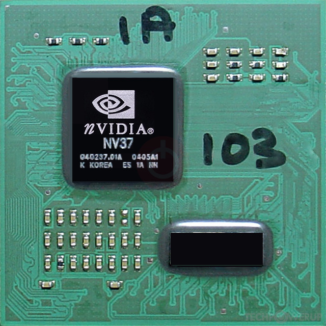
NV37

Die Shot
NVIDIA's NV37 GPU uses the Rankine architecture and is made using a 150 nm production process at TSMC. With a die size of 91 mm² and a transistor count of 45 million it is a very small chip. NV37 supports DirectX 9.0a. Modern GPU compute technologies are not available. It features 4 pixel shaders and 2 vertex shaders, 4 texture mapping units and 4 ROPs. Due to the lack of unified shaders you will not be able to run recent games at all (which require unified shader/DX10+ support).
Graphics Processor
- Released
- Feb 17th, 2004
- GPU Name
- NV37
- Architecture
- Rankine
- Foundry
- TSMC
- Process Size
- 150 nm
- Transistors
- 45 million
- Density
- 494.5K / mm²
- Die Size
- 91 mm²
Graphics Features
- DirectX
- 9.0a
- OpenGL
-
1.5 (full)
2.0 (partial)
- OpenCL
- N/A
- Vulkan
- N/A
- Pixel Shader
- 2.0a
- Vertex Shader
- 2.0a
- WDDM
- 1.0
Render Config
- Pixel Shaders
- 4
- Vertex Shaders
- 2
- TMUs
- 4
- ROPs
- 4
- Max. TDP
- 21 W
All Rankine GPUs
NVIDIA GPU Architecture History
- 2025 Blackwell 2.0
- 2024-2025 Blackwell
- 2023 Hopper
- 2022-2024 Ada Lovelace
- 2020-2024 Ampere
- 2018-2022 Turing
- 2017-2020 Volta
- 2016-2021 Pascal
- 2014-2019 Maxwell 2.0
- 2014-2017 Maxwell
- 2013-2015 Kepler 2.0
- 2012-2018 Kepler
- 2010-2016 Fermi 2.0
- 2010-2013 VLIW Vec4
- 2010-2016 Fermi
- 2007-2013 Tesla 2.0
- 2006-2010 Tesla
- 2003-2013 Curie
- 2003-2005 Rankine
- 2001-2003 Kelvin
- 1999-2005 Celsius
- 1998-2000 Fahrenheit
Graphics cards using the NVIDIA NV37 GPU
| Name | Chip | Memory | Shaders | TMUs | ROPs | GPU Clock | Memory Clock |
|---|---|---|---|---|---|---|---|
| 128 MB | 4 / 2 | 4 | 4 | 250 MHz | 200 MHz | ||
| NV37 GL | 64 MB | 4 / 2 | 4 | 4 | 250 MHz | 200 MHz | |
| NV37 GL | 64 MB | 4 / 2 | 4 | 4 | 275 MHz | 250 MHz |


NV37 GPU Notes
| NV37 = NV34 + HSI Latest Drivers: Windows NT 4: ForceWare Release 77.56 ForceWare Release 77.72 Desktop Windows 95 / 98 / ME: ForceWare Release 81.98 Windows 2000: GeForce Release 93.71 / 93.81 Beta Quadro Release 169.96 Windows XP / Server 2003 x64: GeForce Release 175.19 Quadro Release 169.96 Windows Vista: ForceWare Release 96.85 |
Oct 18th, 2024 03:41 EDT
change timezone
Latest GPU Drivers
New Forum Posts
- Which 20 TB drive to get? (122)
- Help needed: can't get Realtek ALC1200 working on MSI B550M motherboard under Windows 7 (33)
- installing linux mint with some cinnamon on ssd (4)
- PSA: Do not buy from gigantti. (18)
- :O Limits of air cooling [Intel] (37)
- Ghetto Mods (4458)
- Post your Speedtest.net Speeds! (2308)
- DTS DCH Driver for Realtek HDA [DTS:X APO4 + DTS Interactive] (2002)
- Looking for a a new low power trio for my home studio (43)
- [Detailed + Need Help] Interesting Undervolting Lock(?) Situation on HP Victus 16 r1xxx (5)
Popular Reviews
- ASRock DeskMini X600 Barebones Mini-PC (Ryzen 8600G) Review
- Corsair 9000D RGB Airflow Review
- 64 Audio Solo Planar Magnetic IEMs Review
- Lian Li O11 Vision Compact Review
- Silent Hill 2 Remake Handheld Performance Review
- Logitech G Pro X Superlight 2 Review - Updated with 8000 Hz Tested
- Silent Hill 2 Remake Performance Benchmark Review - 35 GPUs Tested
- HAVN HS 420 VGPU Review
- Intel Core Ultra Arrow Lake Preview
- Montech King 65 Pro Review
Controversial News Posts
- NVIDIA GeForce RTX 5090 and RTX 5080 Specifications Surface, Showing Larger SKU Segmentation (183)
- AMD Ryzen 9 9950X3D and 9900X3D to Feature 3D V-cache on Both CCD Chiplets (127)
- Quick Denuvo DRM Cracks Cost Game Publishers 20% in Revenue, According to Study (125)
- MSI OCLab Reveals Ryzen 9000X3D 11-13% Faster Than 7000X3D, AMD Set to Dominate "Arrow Lake" in Gaming (123)
- AMD Rushing in Ryzen 7 9800X3D, Expect Product Launch Late-October (117)
- Single-Player Games Lose to PVP in Younger Audiences Despite Recent Hits (116)
- NVIDIA Tunes GeForce RTX 5080 GDDR7 Memory to 32 Gbps, RTX 5070 Launches at CES (112)
- Intel's Core Ultra 9 285K Performance Claims Leaked, Doesn't Beat i9-14900K at Gaming (111)