Report an Error


NVIDIA NV30

NV30

NV30GL
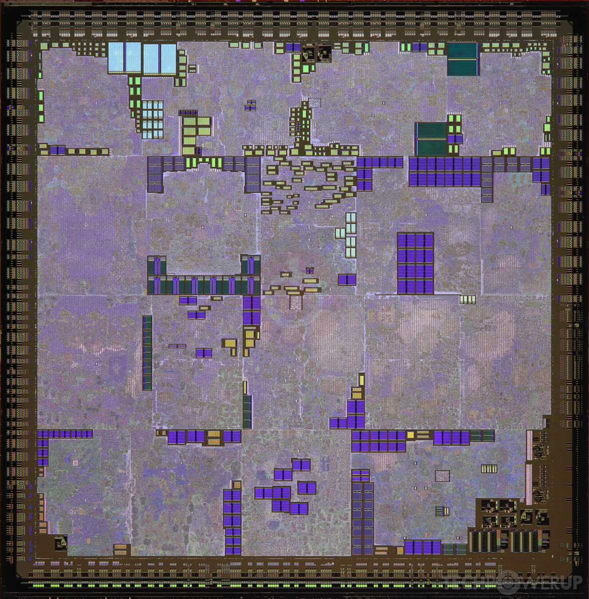
Die Shot

Block Diagram

Block Diagram 2
NVIDIA's NV30 GPU uses the Rankine architecture and is made using a 130 nm production process at TSMC. With a die size of 199 mm² and a transistor count of 125 million it is a small chip. NV30 supports DirectX 9.0a. Modern GPU compute technologies are not available. It features 4 pixel shaders and 3 vertex shaders, 8 texture mapping units and 4 ROPs. Due to the lack of unified shaders you will not be able to run recent games at all (which require unified shader/DX10+ support).
Graphics Processor
- Released
- Jan 21st, 2003
- GPU Name
- NV30
- Architecture
- Rankine
- Foundry
- TSMC
- Process Size
- 130 nm
- Transistors
- 125 million
- Density
- 628.1K / mm²
- Die Size
- 199 mm²
Graphics Features
- DirectX
- 9.0a
- OpenGL
-
1.5 (full)
2.0 (partial)
- OpenCL
- N/A
- Vulkan
- N/A
- Pixel Shader
- 2.0a
- Vertex Shader
- 2.0a
- WDDM
- 1.0
Render Config
- Pixel Shaders
- 4
- Vertex Shaders
- 3
- TMUs
- 8
- ROPs
- 4
- Max. TDP
- 44 W
All Rankine GPUs
NVIDIA GPU Architecture History
- 2025 Blackwell 2.0
- 2024 Blackwell
- 2023 Hopper
- 2022-2024 Ada Lovelace
- 2020-2024 Ampere
- 2018-2022 Turing
- 2017-2020 Volta
- 2016-2021 Pascal
- 2014-2019 Maxwell 2.0
- 2014-2017 Maxwell
- 2013-2015 Kepler 2.0
- 2012-2018 Kepler
- 2010-2016 Fermi 2.0
- 2010-2013 VLIW Vec4
- 2010-2016 Fermi
- 2007-2013 Tesla 2.0
- 2006-2010 Tesla
- 2003-2013 Curie
- 2003-2005 Rankine
- 2001-2003 Kelvin
- 1999-2005 Celsius
- 1998-2000 Fahrenheit
Graphics cards using the NVIDIA NV30 GPU
| Name | Chip | Memory | Shaders | TMUs | ROPs | GPU Clock | Memory Clock |
|---|---|---|---|---|---|---|---|
| 128 MB | 4 / 3 | 8 | 4 | 500 MHz | 500 MHz | ||
| 128 MB | 4 / 3 | 8 | 4 | 400 MHz | 400 MHz | ||
| NV30GL | 128 MB | 4 / 3 | 8 | 4 | 300 MHz | 300 MHz | |
| NV30GL | 128 MB | 4 / 3 | 8 | 4 | 400 MHz | 400 MHz |


NV30 GPU Notes
| Latest Drivers: Windows NT 4: ForceWare Release 77.56 ForceWare Release 77.72 Desktop Windows 95 / 98 / ME: ForceWare Release 81.98 Windows 2000: GeForce Release 93.71 / 93.81 Beta Quadro Release 169.96 Windows XP / Server 2003 x64: GeForce Release 175.19 Quadro Release 169.96 Windows Vista: ForceWare Release 96.85 |
Nov 18th, 2024 08:18 EST
change timezone
Latest GPU Drivers
New Forum Posts
- Technical Issues - TPU Main Site & Forum (2024) (367)
- Upgrade from 13700k to 9800X3D (RAM issues?) (35)
- getting BSOD on certain games (10)
- whats going on with core 2 quad and windows? (44)
- NVIDIA App (34)
- GPU Test System 2025 Games Selection (31)
- What Was Your First... (Gaming Related Things) (10)
- Anyone using a MSI MEG Z890 Ace? (0)
- Fixing USB flash drive? (3)
- Anime Nation (12894)
Popular Reviews
- AMD Ryzen 7 9800X3D Review - The Best Gaming Processor
- NVIDIA App v1.0 Review
- Redragon K1NG 8K Review
- Quick Look: MOONDROP Quark2 Type-C In-Ear Monitors
- Valkyrie VK02 Lite Review
- Epomaker TH40 Wireless Mechanical Keyboard Review
- Quick Look: G.SKILL WigiDash PC Command Panel
- Beelink GTi12 Ultra Mini-PC + EX Dock (Intel Core i9-12900H) Review
- Upcoming Hardware Launches 2024 (Updated Nov 2024)
- ASUS GeForce RTX 4060 Dual OC Review - The Best RTX 4060
Controversial News Posts
- AMD Falling Behind: Radeon dGPUs Absent from Steam's Top 20 (222)
- AMD Ryzen 7 9800X3D Stocks Vaporized in Retail, Being Scalped (151)
- AMD Introduces Next-Generation AMD Ryzen 7 9800X3D Processor, $479, Nov 7 (124)
- Apple and Samsung in the Fray to Acquire Intel: Rumor (123)
- AMD Ryzen 7 9800X3D Comes with 120W TDP, 5.20 GHz Boost, All Specs Leaked (120)
- Microsoft Offers $30 Windows 10 Security Extension for Home Users (118)
- AMD Ryzen 7 9800X3D Has the CCD on Top of the 3D V-cache Die, Not Under it (110)
- TechPowerUp is Hiring a Power Supply (PSU) Reviewer (106)