Report an Error


NVIDIA Quadro K3100M
- Graphics Processor
- GK104
- Cores
- 768
- TMUs
- 64
- ROPs
- 32
- Memory Size
- 4 GB
- Memory Type
- GDDR5
- Bus Width
- 256 bit

GPU
Recommended Gaming Resolutions:
- 1366x768
- 1600x900
- 1920x1080
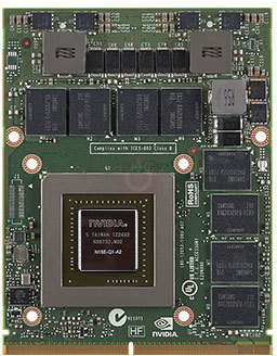
The Quadro K3100M was a professional mobile graphics chip by NVIDIA, launched on July 23rd, 2013. Built on the 28 nm process, and based on the GK104 graphics processor, in its N15E-Q1-A2 variant, the chip supports DirectX 12. The GK104 graphics processor is an average sized chip with a die area of 294 mm² and 3,540 million transistors. Unlike the fully unlocked GeForce GTX 680, which uses the same GPU but has all 1536 shaders enabled, NVIDIA has disabled some shading units on the Quadro K3100M to reach the product's target shader count. It features 768 shading units, 64 texture mapping units, and 32 ROPs. NVIDIA has paired 4 GB GDDR5 memory with the Quadro K3100M, which are connected using a 256-bit memory interface. The GPU is operating at a frequency of 706 MHz, which can be boosted up to 706 MHz, memory is running at 800 MHz (3.2 Gbps effective).
Being a mxm module card, the NVIDIA Quadro K3100M does not require any additional power connector, its power draw is rated at 75 W maximum. This device has no display connectivity, as it is not designed to have monitors connected to it. Rather it is intended for use in laptop/notebooks and will use the output of the host mobile device.
Being a mxm module card, the NVIDIA Quadro K3100M does not require any additional power connector, its power draw is rated at 75 W maximum. This device has no display connectivity, as it is not designed to have monitors connected to it. Rather it is intended for use in laptop/notebooks and will use the output of the host mobile device.
Graphics Processor
Mobile Graphics
- Release Date
- Jul 23rd, 2013
- Generation
-
Quadro Kepler-M
(Kx100M)
- Predecessor
- Quadro Fermi-M
- Successor
- Quadro Maxwell-M
- Production
- End-of-life
- Bus Interface
- MXM-B (3.0)
- Reviews
- 26 in our database
Relative Performance
Based on TPU review data: "Performance Summary" at 1920x1080, 4K for 2080 Ti and faster.
Performance estimated based on architecture, shader count and clocks.
Clock Speeds
- Base Clock
- 706 MHz
- Boost Clock
- 706 MHz
- Memory Clock
-
800 MHz
3.2 Gbps effective
Memory
- Memory Size
- 4 GB
- Memory Type
- GDDR5
- Memory Bus
- 256 bit
- Bandwidth
- 102.4 GB/s
Render Config
- Shading Units
- 768
- TMUs
- 64
- ROPs
- 32
- SMX Count
- 4
- L1 Cache
- 16 KB (per SMX)
- L2 Cache
- 512 KB
Theoretical Performance
- Pixel Rate
- 11.30 GPixel/s
- Texture Rate
- 45.18 GTexel/s
- FP32 (float)
- 1,084 GFLOPS
- FP64 (double)
- 45.18 GFLOPS (1:24)
Board Design
- Slot Width
- MXM Module
- TDP
- 75 W
- Outputs
- Portable Device Dependent
- Power Connectors
- None
- Board Number
- P2053 SKU 501
Graphics Features
- DirectX
- 12 (11_0)
- OpenGL
- 4.6
- OpenCL
- 3.0
- Vulkan
- 1.2.175
- CUDA
- 3.0
- Shader Model
- 6.5 (5.1)
GK104 GPU Notes
| NVENC: 1st Gen NVDEC: 1st Gen PureVideo HD: VP5 VDPAU: Feature Set D L1 Cache is configurable from 16 KB up to 48 KB per SMX Latest Drivers: Windows XP / Server 2003 x64: Quadro Release R319 U2 (321.01) Windows Vista: GeForce Release 365.19 Quadro Release R346 U7 (348.40) / R352 BETA (352.86) Windows 7 / 8 / 8.1 / 10 / 11 (x32 / x64): GeForce Release 391.35 / 475.06 Quadro Release R390 U9 (392.37) / R470 U16 (474.82) Data Center Release 427.11 Tesla Release 441.22 Windows 10 / 11 x64: GeForce Release 475.06 Quadro Release R470 U16 (474.82) Data Center Release 474.82 |
Jul 19th, 2024 04:16 EDT
change timezone
Latest GPU Drivers
New Forum Posts
- TPU's Nostalgic Hardware Club (18760)
- Graphics card only runs with X1 instead X16 (28)
- What's your latest tech purchase? (21082)
- What are you playing? (21117)
- The TPU UK Clubhouse (25013)
- Upgrade from Acer XB271HUC IPS? (9)
- Intel Optane 905P 1.5TB $349, $50 off w/ promo (26)
- Free Games Thread (3944)
- Any other game like resident evil 1? (62)
- Windows 11 General Discussion (5250)
Popular Reviews
- AMD Zen 5 Technical Deep Dive
- Noctua NH-D15 G2 Review - Big Performance, Bigger Price
- MCHOSE AX5 Pro Max Review
- Audeze MM-500 Open-Back Planar Magnetic Headphones Review
- Alphacool Core 1 LT CPU Water Block Review
- ID-Cooling FROZN A620 PRO SE Review - Better Value Than Thermalright
- Upcoming Hardware Launches 2024 (Updated May 2024)
- HIFIMAN Susvara Unveiled Planar Magnetic Headphones Review
- AMD Ryzen 7 7800X3D Review - The Best Gaming CPU
- The First Descendant Performance Benchmark Review - 30 GPUs Tested
Controversial News Posts
- Legendary Overclocker KINGPIN Leaves EVGA and Joins PNY to Develop Next-Generation GPUs for Extreme OC (195)
- NVIDIA GeForce RTX 50 Series "Blackwell" TDPs Leaked, All Powered by 16-Pin Connector (165)
- Noctua Announces $150 Flagship NH-D15 G2 CPU Coolers and NF-A14x25r G2 140mm Fans (164)
- Microsoft Closer to Removing Local Accounts from Windows 11, Removes Help Page on How to Switch to One (142)
- AMD is Becoming a Software Company. Here's the Plan (139)
- AMD to Revise Specs of Ryzen 7 9700X to Increase TDP to 120W, to Beat 7800X3D (112)
- Intel Planning P-core Only "Bartlett" LGA1700 Processor for 2025 (105)
- Intel "Arrow Lake-S" to See a Rearrangement of P-cores and E-cores Along the Ringbus (100)