News Posts matching #2025

Return to Keyword Browsing

Intel Sets 100 Million CPU Supply Goal for AI PCs by 2025

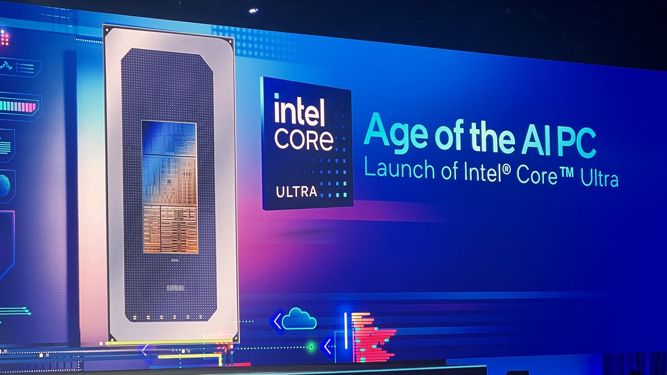
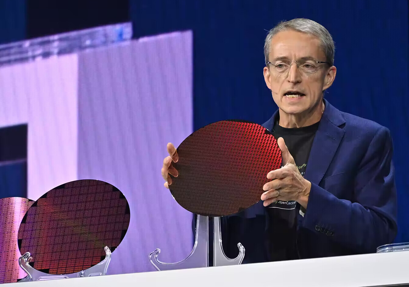
Intel has been hyping up their artificial intelligence-augmented processor products since late last year—their "AI Everywhere" marketing push started with the official launch of Intel Core Ultra mobile CPUs, AKA the much-delayed Meteor Lake processor family. CEO, Pat Gelsinger stated (mid-December 2023): "AI innovation is poised to raise the digital economy's impact up to as much as one-third of global gross domestic product...Intel is developing the technologies and solutions that empower customers to seamlessly integrate and effectively run AI in all their applications—in the cloud and, increasingly, locally at the PC and edge, where data is generated and used." Team Blue's presence at this week's MWC Barcelona 2024 event introduced "AI Everywhere Across Network, Edge, Enterprise."

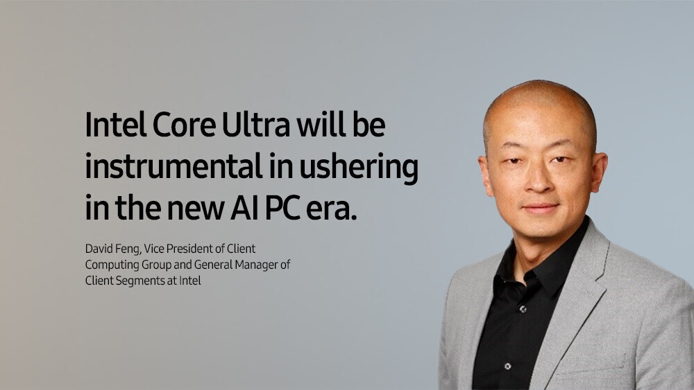
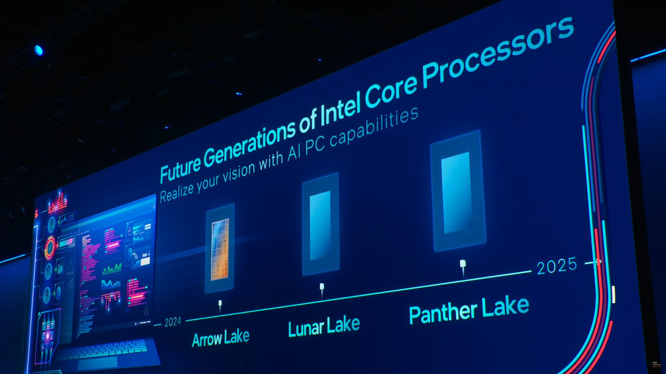
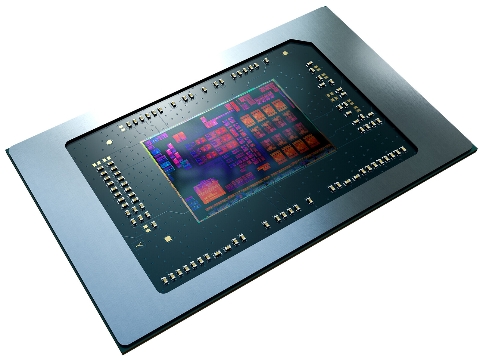
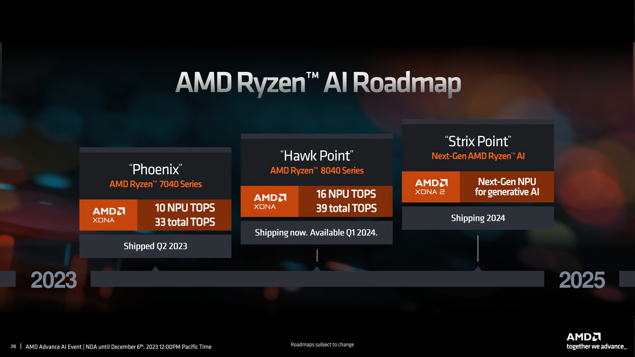
Nikkei Asia sat down with Intel's David Feng—Vice President of Client Computing Group and General Manager of Client Segments. The impressively job-titled executive discussed the "future of AI PCs," and set some lofty sales goals for his firm. According to the Nikkei report, Intel leadership expects to "deliver 40 million AI PCs" this year and a further 60 million units next year—representing "more than 20% of the projected total global PC market in 2025." Feng and his colleagues predict that mainstream customers will prefer to use local "on-device" AI solutions (equipped with NPUs), rather than rely on remote cloud services. Significant Edge AI improvements are expected to arrive with next generation Lunar Lake and Arrow Lake processor families, the latter will be bringing Team Blue NPU technologies to desktop platforms—AMD's Ryzen 8000G series of AM5 APUs launched with XDNA engines last month.

Samsung Bags 2 nm Wafer Order from Japanese AI Chip Startup

Samsung Electronics foundry has reportedly bagged a mass production order for its cutting edge 2 nm EUV foundry node from Japanese AI chip startup PFN (Preferred Networks). This is reportedly the first major third party order for the 2 nm node. Founded in 2014, PFN specializes in AI and IoT chips, and spun off from Preferred Infrastructure. Samsung's 2 nm node, called the SF2, is on track for delivery of mass produced chips in 2025, which means much of 2024 will be spent on testing, validation, and risk production, with the node expected to go live toward the end of the year. Samsung SF2 is being designed to offer 25% higher power efficiency (at iso-clocks), and 12% increase in performance, over SF3 (3 nm EUV FinFET). In the semiconductor fabrication market, Samsung SF2 competes against TSMC N2 and Intel 20A.

Nintendo Switch 2 Launch Window Reportedly Shifts to Early 2025

Murmurings of a delayed Nintendo "Switch 2" release schedule appeared online earlier this week—Brazilian games journalist, Pedro Henrique Lutti Lippe, made claims during an "OX do Controle" videocast—based on insider information. Additionally, he broke the bad news on social media: "Nobody wants to hear this, but this one is pretty intense. After consulting five sources from three different continents, all echoing basically the same thing, we can reveal (that) the launch of the Switch's successor should only happen in 2025." Several global news outlets have performed their own investigations, following up on OX do Controle's declaration.

Eurogamer reached out to its network of "trusty" insiders—their Friday evening update stated that: "(we) can now corroborate the earlier reports/whispers that the Switch 2, once destined for release later in 2024, is now set for Q1 2025...The console's launch moving into early next year—but still within the coming financial year—is designed to ensure Switch 2's launch line-up features as many titles as possible, Eurogamer understands." Video Games Chronicle's Andy Robinson has similarly checked in with his pool of industry spies: "VGC has heard from multiple sources who said Nintendo has told publishers its next console will now launch in Q1 2025. According to the sources, third-party game companies were recently briefed on an internal delay in Nintendo's next-gen launch timing, from late 2024 to early the following year. One publishing source suggested the delay was so that Nintendo could prepare stronger first-party software for the console. It's possible the next-gen Nintendo console will now follow a similar timeline to the Switch, which was released in March but announced the previous year."

ASML High-NA EUV Twinscan EXE Machines Cost $380 Million, 10-20 Units Already Booked

ASML has revealed that its cutting-edge High-NA extreme ultraviolet (EUV) chipmaking tools, called High-NA Twinscan EXE, will cost around $380 million each—over twice as much as its existing Low-NA EUV lithography systems that cost about $183 million. The company has taken 10-20 initial orders from the likes of Intel and SK Hynix and plans to manufacture 20 High-NA systems annually by 2028 to meet demand. The High-NA EUV technology represents a major breakthrough, enabling an improved 8 nm imprint resolution compared to 13 nm with current Low-NA EUV tools. This allows chipmakers to produce transistors that are nearly 1.7 times smaller, translating to a threefold increase in transistor density on chips. Attaining this level of precision is critical for manufacturing sub-3 nm chips, an industry goal for 2025-2026. It also eliminates the need for complex double patterning techniques required presently.

However, superior performance comes at a cost - literally and figuratively. The hefty $380 million price tag for each High-NA system introduces financial challenges for chipmakers. Additionally, the larger High-NA tools require completely reconfiguring chip fabrication facilities. Their halved imaging field also necessitates rethinking chip designs. As a result, adoption timelines differ across companies - Intel intends to deploy High-NA EUV at an advanced 1.8 nm (18A) node, while TSMC is taking a more conservative approach, potentially implementing it only in 2030 and not rushing the use of these lithography machines, as the company's nodes are already developing well and on time. Interestingly, the installation process of ASML's High-NA Twinscan EXE 150,000-kilogram system required 250 crates, 250 engineers, and six months to complete. So, production is as equally complex as the installation and operation of this delicate machinery.

Kojima Shows Off "Death Stranding 2: On The Beach" During PlayStation Event

Sony Interactive Entertainment's State of Play confirming the title of the game, DEATH STRANDING 2: ON THE BEACH, arriving exclusively on PlayStation 5 in 2025. In Death Stranding 2: On The Beach, embark on an inspiring mission of human connection beyond the UCA. Sam—with companions by his side—sets out on a new journey to save humanity from extinction. Join them as they traverse a world beset by otherworldly enemies, obstacles and a haunting question: should we have connected? Step by step, legendary game creator Hideo Kojima changes the world once again.

Death Stranding 2: On The Beach sees Norman Reedus, Léa Seydoux, and Troy Baker return to Hideo Kojima's genre defying universe. They will be joined by Elle Fanning, Shioli Kutsuna, and Academy Award-winning film director George Miller. Hideo Kojima is joined by longtime collaborator Yoji Shinkawa who will direct character and mechanical design, with Ludvig Forssell and Kyle Cooper reprising their roles as musical director and title designer, respectively. In conjunction with the release of the new Death Stranding 2: On The Beach trailer, be sure to visit the PS5 Game Hub to add the game to your wishlist and stay tuned for more information!

SK Hynix Targets HBM3E Launch This Year, HBM4 by 2026

SK Hynix has unveiled ambitious High Bandwidth Memory (HBM) roadmaps at SEMICON Korea 2024. Vice President Kim Chun-hwan announced plans to mass produce the cutting-edge HBM3E within the first half of 2024, touting 8-layer stack samples already supplied to clients. This iteration makes major strides towards fulfilling surging data bandwidth demands, offering 1.2 TB/s per stack and 7.2 TB/s in a 6-stack configuration. VP Kim Chun-hwan cites the rapid emergence of generative AI, forecasted for 35% CAGR, as a key driver. He warns that "fierce survival competition" lies ahead across the semiconductor industry amidst rising customer expectations. With limits approaching on conventional process node shrinks, attention is shifting to next-generation memory architectures and materials to unleash performance.

SK Hynix has already initiated HBM4 development for sampling in 2025 and mass production the following year. According to Micron, HBM4 will leverage a wider 2048-bit interface compared to previous HBM generations to increase per-stack theoretical peak memory bandwidth to over 1.5 TB/s. To achieve these high bandwidths while maintaining reasonable power consumption, HBM4 is targeting a data transfer rate of around 6 GT/s. The wider interface and 6 GT/s speeds allow HBM4 to push bandwidth boundaries significantly compared to prior HBM versions, fueling the need for high-performance computing and AI workloads. But power efficiency is carefully balanced by avoiding impractically high transfer rates. Additionally, Samsung is aligned on a similar 2025/2026 timeline. Beyond pushing bandwidth boundaries, custom HBM solutions will become increasingly crucial. Samsung executive Jaejune Kim reveals that over half its HBM volume already comprises specialized products. Further tailoring HBM4 to individual client needs through logic integration presents an opportunity to cement leadership. As AI workloads evolve at breakneck speeds, memory innovation must keep pace. With HBM3E prepping for launch and HBM4 in the plan, SK Hynix and Samsung are gearing up for the challenges ahead.

Intel "Panther Lake" Targets Substantial AI Performance Leap in 2025

Pat Gelsinger, CEO of Intel Corporation, has outlined future performance expectations for the company's Core range of processors. In a recent fourth quarter 2023 earnings call he declared: "The Core Ultra platform delivers leadership AI performance today with our next-generation platforms launching later this year, Lunar Lake and Arrow Lake tripling our AI performance. In 2025 with Panther Lake, we will grow AI performance up to an additional 2x." Team Blue's Intel Core Ultra "Meteor Lake" mobile processors arrived right at the tail end of last year, as a somewhat delayed answer to AMD's Ryzen 7040 "Phoenix" APU series—both leveraging their own AI-crunching NPU technologies. Gelsinger believes that the launch of Lunar Lake and Arrow Lake Core product lines will bring significant (3x) AI processing improvements over Meteor Lake. He seemed to confident in a delay-free release schedule for the new year and beyond: "We are first in the industry to have incorporated both gate-all-around and backside power delivery in a single process node, the latter unexpected two years ahead of our competition. Arrow Lake, our lead Intel 20A vehicle will launch this year."

He proceeded to gush about their next node advancement: "Intel 18A is expected to achieve manufacturing readiness in second half 2024, completing our five nodes in four year journey and bringing us back to process leadership. I am pleased to say that Clearwater Forest, our first Intel 18A part for servers has already gone into fab and Panther Lake for clients will be heading into Fab shortly." Industry experts posit that Core "Panther Lake" parts could borrow elements from the next generation Xeon "Clearwater Forest" efficiency-focused family—possibly the latter's "Darkmont" E-cores, to accompany "Cougar Cove" P-cores. The Intel CEO is quite excited about the manufacturing outlay for 2025: "I'll just say, hey, we look at this every single day and we're scrutinizing carefully our progress on 18A. And obviously the great news that we just described those Clearwater Forest taping out, that gives us a lot of confidence that 18A is healthy. That's a major product for us. Panther Lake following that shortly."

Tipster Claims AMD "Kraken Point" APU Configured with Zen 5 & Zen 5c Cores

Everest (@Olrak29_) has kept track of many AMD processor families over the past couple of years—his latest insight provides an early look at the alleged internal makeup of Team Red's "Kraken Point" APU series. The rumor mill has designated these next-gen mobile processors as 2025 follow-ups to the recently launched Ryzen 8040 "Hawk Point" family of mainstream laptop APUs. The tipster's initial social media post only mentioned the presence of both Zen 5 and Zen 5c cores within Kraken Point processors, but he later clarified that a total of eight cores would include four large units and four smaller types. TPU's past coverage of Kraken Point pointed to rumors of an 8-core, 16-thread configuration, but leaked slides (from late 2023) did not mention the integration of efficiency-tuned Zen 5c "Prometheus" cores, along with presumed Zen 5 "Nirvana" cores.

Everest's continuous flow of insider information reveals that "Kraken Point" shares many "Hawk Point" traits—four workgroup processors (WGP) could be present on final retail products, granting eight compute units (8 CUs in total). He responded to a query regarding AMD's choice of integrated graphics technology—the succinct answer being RDNA 3.5. Past leaks allege that XDNA 2 will drive the NPU side of things—offering a performance range of around 45 to 50 TOPS. The Kraken Point APU is believed to be sticking with a safe monolithic die design, manufactured on a non-specific 4 nm process. Team Red is rumored to be in TSMC's order books for all sorts of next generation silicon.

Apple Reportedly in the VVIP Lane for TSMC's 2 Nanometer GAA

A DigiTimes Asia report posits that TSMC is preparing another VVIP foundry lane for Apple Inc.—insiders claim that the Taiwanese foundry giant is in the process of expanding production capacity into next generation 2 nm nanometer fields. This expensive and time consuming endeavor is only made possible with the reassurance of big customers being added to the foundry's order books. TSMC's 2 nm-class N2, N2P, and N2X process technologies are due in 2025 and beyond (according to recent presentation slides)—these advanced packages are set to drop with all sorts of innovations: nanosheet gate-all-around (GAA) transistors, backside power delivery, and super-high-performance metal-insulator-metal (SHPMIM). According to a DigiTimes source "Apple is widely believed to be the initial client to utilize the (next-gen) process."

Apple and NVIDIA were reported to be ahead of many important clients in the queue for TSMC's 3 nm process nodes, so it is not surprising to see old patterns repeat (according to industry rumors) again. Apple is expected to update its next generation iPhones, iPad, and Mac laptop product lines with more advanced Bionic and M-series chipsets in 2025. Last year's roster included a rollout of 3 nm TSMC silicon across Apple A17 Pro and M3 ARM-based processors.

HBM Industry Revenue Could Double by 2025 - Growth Driven by Next-gen AI GPUs Cited

Samsung, SK hynix, and Micron are considered to be the top manufacturing sources of High Bandwidth Memory (HBM)—the HBM3 and HBM3E standards are becoming increasingly in demand, due to a widespread deployment of GPUs and accelerators by generative AI companies. Taiwan's Commercial Times proposes that there is an ongoing shortage of HBM components—but this presents a growth opportunity for smaller manufacturers in the region. Naturally, the big name producers are expected to dive in head first with the development of next generation models. The aforementioned financial news article cites research conducted by the Gartner group—they predict that the HBM market will hit an all-time high of $4.976 billion (USD) by 2025.

This estimate is almost double that of projected revenues (just over $2 billion) generated by the HBM market in 2023—the explosive growth of generative AI applications has "boosted" demand for the most performant memory standards. The Commercial Times report states that SK Hynix is the current HBM3E leader, with Micron and Samsung trailing behind—industry experts believe that stragglers will need to "expand HBM production capacity" in order to stay competitive. SK Hynix has shacked up with NVIDIA—the GH200 Grace Hopper platform was unveiled last summer; outfitted with the South Korean firm's HBM3e parts. In a similar timeframe, Samsung was named as AMD's preferred supplier of HBM3 packages—as featured within the recently launched Instinct MI300X accelerator. NVIDIA's HBM3E deal with SK Hynix is believed to extend to the internal makeup of Blackwell GB100 data-center GPUs. The HBM4 memory standard is expected to be the next major battleground for the industry's hardest hitters.

AMD "Strix Point & Strix Halo" Zen 5 APUs Spotted in ROCm GitHub

References to GFX1150 & GFX1151 targets have been spotted again—this time in a ROCm Github repository—by renowned hardware sleuth; Kepler_L2. These references were first spotted last summer, in an AMDGPU LLVM backend/compiler (reported by Phoronix)—industry experts immediately linked these target codes to next generation "Strix" APU families. The latest leak provides confirmation that the GFX1150 ID is tied to "Strix Point 1," while GFX1151 is an internal IP for "Strix Point Halo," or simply "Strix Halo." The freshly published ROCm Github's commit is titled: "Strix Halo Support and Strix support in staging," which corroborates previous rumors regarding Team Red's engineers being deep into development of Zen 5 (and RDNA 3.5)-based accelerated processing units.

AMD has published several processor product roadmaps with references to "Strix Point" next-gen APUs, with a targeted 2024 launch window. Their December 2023 "Advancing AI Event" confirmed that the "Strix Point" mobile family will sport "XDNA 2" NPUs—previous generation "Phoenix" and recently released "Hawk Point" processors are on the first iteration of XDNA (a spatial dataflow NPU architecture). It is speculated that a typical "Strix Point" laptop processor will pack 12 Zen 5 CPU cores and 16 RDNA 3.5 GPU cores. Team Red has kept quiet about "Strix Halo" (also known as "Sarlak") when conducting public-facing presentations—a loose 2025 launch window is being touted by the rumor mill. The most advanced examples could feature up to 16 Zen 5 CPU cores and 40 RDNA 3.5 GPU cores.

Synopsys to Acquire Ansys, Creating a Leader in Silicon to Systems Design Solutions

Synopsys (NASDAQ: SNPS) and Ansys (NASDAQ: ANSS) today announced that they have entered into a definitive agreement under which Synopsys will acquire Ansys. Under the terms of the agreement, Ansys shareholders will receive $197.00 in cash and 0.3450 shares of Synopsys common stock for each Ansys share, representing an enterprise value of approximately $35 billion based on the closing price of Synopsys common stock on December 21, 2023. Bringing together Synopsys' pioneering semiconductor electronic design automation (EDA) with Ansys' broad simulation and analysis portfolio will create a leader in silicon to systems design solutions.

"The megatrends of AI, silicon proliferation and software-defined systems are requiring more compute performance and efficiency in the face of growing, systemic complexity. Bringing together Synopsys' industry-leading EDA solutions with Ansys' world-class simulation and analysis capabilities will enable us to deliver a holistic, powerful and seamlessly integrated silicon to systems approach to innovation to help maximize the capabilities of technology R&D teams across a broad range of industries," said Sassine Ghazi, President and CEO of Synopsys. "This is the logical next step for our successful, seven-year partnership with Ansys and I look forward to working closely with Ajei and the talented Ansys team to realize the benefits of this combination for our customers, shareholders and employees."

Retroware Presents "The Transylvania Adventure of Simon Quest"

From Programancer, the developer of Prison City and Dumpy & Bumpy, comes a brand new title: The Transylvania Adventure of Simon Quest! You're supposed to be the hero, but your spotlight was taken away! Rival Stan Helsing defeated Dracula first, now Simon Quest must embark on a journey of retribution to raise the Count from the dead piece-by-piece, slay him, and obtain the glory he deserves! Go on a perilous journey through the world of Transylvania.

Explore dark mansions, discover minigames, and collect different parts of Dracula to raise him from the dead…then kill him! The Transylvania Adventure of Simon Quest (TASQ) is a parody/homage platformer set in a dark 8-bit world. Reclaim your glory by resurrecting Dracula piece by piece and slaying the dark count yourself! Coming to Steam, Nintendo Switch, PlayStation, Xbox, and Epic in 2025. Stay tuned for more platform announcements. Retroware is excited to announce this new project in development with Programancer! AND, if you're itching to get your hands on playing a preview of The Transylvania Adventure of Simon Quest (TASQ), YOU CAN at MAGFest 2024 at the National Harbor from January 18 to 21!

No GTA 6 for PC Gamers at Launch, Rockstar Confirms

Rockstar Games has officially released a Grand Theft Auto 6 (or VI) trailer that brings together millions of GTA series fans. However, the game will remain exclusive for gaming consoles at launch. On the landing page for GTA 6, there is a note that says, "Grand Theft Auto VI heads to the state of Leonida, home to the neon-soaked streets of Vice City and beyond in the biggest, most immersive evolution of the Grand Theft Auto series yet. Coming 2025 to PlayStation 5 and Xbox Series X|S." While the first trailer showed this, we now have written confirmation that GTA 6 is a console exclusive at launch, whenever it happens in 2025.

If long-time GTA gamers remember, the situation was very much the same with the launch of the fifth installment in the GTA series, GTA V, which got a PC port almost two years after the initial release. The GTA V was released in September 2013 for the PlayStation 3 and Xbox 360 consoles and got an upgrade to a new console cycle in November 2014 for the PlayStation 4 and Xbox One. Only in April 2015 was the game released for Windows-based PCs, as Rockstar took its time to polish the port and make it work with PC gamers' various hardware choices. While we hope to avoid seeing such a big cadence from console to PC port, it will surely take Rockstar some extra time to make a PC version run smoothly.

Apple to Become the First and Largest Customer of Amkor's Arizona Chip Packaging Plant

Apple has announced a partnership deal with Amkor, one of the leading chip packaging and testing manufacturers, which will build a two billion US Dollar silicon packaging facility in Peoria, Arizona. Being the only US-based OSAT (outsourced semiconductor assembly and test) provider, Amkor has decided to invest its funds and apply for the CHIPS Act, hoping to get a part of the funding from the US government's grant budget. The state-of-the-art facility in Arizona will feature over 500,000 square feet (46,452 square meters) of cleanroom space for packaging and testing chips. Using Amkor's latest technologies, the plant will support advanced computing, automotive, and communications chip packaging. It is tailored to meet the capacity needs of major customer Apple starting in 2025-2026. Apple will be the largest customer, with the Amkor facility packaging Apple-designed chips produced at the nearby TSMC wafer fabrication plant.

Building a chip packaging facility in the US with advanced packaging types means that the domestic manufacturing of advanced silicon is now possible across almost the entire supply chain, with OSAT now being present on US soil as well. In the initial phase, this partnership will enable domestic advanced packaging capabilities for leading-edge chips down to 3 nm nodes, which Apple plans to utilize for its A and M series of processors. Along with the creation of an estimated 2,000 local jobs, the investment serves as a boost to the local economy as well. Additionally, Amkor is TSMC's strategic partner, meaning future designs and packaging will cooperate without any delays.

ASML to Add 600 DUV Machines to China's Semiconductor Manufacturing Capacity by 2025

Thanks to the TMTPost interview with the Global Vice President and China President of ASML, Shen Bo, the Dutch semiconductor equipment manufacturer has revealed that around 1,400 of its deep ultraviolet (DUV) lithography and metrology machines are currently installed in China. The company is expected to achieve a global output of 600 DUV equipment units by the end of 2025. Shen Bo stated that the company aims to install 500-600 units of DUV machinery in China by late 2025 or early 2026. The growth in ASML's Chinese revenues was notably high, with China contributing 46% of the company's system sales in 3Q 2023, representing an 82% revenue increase from the previous quarter.

China plans to build 25 12-inch wafer fabs in the next five years, covering logic wafers, DRAM, and MEMS production. ASML currently has a substantial presence in China, with 16 offices, 12 warehouses, distribution centers, development centers, training centers, and maintenance centers. The company employs over 1,600 people for its China operations. Despite the export restrictions imposed by the US government, ASML anticipates that the new measures will have little impact on its financial outlook for 2023 as it strives to meet the growing demand for semiconductor manufacturing equipment in the global market.

NVIDIA to Start Selling Arm-based CPUs to PC Clients by 2025

According to sources close to Reuters, NVIDIA is reportedly developing its custom CPUs based on Arm instruction set architecture (ISA), specifically tailored for the client ecosystem, also known as PC. NVIDIA has already developed an Arm-based CPU codenamed Grace, which is designed to handle server and HPC workloads in combination with the company's Hopper GPU. However, as we learn today, NVIDIA also wants to provide CPUs for PC users and to power Microsoft's Windows operating system. The push for more vendors of Arm-based CPUs is also supported by Microsoft, which is losing PC market share to Apple and its M-series of processors.

The creation of custom processors for PCs that Arm ISA would power makes the decades of x86-based applications either obsolete or in need of recompilation. Apple allows users to emulate x86 applications using the x86-to-Arm translation layer, and even Microsoft allows it for Windows-on-Arm devices. We are left to see how NVIDIA's solution would compete in the entire market of PC processors, which are expected to arrive in 2025. Still, the company could make some compelling solutions given its incredible silicon engineering history and performant Arm design like Grace. With the upcoming Arm-based processors hitting the market, we expect the Windows-on-Arm ecosystem to thrive and get massive investment from independent software vendors.

IDC Forecasts Spending on GenAI Solutions Will Reach $143 Billion in 2027 with a Five-Year Compound Annual Growth Rate of 73.3%

A new forecast from International Data Corporation (IDC) shows that enterprises will invest nearly $16 billion worldwide on GenAI solutions in 2023. This spending, which includes GenAI software as well as related infrastructure hardware and IT/business services, is expected to reach $143 billion in 2027 with a compound annual growth rate (CAGR) of 73.3% over the 2023-2027 forecast period. This is more than twice the rate of growth in overall AI spending and almost 13 times greater than the CAGR for worldwide IT spending over the same period.

"Generative AI is more than a fleeting trend or mere hype. It is a transformative technology with far-reaching implications and business impact," says Ritu Jyoti, group vice president, Worldwide Artificial Intelligence and Automation market research and advisory services at IDC. "With ethical and responsible implementation, GenAI is poised to reshape industries, changing the way we work, play, and interact with the world."

Samsung Notes: HBM4 Memory is Coming in 2025 with New Assembly and Bonding Technology

According to the editorial blog post published on the Samsung blog by SangJoon Hwang, Executive Vice President and Head of the DRAM Product & Technology Team at Samsung Electronics, we have information that High-Bandwidth Memory 4 (HBM4) is coming in 2025. In the recent timeline of HBM development, we saw the first appearance of HBM memory in 2015 with the AMD Radeon R9 Fury X. The second-generation HBM2 appeared with NVIDIA Tesla P100 in 2016, and the third-generation HBM3 saw the light of the day with NVIDIA Hopper GH100 GPU in 2022. Currently, Samsung has developed 9.8 Gbps HBM3E memory, which will start sampling to customers soon.

However, Samsung is more ambitious with development timelines this time, and the company expects to announce HBM4 in 2025, possibly with commercial products in the same calendar year. Interestingly, the HBM4 memory will have some technology optimized for high thermal properties, such as non-conductive film (NCF) assembly and hybrid copper bonding (HCB). The NCF is a polymer layer that enhances the stability of micro bumps and TSVs in the chip, so memory solder bump dies are protected from shock. Hybrid copper bonding is an advanced semiconductor packaging method that creates direct copper-to-copper connections between semiconductor components, enabling high-density, 3D-like packaging. It offers high I/O density, enhanced bandwidth, and improved power efficiency. It uses a copper layer as a conductor and oxide insulator instead of regular micro bumps to increase the connection density needed for HBM-like structures.

Canalys Predicts Upswing for North American PC Market

The latest Canalys data reveals that PC shipments (desktops, notebooks and workstations) in the US declined just 6% year-on-year to 18.2 million units in Q2 2023, marking a significant improvement compared to earlier quarters this year. Notebook (including mobile workstations) shipments were down 4% to 15.2 million units, bolstered by the return of Chromebook demand in the education sector. Desktops (including desktop workstations) suffered a steeper decline, with shipments falling 12% to 3.0 million units. The US tablet market faced a similarly modest decline, with shipments down 5% to 10.3 million units.

"Despite undergoing another year-on-year decline, the US PC market showed promising signs of improvement in the second quarter," said Ishan Dutt, Principal Analyst at Canalys. "With the buildup of channel inventories now largely cleared, pockets of demand strength are now being reflected in vendors' sell-in shipment performance. A key area that helped drive volumes was the return of demand from education institutions, backed by the latest wave of federal funding, ahead of a licensing cost increase for ChromeOS. This helped propel Chromebook shipments to 4.7 million units, the highest level since peak deployments during the first half of 2021."

TSMC Could Delay 2 nm Mass Production to 2026

According to TechNews.tw, TSMC could postpone its 2 nm semiconductor manufacturing node for 2026. If the rumors about TSMC's delayed 2 nm production schedule are accurate, the implications could reverberate throughout the semiconductor industry. TSMC's alleged hesitancy could be driven by multiple factors, including the architectural shift from FinFET to Gate-All-Around (GAA) and potential challenges related to scaling down to 2 nm. The company is a crucial player in this space, and a delay could offer opportunities for competitors like Samsung, which has already transitioned to GAA transistor architecture for its 3 nm chips. Given the massive demand for advanced nodes due to the rise of AI, IoT, and other next-gen technologies, it is surprising to hear "sluggish" demand reports.

However, it's also possible that it's too early for customers to make firm commitments for 2025 and beyond. TSMC has dismissed these rumors, stating that construction is progressing according to plan, which includes having 2 nm pilot run in 2024, and mass production in the second half of 2025.. Despite this, any delay in TSMC's roadmap could serve as a catalyst for shifts in market dynamics. Companies that rely heavily on TSMC's advanced nodes might need to reassess their timelines and strategies. Moreover, if Samsung can capitalize on this opportunity, it could somewhat level the playing field. As of now, though, it's essential to approach these rumors with caution until more concrete information becomes available.

Leak Suggests AMD 6th Gen EPYC "Venice" CPUs Linked to New SP7 Socket

Hardware leaker, YuuKi_AnS, has briefly turned their attention away from all things Team Blue—their latest leak points to upcoming server-grade processors chez AMD. A Zen 6 core-based 9006 EPYC CPU series, codenamed "Venice," is expected to arrive within two to three years along with an all-new SP7 socket—this information seems to have been sourced from an unnamed server manufacturer's product roadmap. A partial view of said slide also reveals forthcoming equipment powered by Intel "Falcon Shore" and NVIDIA "Blackwell" GPU technologies.

As reported a couple of months ago, older insider info has AMD using "Weisshorn" as an in-house moniker for Zen 6 "Morpheus" architecture, destined for Venice CPUs—alleged to form part of a 2025/2026 EPYC lineup. YuuKi_AnS proposes that these will utilize either 12-channel or 16-channel DDR5 memory configurations—thus providing plenty of bandwidth across hundreds of Zen cores. Altogether very handy for cloud, enterprise, and HPC workloads—industry experts reckon that 384-core counts are feasible on single packages. Naturally, a Team Red timeline dictates that Zen 5 "Nirvana" is due before Zen 6 "Morpheus," so EPYC 9005 "Turin(-X)" and 8005 "Turin-Dense" lineups are (allegedly) up for a 2024-ish launch window on SP5 (LGA-6096) and SP6 (LGA 4094) socket types.

Intel Expects to Beat TSMC at 2nm, Intel Foundry to Operate Almost as a Separate Business

Intel's integrated device manufacturing (IDM) has been experiencing a lot of trouble in recent years, and the company is not a leading-edge semiconductor manufacturer, with TSMC taking the pole position. However, the new restructuring hopes to change some of the business operations to increase its efficiency and establish Intel as the go-to foundry for customers. David Zinsner, Executive Vice President and the Chief Financial Officer, alongside Jason Grebe, Corporate Vice President & GM of the Corporate Planning Group at Intel, joined investors to explain how IDM will transform into a next-generation business. Intel IDM, including Intel Foundry Services (IFS), will get a new operation model, which will put IDM as an almost separate business unit with its own profit and loss (P&L) statement published in the quarterly/yearly financial report.

According to Intel, the company's IDM 1.0 strategy has been serving it well, but IDM 2.0 is needed to build next-generation nodes as the capital required for them is massive. Intel hopes to regain node leadership with the Intel 18A node in 2025. The company's strategy is still to have IFS as the second biggest external foundry business, presumably just behind TSMC. Putting IDM into its own P&L will result in $8-10 billion in "cost reduction opportunities, " including ramp rates, test time, and sort times based on the market pricing, not Intel's pricing. At the start, IDM is expected o start with a negative operating margin. Intel also states that keeping IFS as a business unit allows the company to simultaneously develop products on it and de-risk it for customers who want to build on IFS. The company is developing five different products (assuming packaging) on Intel 18A, all of which will be available for customers to use as well.

Report Suggests Intel Refreshing "Sapphire Rapids" - Updated Xeon-W Slated for Early 2024

Chinese tech tipster Enthusiast Citizen (ECSM) has posted on Bilibili about future Intel product refreshes with a rough timeline spanning from late to 2023 to early 2024. We have been hearing a lot lately about Team Blue's Raptor Lake Refresh, with reports from this week suggesting that this lineup will be the last to sport Team Blue's traditional naming scheme—as 14th Gen Core. ECSM claims that Raptor Lake Refresh-K SKUs are due for launch this October, and non-K units will follow them a month or two later. Team Blue will likely be happy to keep LGA 1700 and 1800 sockets alive for another generation.

ECSM also brings up seemingly new information with an alleged Sapphire Rapids Refresh lined up for early 2024—suggesting that updated HEDT Xeon W2500 and W3500 series processors are incoming. The Intel W790 chipset should be able to run this rumored replacement lineup. ECSM's proposed product roadmap also presents wholly new product ranges including Meteor Lake offerings, albeit with desktop MTL-S SKUs cancelled—mobile-oriented Meteor Lake-H seems to be alive and well with an alleged Q4 2023 launch window. Finally Arrow Lake-S is predicted to launch in the final quarter of 2024 or early 2025—so we will likely have to wait another year and a half for upgraded Intel mainstream desktop SKUs.

Intel Falcon Shores is Initially a GPU, Gaudi Accelerators to Disappear

During the ISC High Performance 2023 international conference, Intel announced interesting roadmap updates to its high-performance computing (HPC) and artificial intelligence (AI). With the scrapping of Rialto Bridge and Lancaster Sound, Intel merged these accelerator lines into Falcon Shores processor for HPC and AI, initially claiming to be a CPU+GPU solution on a single package. However, during the ISC 2023 talk, the company forced a change of plans, and now, Falcon Shores is GPU only solution destined for a 2025 launch. Originally, Intel wanted to combine x86-64 cores with Xe GPU to form an "XPU" module that powers HPC and AI workloads. However, Intel did not see a point in forcing customers to choose between specific CPU-to-GPU core ratios that would need to be in an XPU accelerator. Instead, a regular GPU solution paired with a separate CPU is the choice of Intel for now. In the future, as workloads get more defined, XPU solutions are still a possibility, just delayed from what was originally intended.

Regarding Intel's Gaudi accelerators, the story is about to end. The company originally paid two billion US Dollars for Habana Labs and its Gaudi hardware. However, Intel now plans to stop the Gaudi development as a standalone accelerator and instead use the IP to integrate it into its Falcon Shores GPU. Using modular, tile-based architecture, the Falcon Shores GPU features standard ethernet switching, up to 288 GB of HBM3 running at 9.8 TB/s throughput, I/O optimized for scaling, and support for FP8 and FP16 floating point precision needed for AI and other workloads. As noted, the creation of XPU was premature, and now, the initial Falcon Shores GPU will become an accelerator for HPC, AI, and a mix of both, depending on a specific application. You can see the roadmap below for more information.
Return to Keyword Browsing
Mar 25th, 2025 12:04 EDT change timezone

New Forum Posts

Popular Reviews

Controversial News Posts