News Posts matching #Alder Lake

Return to Keyword Browsing

Intel LGA18XX CPU Socket Cover Pictured

The Intel LGA1700/LGA1718 sockets have featured prominently in recent leaks for the upcoming 12th Generation Core Series Alder Lake processors and their Raptor Lake successors we have seen very little mention of the LGA18XX socket. The socket cover for LGA17XX has recently been pictured and it lists also being compatible with LGA18XX which would suggest the two sockets will be somewhat similar. We don't know what products may feature the LGA18XX socket but the most likely option would be the 7 nm Meteor Lake architecture. Intel has developed a new mounting solution for the two sockets with updated hole patterns indicating they are similar.
Intel DG2 GPU with 256 Execution Units Offers GTX 1050 Performance

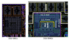
We have been receiving several leaks for Intel's upcoming DG2 GPUs with a 256 Execution Unit model recently appearing on Geekbench paired with a 14-core Alder Lake mobile CPU. The Alder Lake mobile processor featured an integrated Xe GPU with 96 Execution Units which were also benchmarked. The 256 Execution Unit graphics card tested is likely derived from the mid-range DG2-384 GPU. The 96 EU DG2 iGPU featured a maximum frequency of 1.2 GHz while the 256 EU variant increased that to 1.4 GHz. The DG2-256 scored an OpenCL score of 18,450 points in the Geekbench 5 benchmark which places it at GTX 1050 performance level. The DG2-96 integrated GPU scored 6,500 points which is comparable to a GTX 460. While these performance numbers are low it is important to keep in mind that these are just early results from a mid-range mobile offering and Intel is planning to release cards with 512 Execution Units which should compete with the RTX 3070 Ti and 6700 XT.

Intel to Detail "Alder Lake" and "Sapphire Rapids" Microarchitectures at Hot Chips 33, This August

Intel will detail its 12th Gen Core "Alder Lake" client and "Sapphire Rapids" server CPU microarchitectures at the Hot Chips 33 conclave, this August. In fact, Intel's presentation leads the CPU sessions on the opening day of August 23. "Alder Lake" will be the session opener, followed by AMD's presentation of the already-launched "Zen 3," and IBM's 5 GHz Z processor powering its next-gen mainframes. A talk on Xeon "Sapphire Rapids" follows this. Hot Chips is predominantly an engineering conclave, where highly technical sessions are presented by engineers from major semiconductor firms; and so the sessions on "Alder Lake" and "Sapphire Rapids" are expected to be very juicy.

"Alder Lake" is Intel's attempt at changing the PC ecosystem by introducing hybrid CPU cores, a concept introduced to the x86 machine architecture with "Lakefield." The processor will also support next-generation I/O, such as DDR5 memory. The "Sapphire Rapids" server CPU microarchitecture will see an increase in CPU core counts, next-gen I/O such as PCI-Express 5.0, CXL 1.1, DDR5 memory, and more.

CORSAIR Teases DDR5-6400 Memory Coming Later This Year

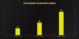
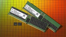
The fifth iteration of DDR technology, called DDR5, is set to arrive later this year. Many makers of DDR4 technology are announcing their plans to switch to the new standard, and CORSAIR is no exception. Known as the maker of high-quality products, CORSAIR has today posted a blog post teasing company's upcoming DDR5 products, and what they will be bringing to the table. For starters, the company has posted data about DDR5 modules that run at 6400 MHz speed, which is assumed to be the speed of the CORSAIR DDR5 modules when they arrive. At such speed, the memory can achieve a bandwidth of 51 GB/s, which is almost double the 26 GB/s that DDR4-3200 MHz memory achieves.

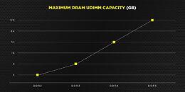
Another point CORSAIR wrote about is the capacity of a single DIMM. With DDR4, the company has made DIMMs that are only up to 32 GB in capacity. However, with DDR5, CORSAIR plans to quadruple that and build a single DDR5 DIMM that has up to 128 GB of memory on it. Another big point was the power required to run the new technology. The DDR4 standard required 1.2 Volts for operation, while the JEDEC specification says that DDR5 needs just 1.1 Volts to run. This will result in a cooler operation of memory modules.

Intel Alder Lake-S Engineering Sample Spotted with DDR5-4800 Memory Running DOTA 2

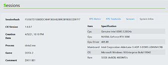
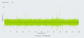
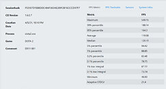
Intel's upcoming Alder Lake-S processors are going to be the company's first attempt at delivering heterogeneous core solutions, combining low-power and high-performance IPs in a single chip. Another important milestone that these processors will reach is DDR5 memory adoption, the first of its kind on consumer platforms. Today, thanks to CapFrameX, a monitoring tool that also hosts a database of benchmark runs, we have a piece of recorded information coming from a test system equipped with an Intel Alder Lake-S processor. The tested system spotted an engineering sample of the Alder Lake-S lineup, clocked at just 2.2 GHz. The core count and core configuration remained unknown.

Alongside the upcoming CPU, the system is composed of NVIDIA's GeForce RTX 3080 GPU and DDR5 memory running at 4800 MHz. There were four sticks present, each having 8 GB capacity. The leaked system was running the DOTA 2 game at an average of 119.98 FPS, which doesn't mean much, given that we don't know which settings were applied and what was the resolution. There is a chart showing the gaming frame rate and frame time, which could be interesting to look at. However, the only new information we have come to know is that the Alder Lake-S is already capable of playing games and the ecosystem support should be very good at launch.

Intel Xe-HPG DG2 GPU Specifications Leak, First GPUs are Coming in H2 2021 in Alder Lake-P Laptops

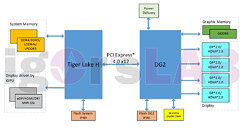
Yesterday, we got information that Intel's upcoming DG2 discrete graphics card is "right around the corner". That means that we are inching closer to the launch of Intel's discrete GPU offerings, and we are going to get another major player in the current GPU market duopoly. Today, however, we are in luck because Igor from Igor's LAB has managed to get ahold of the specifications of Intel's Xe-HPG DG2 graphics card. For starters, it is important to note that DG2 GPU will first come to laptops later this year. More precisely, laptops powered by Alder Lake-P processors will get paired with DG2 discrete GPU in the second half of 2021. The CPU and GPU will connect using the PCIe 4.0 x12 link as shown in the diagram below, where the GPU is paired with the Tiger Lake-H processor. The GPU has its subsystem that handles the IO as well.

Intel "Alder Lake" Memory Controller Could Carry Forward Gear Ratios

Intel's 12th generation Core "Alder Lake" desktop processors could take the concept of memory frequency "gear ratios" forward, according to patch notes from the most recent update to HWInfo64, as reported by Tom's Hardware. Introduced with 11th Gen Rocket Lake, a "gear" ratio is the ratio of the memory clock speed in relation to the memory controller speed. In Gear 1 (or 1:1), the two operate at the same frequency. In Gear 2, the ratio is 1:2 or the memory controller operates at half the frequency of the memory, enabling higher memory overclocking headroom. With "Alder Lake," the company could carry forward this concept for both DDR4 and DDR5 memory types that the controller supports. At this point we don't know if there are just two ratios (Gear 1 and 2), or whether the company could add some more granularity.

Intel Core-1800 Alder Lake Engineering Sample Spotted with 16C/24T Configuration

Intel's upcoming Alder Lake generation of processors is going to be the first iteration of heterogeneous x86 architecture. That means that Intel will for the first time combine smaller, low-power cores, with some big high-performance cores to provide the boost to all the workloads. If a task doesn't need much power, as some background task, for example, the smaller cores are used. And if you need to render something or you want to fire up a game, big cores are used to provide the power needed for the tasks. Intel has decided to provide such an architecture on the advanced 10 nm SuperFin, which represents a major upgrade over the existing 14 nm process.

Today, we got some information from Igor's Lab, showing the leaked specification of the Intel Core-1800 processor engineering sample. While this may not represent the final name, we see that the leaked information shows that the processor is B0 stepping. That means that the CPU will see more changes when the final sample arrives. The CPU has 16 cores with 24 threads. Eight of those cores are big ones with hyperthreading, while the remaining 8 are smaller Atom cores. They are running at the base clock of 1800 MHz, while the boost speeds are 4.6 GHz with two cores, 4.4 GHz with four cores, and 4.2 GHz with 6 cores. When all cores are used, the boost speed is locked at 4.0 GHz. The CPU has a PL1 TDP of 125 Watts, while the PL2 configuration boosts the TDP to 228 Watts. The CPU was reportedly running at 1.3147 Volts during the test. You can check out the complete datasheet below.

AMD Zen 5 "Strix Point" Processors Rumored To Feature big.LITTLE Core Design

AMD launched the 7 nm Zen 3 microarchitecture which powers Ryzen 5000 processors in late 2020, we expect AMD to follow this up with a Zen 3+ on 6 nm later this year and a 5 nm Zen 4 in 2022. We are now beginning to receive the first rumors about the 3 nm Zen 5 architecture which is expected to launch in 2024 in Ryzen 8000 series products. The architecture is reportedly known as "Strix Point" and will be manufactured on TSMC's 3 nm node with a big.LITTLE core design similar to the upcoming Intel Alder Lake and the Apple M1. The Strix Point lineup will consist exclusively of APUs and could feature up to 8 high-performance and 4 low-performance cores which would be less than what Intel plans to offer with Alder Lake. AMD has allegedly already set graphics performance targets for the processors and that they will bring significant changes to the memory subsystem but with rumors for a product 3 years away from launch take them with a healthy dose of skepticism.

CPU-Z Enables Preliminary Support for Intel Alder Lake CPUs

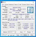
CPU-Z, the CPU monitoring tool used to gather information about the processor your system is running on, has been updated with version 1.96. This new update doesn't change the software much but rather brings support for new hardware. Starting from this revision, Intel's upcoming Alder Lake CPUs have received preliminary support in the tool. To go along with CPUs, the software is now also enabled to recognize Intel's Z6xx motherboards that pair with Alder Lake processors. Alongside that, the software now also brings support for next-generation DDR5 memory, which is supposed to feature speeds anywhere from 4800 to 8400 MT/s. When it comes to AMD, the tool received an update that enables it to read information about AMD's Ryzen 5700G, 5600G, and 5300G APUs, and Radeon RX 6900 XT, 6800 (& XT), 6700 XT GPUs.
Download CPU-Z Version 1.96 Here.

Chinese Company Jiahe Jinwei Begins DDR5 Memory Mass Production

We have seen a number of announcements from key industry players about the introduction of DDR5 memory but today's news from Chinese company Jiahe Jinwei marks the beginning of DDR5 mass production. The company announced that DDR5 RAM from Micron had arrived at its facilities and that memory module production could begin. Jiahe Jinwei is the fourth largest memory manufacturer in China and owns memory brands such as Guangwei and Asgard which have recently announced DDR5 modules with capacities of up to 128 GB and speeds reaching 4,800 MHz. Intel is expected to launch their 12th Generation Alder Lake processors later this year with DDR5 support while AMD will introduce support with Zen 4 processors on a new AM5 socket.

Intel 12th Generation Alder Lake Platform Reportedly Brings 20% Single-Threaded Performance Uplift

Intel only just announced their 11th generation Rocket Lake-S desktop processors last week but we are already receiving information about the next generation Alder Lake-S platform which will finally make the jump to 10 nm. Intel slides for the upcoming family of processors have been leaked and they reveal some interesting information including a claimed 20% single-threaded performance increases from the new Golden Cove core design and 10 nm SuperFin node. The processors will feature Intel Hybrid Technology with a mix of small low-performance cores and large high-performance cores with a maximum of eight each for sixteen total cores. The processors will also include the latest connectivity with both PCIe 4.0 and PCIe 5.0 support along with DDR4 and DDR5 4800 MHz compatibility.

Intel will also be launching a new socket type called LGA1700 with a new package size which will render existing cooling solutions for LGA115X and LGA1200 sockets incompatible. The processors will also come with the launch of a new 600 Series chipset with PCIe 3.0 and PCIe 4.0 support along with the usual complement of USB, SATA, and networking. The entry-level 600-series motherboards will only support DDR4 memory at up to 3200 MHz while high-end Z690 motherboards will include DDR5 support. Intel has confirmed that they intend to launch Alder Lake later this year but it is yet to be known if they are referring to the desktop or mobile series.

DDR5-6400 RAM Benchmarked on Intel Alder Lake Platform, Shows Major Improvement Over DDR4

As the industry is preparing for a shift to the new DDR standard, companies are trying to adopt the new technology and many companies are manufacturing the latest DDR5 memory modules. One of them is Shenzhen Longsys Electronics Co. Ltd, a Chinese manufacturer of memory chips, which has today demonstrated the power of DDR5 technology. Starting with this year, client platforms are expected to make a transition to the new standard, with the data center/server platform following. Using Intel's yet unreleased Alder Lake-S client platform, Longsys has been able to test its DDR5 DIMMs running at an amazing 6400 MHz speed and the company got some very interesting results.

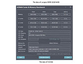
Longsys has demoed a DDR5 module with 32 GB capacity, CAS Latency (CL) of 40 CL, operating voltage of 1.1 V, and memory modules clocked at 6400 MHz. With this being an impressive memory module, this is not the peak of DDR5. According to JEDEC specification, DDR5 will come with up to 8400 MHz speeds and capacities that are up to 128 GB per DIMM. Longsys has run some benchmarks, using an 8-core Alder Lake CPU, in AIDA64 and Ludashi. The company then proceeded to compare these results with DDR4-3200 MHz CL22 memory, which Longsys also manufactures. And the results? In AIDA64 tests, the new DDR5 module is faster anywhere from 12-36%, with the only regression seen in latency, where DDR5 is doubling it. In synthetic Ludashi Master Lu benchmark, the new DDR5 was spotted running 112% faster. Of course, these benchmarks, which you can check out here, are provided by the manufacturer, so you must take them with a grain of salt.

Intel Prepares 19 Alder Lake Processors for Laptops Ranging from 5-55 Watts

As we are getting closer to the launch of Intel's next-generation Alder Lake processors, more information is getting leaked. Today, thanks to the leaked presentation slide, we have some more details regarding Intel's Alder Lake offerings in the laptop sector. As a reminder, Alder Lake uses a hybrid approach to core configuration with the similar mindset Arm's big.LITTLE works. There are a few smaller cores for processing smaller tasks that don't need much power and, of course, there are a few big cores that are used for heavyweight processing as some advanced applications require. The small cores are going to be based on the Gracemont microarchitecture, while the big one will use the Golden Cove design.

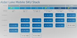
Thanks to @9550pro on Twitter, we have a slide that showcases 19 different Alder Lake configurations for the laptop segment. At the very bottom, there are configurations with a TDP of just five Watts. That is achieved by having just one big, four smaller cores, 48 EU Gen 12 GPU and that is meant for the tablet segment. Going up, we have different ranges depending on the application device, and the highest end is a chip with 55 Watts of power. That model has eight small and eight big cores, combined with 32 EUs of Gen 12 graphics. All models include integrated graphics. The variations of big and small cores have allowed Intel to have as many as 19 different SKUs, that cover every segment needed, by simply balancing the core count. You can check out the rest of the models below for yourself.
Intel Alder Lake Intel Alder Lake Mobile Configurations

Intel "Lunar Lake" Microarchitecture Hits the Radar, Possible "Meteor Lake" Successor

Intel published Linux kernel driver patches that reference a new CPU microarchitecture, codenamed "Lunar Lake." The patch comments refer to "Lunar Lake" as a client platform, and VideoCardz predicts that it could succeed "Meteor Lake." the microarchitecture that follows "Alder Lake," which was recently announced by Intel.

Targeting both mobile and desktop platforms, "Alder Lake" will herald a new 1,700-pin LGA socket for the client desktop, and debut hybrid CPU cores on the form-factor. Expected to be built on a newer silicon fabrication node, such as the 10 nm SuperFin, the chip will combine high-performance "Golden Cove" big cores, with "Gracemont" low-power cores. Its commercial success will determine if Intel continues to take the hybrid-core approach to client processors with future "Meteor Lake" and "Lunar Lake," or whether it will have sorted out its foundry woes and build "Lunar Lake" with a homogeneous CPU core type. With "Alder Lake" expected to debut toward the end of 2021 and "Meteor Lake" [hopefully] by 2022, "Lunar Lake" would only follow by 2023-24.

Intel Alder Lake Processor Tested, Big Cores Ramp Up to 3 GHz

Intel "Alder Lake" is the first processor generation coming from the company to feature the hybrid big.LITTLE type core arrangement and we are wondering how the configurations look like and just how powerful the next-generation processors are going to be. Today, a Geekbench submission has appeared that gave us a little more information about one out of twelve Alder Lake-S configurations. This time, we are getting an 8-core, 16-threaded design with all big cores and no smaller cores present. Such design with no little cores in place is exclusive to the Alder Lake-S desktop platform, and will not come to the Alder Lake-P processors designed for mobile platforms.

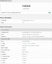
Based on the socket LGA1700, the processor was spotted running all of its eight cores at 2.99 GHz frequency. Please note that this is only an engineering sample and the clock speeds of the final product should be higher. It was paired with the latest DDR5 memory and NVIDIA GeForce RTX 2080 GPU. The OpenCL score this CPU ran has shown that it has provided the GPU with more than enough performance. Typically, the RTX 2080 GPU scores about 106101 points in Geekbench OpenCL tests. Paired with the Alder Lake-S CPU, the GPU has managed to score as much as 108068 points, showing the power of the new generation of cores. While there is still a lot of mystery surrounding the Alder Lake-S series, we have come to know that the big cores used are supposed to be very powerful.

Intel Rocket Lake-S Lands on March 15th, Alder Lake-S Uses Enhanced 10 nm SuperFin Process

In the latest round of rumors, we have today received some really interesting news regarding Intel's upcoming lineup of desktop processors. Thanks to HKEPC media, we have information about the launch date of Intel's Rocket Lake-S processor lineup and Alder Lake-S details. Starting with Rocket Lake, Intel did not unveil the exact availability date on these processors. However, thanks to HKEPC, we have information that Rocket Lake is landing in our hands on March 15th. With 500 series chipsets already launched, consumers are now waiting for the processors to arrive as well, so they can pair their new PCIe 4.0 NVMe SSDs with the latest processor generation.

When it comes to the next generation Alder Lake-S design, Intel is reported to use its enhanced 10 nm SuperFin process for the manufacturing of these processors. This would mean that the node is more efficient than the regular 10 nm SuperFin present on Tiger Lake processors, and some improvements like better frequencies are expected. Alder Lake is expected to make use of big.LITTLE core configuration, with small cores being Gracemont designs, and the big cores being Golden Cove designs. The magic of Golden Cove is expected to result in 20% IPC improvement over Willow Cove, which exists today in Tiger Lake designs. Paired with PCIe 5.0 and DDR5 technology, Alder Lake is looking like a compelling upgrade that is arriving in December of this year. Pictured below is the LGA1700 engineering sample of Alder Lake-S processor.

Intel "Alder Lake-P" Mobile Processor with 14 Cores (6 Big + 8 Little) Geekbenched

An Intel 12th Gen Core "Alder Lake-P" sample surfaced on the Geekbench online results database. The "Alder Lake" microarchitecture introduces heterogenous multi-core to the desktop platform, following its long march from Arm big.LITTLE in 2013, through to laptops with Intel's "Lakefield" in 2019. Intel will build both desktop- and mobile processors using the microarchitecture. The concept is unchanged from big.LITTLE. A processor has two kinds of cores—performance and low-power. Under lower processing loads, the low-power cores are engaged, and the performance cores are only woken up as needed. In theory, this brings about tremendous energy-efficiency gains, as the low-power cores operate within a much higher performance/Watt band than the high-performance cores.

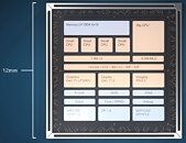
The "Alder Lake" silicon features two kinds of cores—eight "Golden Cove" performance cores, and eight "Gracemont" low-power cores. The "Golden Cove" cores can be configured with HyperThreading (2 logical processors per core). Intel's product managers can create multiple combinations of performance and low-power cores, to achieve total core counts of up to 16, and logical processor counts of up to 24. This also warrants close attention to the composition of the core types, beyond an abstract core-count. A 14-core processor with 6 performance- and 8 low-power cores will perform vastly different from a 14-core processor with 8 performance- and 6 low-power cores. One way to derive core counts is by paying attention to the logical processor (thread) counts, as only the performance "Golden Cove" cores support HTT.
Return to Keyword Browsing
Dec 17th, 2024 22:22 EST change timezone

New Forum Posts

Popular Reviews

Controversial News Posts