News Posts matching #Arcturus

Return to Keyword Browsing

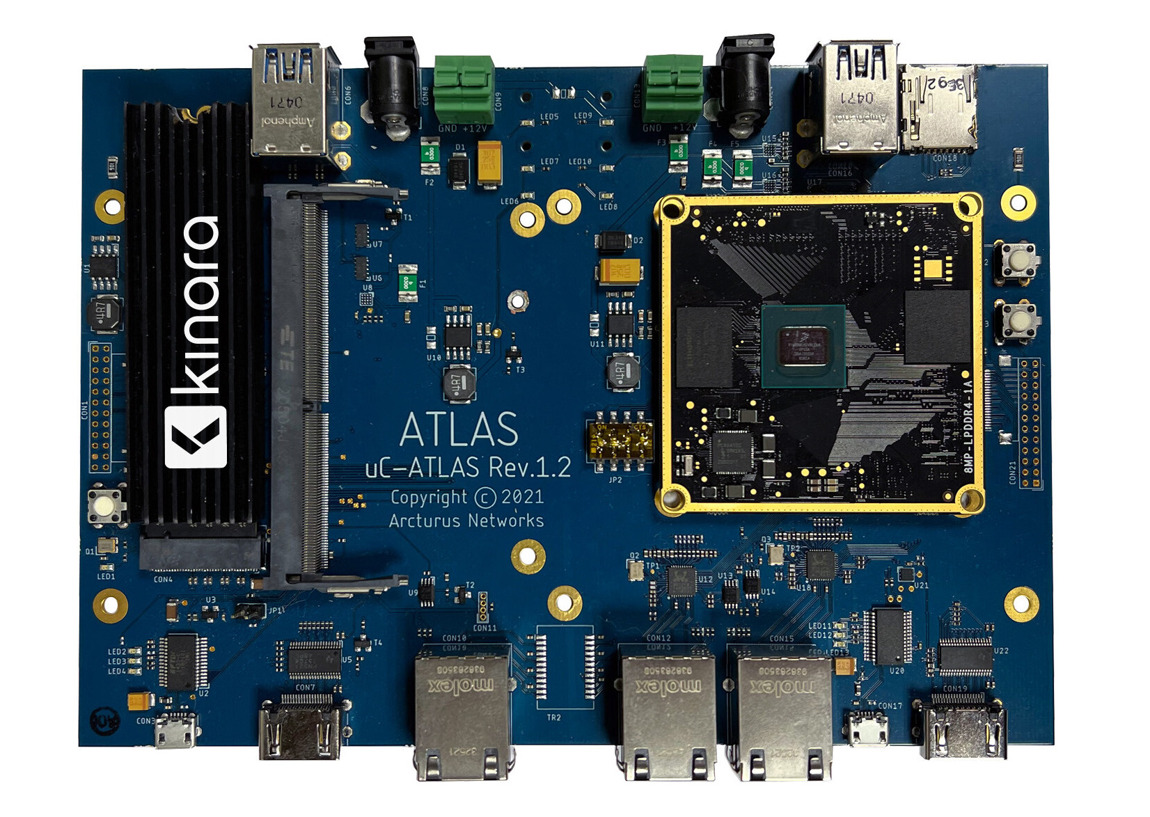
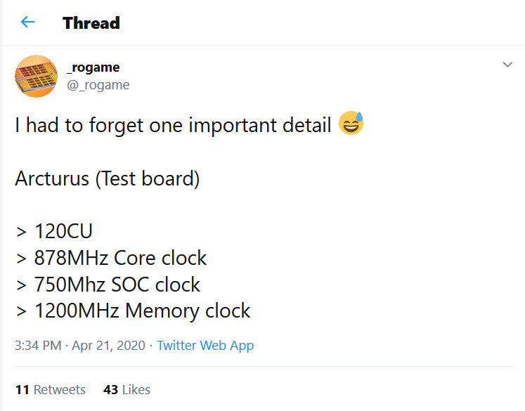
Kinara and Arcturus Partnership to Provide AI Solutions for Smart City and Industry 4.0

Kinara, Inc., developer of unrivaled Edge AI solutions that accelerate and optimize real-time decision making, today announced that it has partnered with Arcturus Networks Inc., provider of edge AI analytics and enablement for smart city applications, to help customers deliver high-performance, cost-optimized AI solutions.

The partnership combines the Kinara Ara-1 Edge AI processor with Arcturus Brinq edge AI and vision analytics software to drive leading-edge detection, tracking and characterization solutions. The partnership delivers the critical software and hardware platforms required by OEMs to build sophisticated real-time edge applications for public safety, transportation, healthcare, retail, and industrial markets. For example, Kinara and Arcturus can deliver a real-time solution for road condition monitoring, allowing public transportation buses retrofitted with smart cameras to detect road obstructions such as potholes and report them directly to city operations.

AMD Radeon MI100 "Arcturus" Alleged Specification Listed, the GPU Could be Coming in December

AMD has been preparing to launch its MI100 accelerator and fight NVIDIA's A100 Ampere GPU in machine learning and AI horizon, and generally compute-intensive workloads. According to some news sources over at AdoredTV, the GPU alleged specifications were listed, along with some slides about the GPU which should be presented at the launch. So to start, this is what we have on the new Radeon MI100 "Arcturus" GPU based on CDNA architecture. The alleged specifications mention that the GPU will feature 120 Compute Units (CUs), meaning that if the GPU keeps the 64-core per CU configuration, we are looking at 7680 cores powered by CDNA architecture.

The leaked slide mentions that the GPU can put out as much as 42 TeraFLOPs of FP32, single-precision compute. This makes it more than twice as fast compared to NVIDIA's A100 GPU at FP32 workloads. To achieve that, the card would need to have all of its 7680 cores running at 2.75 GHz, which would be a bit high number. On the same slide, the GPU is claimed to have 9.5 TeraFLOPs of FP64 dual-precision performance, while the FP16 power is going to be around 150 TeraFLOPs. For comparison, the A100 GPU from NVIDIA features 9.7 TeraFLOPS of FP64, 19.5 TeraFLOPS of FP32, and 312 (or 634 with sparsity enabled) TeraFLOPs of FP16 compute. AMD GPU is allegedly only more powerful for FP32 workloads, where it outperforms the NVIDIA card by 2.4 times. And if that is really the case, AMD has found its niche in the HPC sector, and it plans to dominate there. According to AdoredTV sources, the GPU could be coming in December of this year.

AMD's Next-Generation Radeon Instinct "Arcturus" Test Board Features 120 CUs

AMD is preparing to launch its next-generation of Radeon Instinct GPUs based on the new CDNA architecture designed for enterprise deployments. Thanks to the popular hardware leaker _rogame (@_rogame) we have some information about the configuration of the upcoming Radeon Instinct MI100 "Arcturus" server GPU. Previously, we obtained the BIOS of the Arcturus GPU that showed a configuration of 128 Compute Units (CUs), which resulted in 8,192 of CDNA cores. That configuration had a specific setup of 1334 MHz GPU clock, SoC frequency of 1091 MHz, and memory speed of 1000 MHz. However, there was another GPU test board spotted which featured a bit different specification.

The reported configuration is an Arcturus GPU with 120 CUs, resulting in a CDNA core count of 7,680 cores. These cores are running at frequencies of 878 MHz for the core clock, 750 MHz SoC clock, and a surprising 1200 MHz memory clock. While the SoC and core clocks are lower than the previous report, along with the CU count, the memory clock is up by 200 MHz. It is important to note that this is just a test board/variation of the MI100, and actual frequencies should be different.
AMD Radeon Instinct MI60

AMD Radeon Instinct MI100 "Arcturus" Hits the Radar, We Have its BIOS

AMD's upcoming large post-Navi graphics chip, codenamed "Arcturus," will debut as "Radeon Instinct MI100", which is an AI-ML accelerator under the Radeon Instinct brand, which AMD calls "Server Accelerators." TechPowerUp accessed its BIOS, which is now up on our VGA BIOS database. The card goes with the device ID "0x1002 0x738C," which confirms "AMD" and "Arcturus,". The BIOS also confirms that memory size is at a massive 32 GB HBM2, clocked at 1000 MHz real (possibly 1 TB/s bandwidth, if memory bus width is 4096-bit).

Both Samsung (KHA884901X) and Hynix memory (H5VR64ESA8H) is supported, which is an important capability for AMD's supply chain. From the ID string "MI100 D34303 A1 XL 200W 32GB 1000m" we can derive that the TDP limit is set to a surprisingly low 200 W, especially considering this is a 128 CU / 8,192 shader count design. Vega 64 and Radeon Instinct MI60 for comparison have around 300 W power budget with 4,096 shaders, 5700 XT has 225 W with 2560 shaders, so either AMD achieved some monumental efficiency improvements with Arcturus or the whole design is intentionally running constrained, so that AMD doesn't reveal their hand to these partners, doing early testing of the card.

AMD "Navi" GPU Architecture Successor Codenamed "Arcturus"?

Arcturus is the fourth brightest star in the night sky, and could be the a new GPU architecture by AMD succeeding "Navi," according to a Phoronix report. The codename of Navi-successor has long eluded AMD's roadmap slides. The name "Arcturis" surfaced on Phoronix community forums, from a post by an AMD Linux liaison who is a member there. The codename is also supported by the fact that AMD is naming its GPU architectures after the brightest stars in the sky (albeit in a descending order of their brightness). Polaris is the brightest, followed by Vega, Navi, and Arcturus.

AMD last referenced the Navi-successor on a roadmap slide during its 2017 Financial Analyst Day presentation by Mark Papermaster. That slide mentioned "Vega" to be built on two silicon fabrication processes, 14 nm and "14 nm+." We know now that AMD intends to build a better-endowed "Vega" chip on 7 nm, which could be the world's first 7 nm GPU. "Navi" is slated to be built on 7 nm as the process becomes more prevalent in the industry. The same slide mentions Navi-successor as being built on "7 nm+," which going by convention, could refer to an even more advanced process than 7 nm. Unfortunately, even in 2017, when the industry was a touch more optimistic about 7 nm, AMD expected the Navi-successor to only come out by 2020. We're not holding our breath.
Return to Keyword Browsing
Jul 16th, 2024 06:27 EDT change timezone

New Forum Posts

Popular Reviews

Controversial News Posts