Samsung Mass Producing Industry's Most Advanced 4 Gb DDR3, Using 20 nm Process
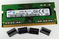
Samsung Electronics Co., Ltd., the world leader in memory technology, today announced that it is mass producing the most advanced DDR3 memory, based on a new 20 nanometer process technology, for use in a wide range of computing applications. Samsung has pushed the envelope of DRAM scaling, while utilizing currently available immersion ArF lithography, in its roll-out of the industry's most advanced 20-nanometer (nm) 4-gigabit (Gb) DDR3 DRAM.
With DRAM memory, where each cell consists of a capacitor and a transistor linked to one another, scaling is more difficult than with NAND Flash memory in which a cell only needs a transistor. To continue scaling for more advanced DRAM, Samsung refined its design and manufacturing technologies and came up with a modified double patterning and atomic layer deposition.
With DRAM memory, where each cell consists of a capacitor and a transistor linked to one another, scaling is more difficult than with NAND Flash memory in which a cell only needs a transistor. To continue scaling for more advanced DRAM, Samsung refined its design and manufacturing technologies and came up with a modified double patterning and atomic layer deposition.
