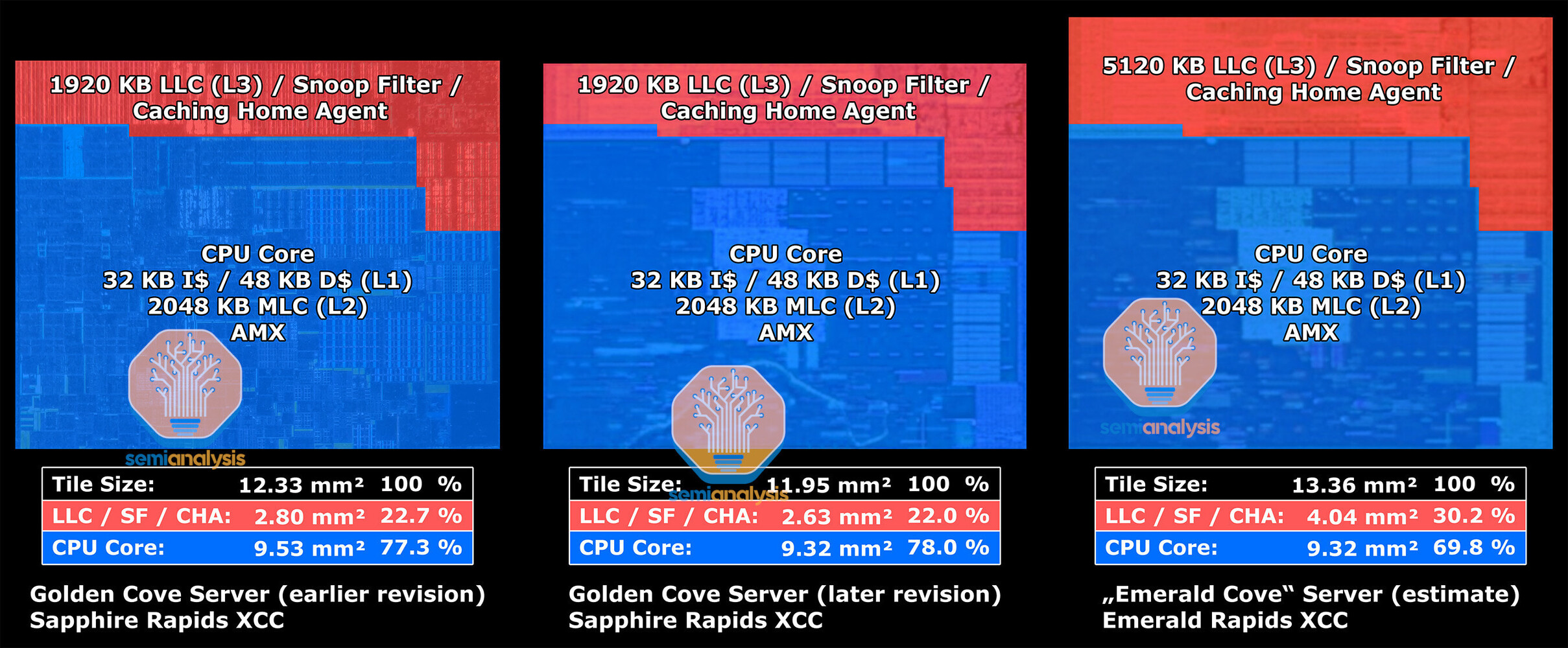
Intel Details EMIB-T Advanced Packaging for HBM4 and UCIe
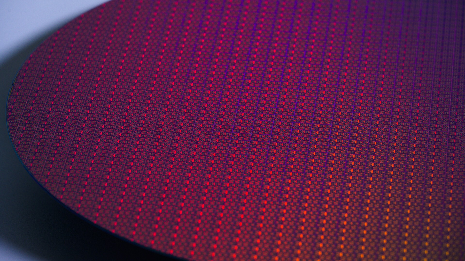
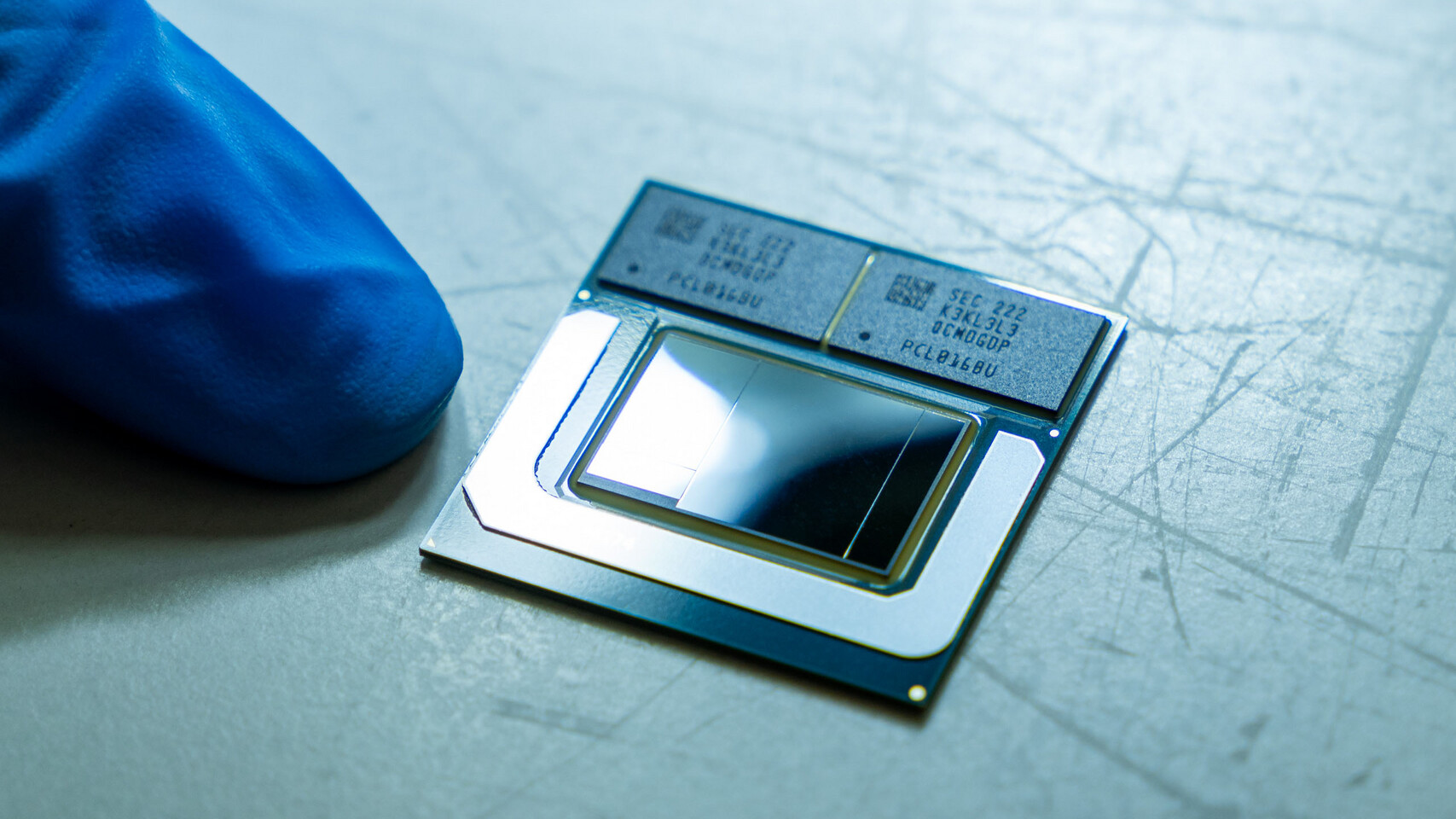
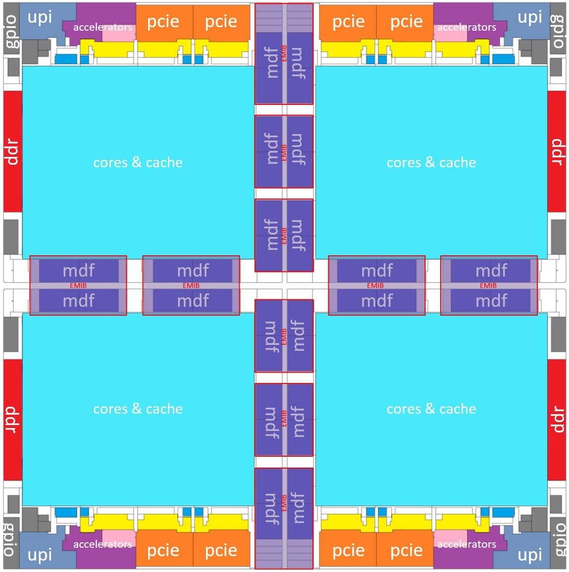
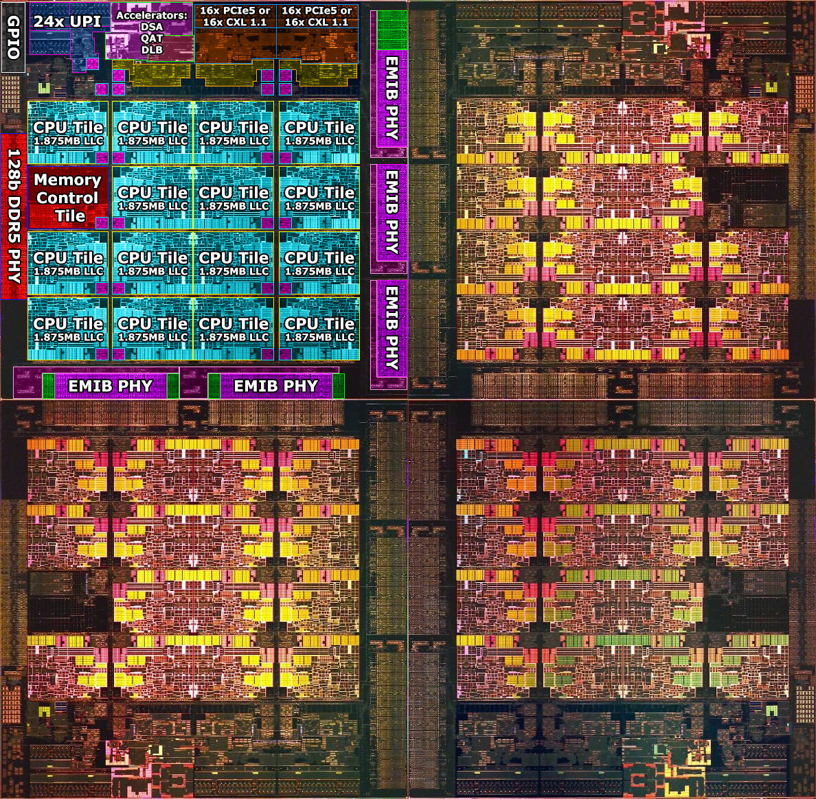
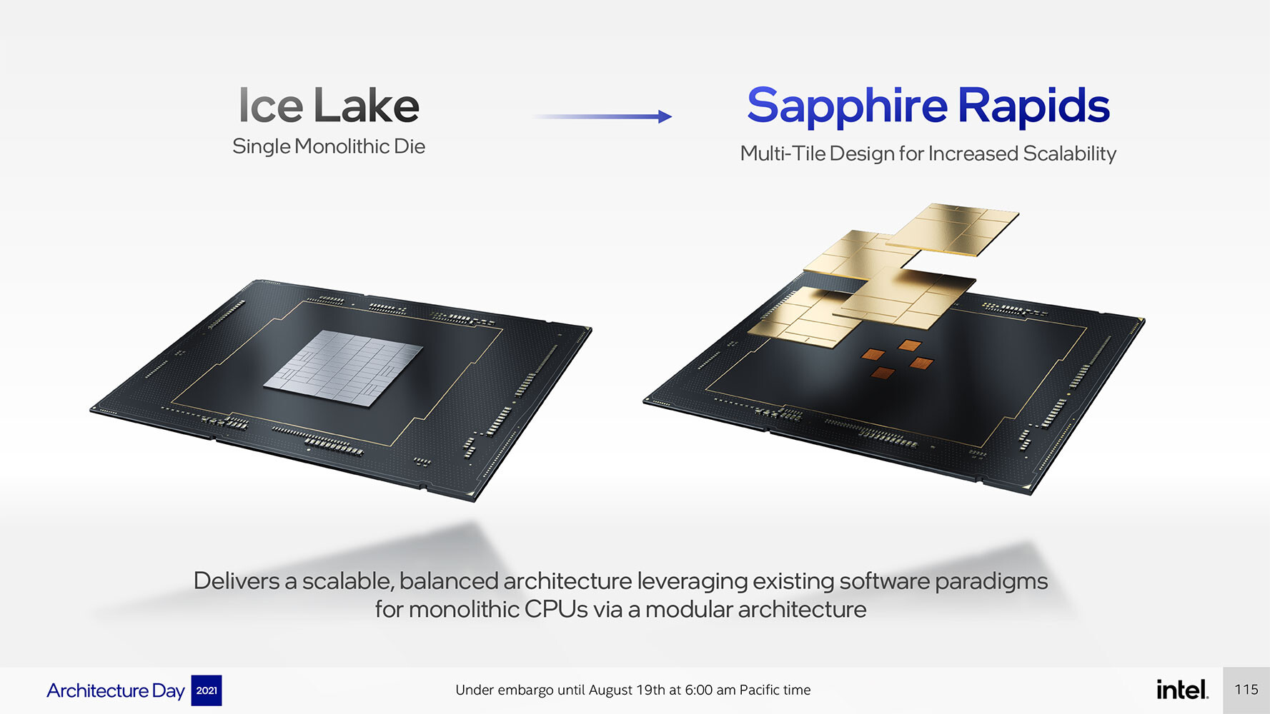
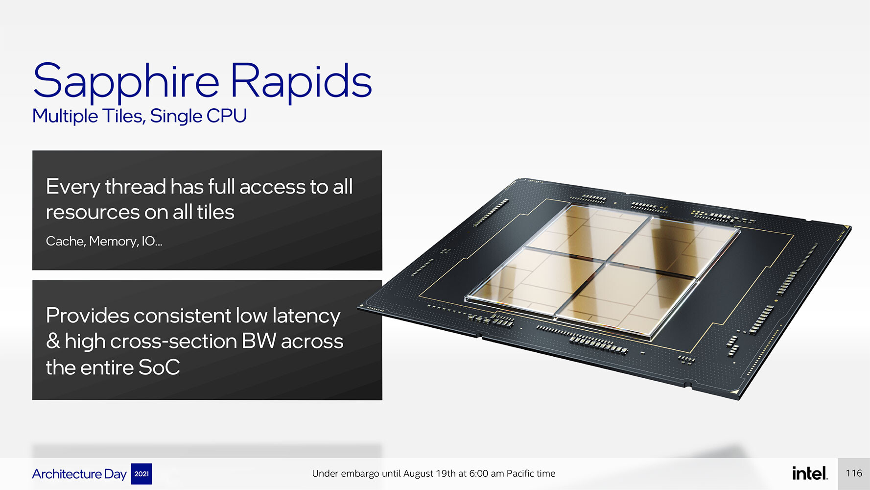
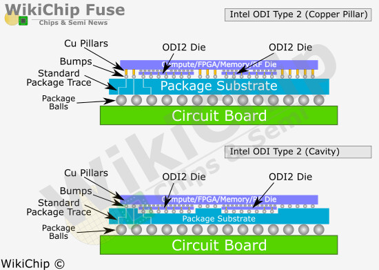
This week at the Electronic Components Technology Conference (ECTC), Intel introduced EMIB-T, an important upgrade to its embedded multi-die interconnect bridge packaging. First showcased at the Intel Foundry Direct Connect 2025 event, EMIB-T incorporates through-silicon vias (TSVs) and high-power metal-insulator-metal capacitors into the existing EMIB structure. According to Dr. Rahul Manepalli, Intel Fellow and vice president of Substrate Packaging Development, these changes allow a more reliable power supply and stronger communication between separate chiplets. Conventional EMIB designs have struggled with voltage drops because of their cantilevered power delivery paths. In contrast, EMIB-T routes power directly through TSVs from the package substrate to each chiplet connection. The integrated capacitors compensate for fast voltage fluctuations and preserve signal integrity.
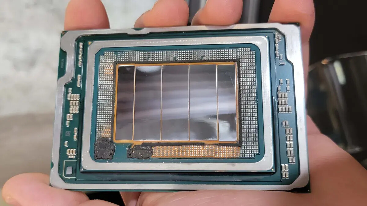
This improvement will be critical for next-generation memory, such as HBM4 and HBM4e, where data rates of 32 Gb/s per pin or more are expected over a UCIe interface. Intel has confirmed that the first EMIB-T packages will match the current energy efficiency of around 0.25 picojoules per bit while offering higher interconnect density. The company plans to reduce the bump pitch below today's standard of 45 micrometers. Beginning in 2026, Intel intends to produce EMIB-based packages measuring 120 by 120 millimeters, roughly eight times the size of a single reticle. These large substrates could integrate up to twelve stacks of high-bandwidth memory alongside multiple compute chiplets, all connected by more than twenty EMIB bridges. Looking further ahead, Intel expects to push package dimensions to 120 by 180 millimeters by 2028. Such designs could accommodate more than 24 memory stacks, eight compute chiplets, and 38 or more EMIB bridges. These developments closely mirror similar plans announced by TSMC for its CoWoS technology. In addition to EMIB-T, Intel also presented a redesigned heat spreader that reduces voids in the thermal interface material by approximately 25%, as well as a new thermal-compression bonding process that minimizes warping in large package substrates.

This improvement will be critical for next-generation memory, such as HBM4 and HBM4e, where data rates of 32 Gb/s per pin or more are expected over a UCIe interface. Intel has confirmed that the first EMIB-T packages will match the current energy efficiency of around 0.25 picojoules per bit while offering higher interconnect density. The company plans to reduce the bump pitch below today's standard of 45 micrometers. Beginning in 2026, Intel intends to produce EMIB-based packages measuring 120 by 120 millimeters, roughly eight times the size of a single reticle. These large substrates could integrate up to twelve stacks of high-bandwidth memory alongside multiple compute chiplets, all connected by more than twenty EMIB bridges. Looking further ahead, Intel expects to push package dimensions to 120 by 180 millimeters by 2028. Such designs could accommodate more than 24 memory stacks, eight compute chiplets, and 38 or more EMIB bridges. These developments closely mirror similar plans announced by TSMC for its CoWoS technology. In addition to EMIB-T, Intel also presented a redesigned heat spreader that reduces voids in the thermal interface material by approximately 25%, as well as a new thermal-compression bonding process that minimizes warping in large package substrates.