News Posts matching #GCN

Return to Keyword Browsing

AMD Unveils GPU Architecture Roadmap, "Polaris" to Skip HBM2 Memory?

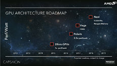
Alongside its big Radeon Pro Duo flagship graphics card launch, AMD unveiled its GPU architecture roadmap that looks as far into the future as early-2018. By then, AMD will have launched as many as three new GPU architectures. It begins with the launch of its 4th generation Graphics CoreNext architecture, codenamed "Polaris," in mid-2016. Built on the 14 nm FinFET process, "Polaris" is expected to offer a whopping 2.5x increase in performance-per-Watt for AMD, compared to its current GCN 1.2 architecture on 28 nm.

Hot on Polaris' heels, in early-2017, AMD plans to launch the "Vega" GPU architecture. While this appears to offer a 50% increase in performance-per-Watt over Polaris, its highlight is HBM2 memory. Does this mean that AMD plans to skip HBM2 on Polaris, and stick to GDDR5X? Could AMD be opting for a similar approach to NVIDIA, by launching its performance-segment GPU first as an enthusiast product, giving it a free run on the markets till early-2017, and then launching a Vega-based big-chip with HBM2 memory, taking over as the enthusiast-segment product? Some time in early-2018, AMD will launch the "Navi" architecture, which appears to offer a 2.5x performance-per-Watt lead over Polaris, taking advantage of an even newer memory standard.

AMD Working on a "Polaris" Chip with 232 mm² Die Area

A former AMD employee who was with the company till July 2015, disclosed vague details of the various chip projects he was involved in. Two of those projects, labeled "A" and "B" were core-logic (southbridge). Project "F" drew the attention of the press to a graphics chip with a die-area of 232 mm², 430 function blocks, built on the 14 nm LPP process. A function block can be any differentiated or unique structure on a silicon die. 3DCenter speculates that this could be a GPU based on the company's upcoming "Polaris" (GCN 4.0) architecture; and likely a performance-segment chip from the next-gen GPU family.

AMD Working on Two "Polaris" GPUs: Raja Koduri

AMD Radeon Technologies Group (RTG) head Raja Koduri, in an interview with Venture Beat, confirmed that the company is currently working on two 14 nm FinFET GPUs based on the "Polaris" (4th generation Graphics CoreNext) architecture. He was quoted as referring to the two chips as "Polaris 10" and "Polaris 11." He remarked that the two chips are "extremely power efficient."

Koduri ran Venture Beat through what's new with these chips, besides being built on the 14 nm process and GCN 4.0 stream processors - a redesigned front-end, new geometry processors, a new multimedia engine, and new display controllers. GCN 4.0 lends the chip an up-to-date API support besides significantly higher performance, the new multimedia engine features native h.265 hardware acceleration, and the display controllers support the latest DisplayPort 1.3 and HDMI 2.0a connectors.

AMD Demonstrates Revolutionary 14 nm FinFET Polaris GPU Architecture

AMD provided customers with a glimpse of its upcoming 2016 Polaris GPU architecture, highlighting a wide range of significant architectural improvements including HDR monitor support, and industry-leading performance-per-watt. AMD expects shipments of Polaris architecture-based GPUs to begin in mid-2016.

AMD's Polaris architecture-based 14nm FinFET GPUs deliver a remarkable generational jump in power efficiency. Polaris-based GPUs are designed for fluid frame rates in graphics, gaming, VR and multimedia applications running on compelling small form-factor thin and light computer designs.

"Our new Polaris architecture showcases significant advances in performance, power efficiency and features," said Lisa Su, president and CEO, AMD. "2016 will be a very exciting year for Radeon fans driven by our Polaris architecture, Radeon Software Crimson Edition and a host of other innovations in the pipeline from our Radeon Technologies Group."

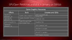
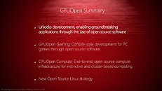
AMD Counters GameWorks with GPUOpen, Leverages Open-Source

AMD is in no mood to let NVIDIA run away with the PC graphics market, with its GameWorks SDK that speeds up PC graphics development (in turn increasing NVIDIA's influence over the game development, in a predominantly AMD GCN driven client base (20% PC graphics market-share, and 100% game console market share). AMD's counter to GameWorks is GPUOpen, with the "open" referring to "open-source."

GPUOpen is a vast set of pre-developed visual-effects, tools, libraries, and SDKs, designed to give developers "unprecedented control" over the GPU, helping them get their software closer to the metal than any other software can. The idea here is that an NVIDIA GameWorks designed title won't get you as "close" to the metal on machines such as the Xbox One and PlayStation 4, or PCs with Radeon GPUs, as GPUOpen. Getting "close to the metal" is defined as directly leveraging features exposed by the GPU, with as few software layers between the app and the hardware as possible.

AMD Announces Radeon Crimson Software

AMD today released its completely reimagined graphics software suite, Radeon Software Crimson Edition, giving users an exceptional new user experience, 12 new or enhanced features, up to 20 percent more graphics performance, adjustability that can nearly double generational energy efficiency2, and rock-solid stability across the full spectrum of AMD graphics products. The release is the first from the Radeon Technologies Group, which recently announced a renewed focus on software placing it on par with hardware initiatives.

"As the primary way that people interact with our products, our software deserves to be viewed as a top priority, and going forward that's exactly what we're doing, delivering easy-to-use software that is packed with real user benefits, starting with Radeon Software Crimson Edition," said Raja Koduri, senior vice president and chief architect, Radeon Technologies Group. "Radeon Technologies Group is laser-focused on the vertical integration of all things graphics, propelling the industry forward by driving performance per watt, creating innovative technologies and ensuring that the software supporting our GPUs is world class."
DOWNLOAD: AMD Radeon Software Crimson Edition for Windows 10 64-bit | Windows 10 32-bit | Windows 8.1 64-bit | Windows 8.1 32-bit | Windows 7 64-bit | Windows 7 32-bit

AMD Announces the Radeon R9 380X Graphics Card

AMD announced the Radeon R9 380X graphics card. Positioned between the Radeon R9 380 and the R9 390, this card starts at US $229, and takes advantage of a huge gap in NVIDIA's lineup, between the GeForce GTX 960 ($190) and the GTX 970 ($319). Based on the 28 nm "Antigua" ("Tonga") silicon, this SKU features the full complement of the chip's 32 Graphics CoreNext (GCN) compute units, amounting to 2,048 stream processors. It also features 128 TMUs, 32 ROPs, and a 256-bit wide GDDR5 memory interface, holding 4 GB of memory. The core is clocked at 970 MHz, and the memory at 5.70 GHz (GDDR5-effective), amounting to a memory bandwidth of 182 GB/s.
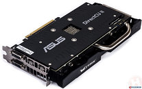
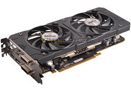
Three AIB Branded Radeon R9 380X Graphics Cards Pictured

Here are the first pictures of three AIB-branded Radeon R9 380X graphics cards, including one each from ASUS, XFX, and GIGABYTE. The ASUS branded Radeon R9 380X graphics card, the R9 380X STRIX, features the company's dual-slot, dual-fan DirectCU II cooling solution. ASUS is also giving it a slick back-plate, and offering it in two variants based on factory-overclock (or lack of it).

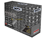
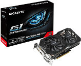
The XFX branded R9 380X features a similar product size to the ASUS card, featuring a moderately long PCB, and a dual-slot, dual-fan "Double Dissipation" cooler. XFX will sell variants of this card in reference and factory-overclocked speeds. Lastly, there's GIGABYTE. Like the others, this card features a medium-size PCB, with the company's dual-slot WindForce 2X cooling solution. Based on the 28 nm "Tonga" aka "Antigua" silicon, the R9 380X reportedly features 2,048 GCN 1.2 stream processors, 128 TMUs, 32 ROPs, and a 256-bit wide GDDR5 memory interface, holding 4 GB of memory. It's expected to launch later this week.
Souces: VideoCardz, HardwareInfo, WCCFTech

AMD "Fiji" GPU Die-shot Revealed by Chipworks

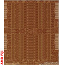
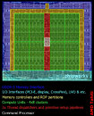
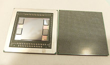
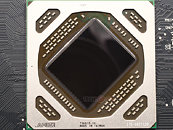
VLSI technical publication Chipworks posted the first clear die-shot of AMD's "Fiji" silicon, revealing intricate details of the most technically advanced GPU. What makes Fiji the most advanced graphics chip is its silicon interposer and stacked HBM chips making up a multi-chip module. It's the die in the center of all that, which went under Chipworks' microscope.

The die-shot reveals a component layout that's more or less an upscale of "Tonga." Some of the components, such as the front-end appear to be entirely identical to "Tahiti" or "Tonga." The shot reveals the 64 GCN compute units arranged in four rows, on either side of the central portion with the dispatch and primitive setup pipelines. The pad-area of the on-die memory controllers appear to be less than the large memory I/O pads that made up the 384-bit interface of "Tahiti." The first picture below is the die-shot of "Fiji," followed by a color-coded die-shot of "Tahiti."

AMD Pro A12 "Carrizo" Chip Offers TDP as Low as 12W

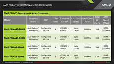
AMD's "Excavator" module could fetch big power dividends for the company, with the top of the line Pro A12 "Carrizo" APU for mobile platforms offering TDP as low as 12W (normal usage), going up to 35W (maximum stress). AMD allows users to set the TDP for their processors. Built on the existing 28 nm process, these chips offer TDPs as low as the ones offered by Intel, built on 22 nm and even 14 nm nodes.

This is made possible because "Excavator" features heavily compacted registers and decode engines, and AMD spent a lot of R&D kicking out redundant or useless components from the silicon. The recently launched A-Series Pro "Carrizo" APUs feature two "Excavator" modules (four CPU cores), a GPU with eight GCN 1.2 compute units (512 stream processors), 2 MB of total cache, dual-channel DDR3-2133 integrated memory controllers.

NVIDIA "Pascal" GPUs to be Built on 16 nm TSMC FinFET Node

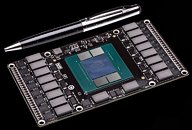
NVIDIA's next-generation GPUs, based on the company's "Pascal" architecture, will be reportedly built on the 16 nanometer FinFET node at TSMC, and not the previously reported 14 nm FinFET node at Samsung. Talks of foundry partnership between NVIDIA and Samsung didn't succeed, and the GPU maker decided to revert to TSMC. The "Pascal" family of GPUs will see NVIDIA adopt HBM2 (high-bandwidth memory 2), with stacked DRAM chips sitting alongside the GPU die, on a multi-chip module, similar to AMD's pioneering "Fiji" GPU. Rival AMD, on the other hand, could build its next-generation GCNxt GPUs on 14 nm FinFET process being refined by GlobalFoundries.

PowerColor Launches its Radeon R9 Nano Graphics Card

TUL Corporation, a leading and innovative manufacturer of AMD graphic cards since 1997, has proudly announced a new graphics card that is powered by the world's most advanced and innovative GPU. The PowerColor R9 Nano 4GB HBM delivers revolutionary innovation, power efficiency, performance, and enables a new paradigm for small form factor PCs. The PowerColor R9 Nano 4GB HBM is the first GPU with on-chip High Bandwidth Memory (HBM) delivering extreme 4K gaming performance in an incredibly innovative 6-inch length graphics card.
Even though the size of PowerColor R9 Nano graphics card is only just 6 inches in length, it gives a radical leap forward in enthusiast class performance that features to an inventive design no equal for the Mini-ITX PC. No graphics card has ever packed so much performance and power into such a small form factor. The PowerColor R9 Nano is armed with the first-ever GPU with High-Bandwidth Memory (HBM) integrated on-chip that delivers more than 4 times the bandwidth per watt over GDDR5. Add that along with a 4096-bit memory interface for incredible new advances in power and efficiency which makes the most innovative total solution GPU available today.

PowerColor Launches Radeon R9 390 X2 Devil13 Dual-GPU Graphics Card

TUL Corporation, a leading and innovative manufacturer of AMD graphic cards since 1997, has proudly announced a new and most powerful graphics card in the world among AMD Radeon R9 390 series. The PowerColor Devil 13 Dual Core R9 390 is packed with dual GRENADA core, designed to tackle the most demanding high end gaming titles on the market. It utilizes 16 GB of GDDR5 memory with a core clock speed at 1000 MHz, and 1350 MHz for memory clock speed which is connected via a new high speed 1024-bit (512-bit x2) memory interface.

PowerColor Devil 13 Dual Core R9 390 is built with carefully-designed Platinum Power Kit and ultra-efficient thermal design. It consists of massive 15-phase power delivery, PowerIRstage, Super Cap and Ferrite Core Choke that provides the stability and reliability for such high-end graphics solution. To support maximum performance and to qualify for the Devil 13 cooling system, 3 Double Blades Fans are attached on top of the enormous surface of aluminum fins heatsink connected with total of 10 pieces of heat pipes and 2 pieces of large die-cast panels. This superb cooling solution achieves a perfect balance between thermal solution and noise reduction. The PowerColor Devil 13 Dual Core R9 390 has the LED backlighting that glows a bright red color, pulsating slowly on the Devil 13 logo.

Lack of Async Compute on Maxwell Makes AMD GCN Better Prepared for DirectX 12

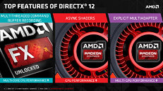
It turns out that NVIDIA's "Maxwell" architecture has an Achilles' heel after all, which tilts the scales in favor of competing AMD Graphics CoreNext architecture, in being better prepared for DirectX 12. "Maxwell" lacks support for async compute, one of the three highlight features of Direct3D 12, even as the GeForce driver "exposes" the feature's presence to apps. This came to light when game developer Oxide Games alleged that it was pressured by NVIDIA's marketing department to remove certain features in its "Ashes of the Singularity" DirectX 12 benchmark.

Async Compute is a standardized API-level feature added to Direct3D by Microsoft, which allows an app to better exploit the number-crunching resources of a GPU, by breaking down its graphics rendering tasks. Since NVIDIA driver tells apps that "Maxwell" GPUs supports it, Oxide Games simply created its benchmark with async compute support, but when it attempted to use it on Maxwell, it was an "unmitigated disaster." During to course of its developer correspondence with NVIDIA to try and fix this issue, it learned that "Maxwell" doesn't really support async compute at the bare-metal level, and that NVIDIA driver bluffs its support to apps. NVIDIA instead started pressuring Oxide to remove parts of its code that use async compute altogether, it alleges.

AMD Showcases Graphics, Energy Efficient Computing and Die-Stacking Innovation

Top technologists from AMD are detailing the engineering accomplishments behind the performance and energy efficiency of the new high-performance Accelerated Processing Unit (APU), codenamed "Carrizo," and the new AMD Radeon R9 Fury family of GPUs, codenamed "Fiji," at the prestigious annual Hot Chips symposium starting today. The presentations will focus on new details of the high-definition video and graphics processing engines on the 6th Generation AMD A-Series APU ("Carrizo"), and the eight year journey leading to die-stacking technology and all-new memory architecture included on the latest top-of-the-line AMD Radeon Fury Series GPUs ("Fiji") for 4K gaming and VR. Using a true System-on-Chip (SoC) design, 6th Generation AMD A-Series processors are designed to reduce the power consumed by the x86 cores alone by 40 percent, while providing substantial gains in CPU, graphics, and multimedia performance versus the prior generation APU. The new AMD Radeon R9 Fury X GPU achieves up to 1.5x the performance-per-watt of the previous high-end GPU from AMD.

"With our new generation of APU and GPU technology, our engineering teams left no stone unturned for performance and energy efficiency," said Mark Papermaster, chief technology officer at AMD. "Using innovative design for our APUs, we've vastly increased the number of transistors on-chip to increase functionality and performance, implemented advanced power management, and completed the hardware implementation of Heterogeneous System Architecture. For our latest GPUs, AMD is the first to introduce breakthrough technology in the form of die-stacking and High-Bandwidth Memory. The results are great products with very large generational performance-per-watt gains."

PowerColor Announces the DEVIL Radeon R9 390X Graphics Card

TUL Corporation, a leading and innovative manufacturer of AMD graphics cards since 1997, has released the Devil R9 390X 8GB GDDR5. It is based on the latest GCN architecture to help deliver outstanding and extraordinary graphics performance and image quality.

Devil R9 390X utilizes 8GB of GDDR5 memory, 2816 stream processors, comes with a core clock speed at 1100MHz, and 1525MHz memory clock speed which is connected via a new high speed 512-bit memory interface. For enhancing power efficiency and preventing losses, Digital PWM solution is provided to work at a higher frequency in order to support fine tuning adjustment and low ripple at an output voltage. Moreover, the total of 8 phases (6+1+1) board design is applied to the product for power efficiency, stability, and delivering ultimate performance at OC mode. PowIRstage increases the power up to 3-13%, features up to 1.0 MHz switching frequency, and supports efficient cooling ability. This model supports Direct 12 and AMD's newest technologies such as Virtual Super Resolution, FreeSync, Liquid VR, and 4K resolution.

Google Chooses Vulkan as the 3D Graphics API for Android

Google announced that it chose Vulkan, the next-generation, cross-platform 3D graphics API from Khronos, the people behind OpenGL; as the default API for upcoming versions of its Android operating-system. It currently uses OpenGL ES. GL-ES is widely supported across several embedded platforms, with its most recent update, GL ES 3.2, being released as recently as last week. What makes Khronos particularly interesting is that it's heavily based on AMD Mantle, a low-overhead API that proved its chops against DirectX 11 on the PC platform, before being withdrawn by AMD, in favor of DirectX 12.

Google will be helping developers through the transition between OpenGL ES and Vulkan using a suite of documentation, SDKs rich in compatibility test suits, and more. Vulkan's march to the PC could be a lot less straightforward. It's still being seen as rebranded Mantle, and while AMD announced support for all its Graphics CoreNext GPUs, there's no such announcement from NVIDIA. It could see good adoption with Apple's Mac OS, and desktop *nix. Vulkan could see a lot of popularity with game consoles other than Microsoft Xbox. Sony PlayStation 4, and Nintendo's upcoming console, which use AMD GCN GPUs, could take advantage of Vulkan, due to its lower CPU overhead and close-to-metal optimizations, compared to OpenGL.
AMD Announces the Radeon R9 Fury Graphics Card

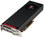
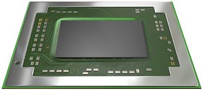
AMD announced the second graphics card based on its swanky new "Fiji" silicon, the Radeon R9 Fury. Positioned between the R9 390X and the R9 Fury X, this card offers higher pixel-crunching muscle than the R9 390X, while giving you cutting-edge 4 GB HBM memory. It can play any game at 2560 x 1440, and at Ultra HD (3840 x 2160), with reasonable eye-candy. The R9 Fury is designed solely for AMD's AIB partners to come up with their own air-cooled products.

AMD carved the R9 Fury out of the Fiji silicon, by enabling 56 of the 64 GCN compute units physically present, yielding 3,584 stream processors. Other specifications include 224 TMUs, 64 ROPs, and 4 GB of memory across a 4096-bit wide HBM interface. The core is clocked at 1000 MHz, and the memory at 500 MHz (512 GB/s). Custom-design boards will offer factory-overclocked speeds. AMD is pricing the R9 Fury at US $549.

AMD Announces FirePro S9170 32GB GPU Compute Card

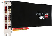
AMD today announced the new AMD FirePro S9170 server GPU, the world's first and fastest 32GB single-GPU server card for DGEMM heavy double-precision workloads, with support for OpenCL 2.0. Based on the second-generation AMD Graphics Core Next (GCN) GPU architecture, this new addition to the AMD FirePro server GPU family is capable of delivering up to 5.24 TFLOPS of peak single precision compute performance while enabling full throughput double precision performance, providing up to 2.62 TFLOPS of peak double precision performance. Designed with compute-intensive workflows in mind, the AMD FirePro S9170 server GPU is ideal for data center managers who oversee clusters within academic or government bodies, oil and gas industries, or deep neural network compute cluster development.

"AMD is recognized as an HPC industry innovator as the graphics provider with the top spot on the November 2014 Green500 List. Today the best GPU for compute just got better with the introduction of the AMD FirePro S9170 server GPU to complement AMD's impressive array of server graphics offerings for high performance compute environments," said Sean Burke, corporate vice president and general manager, AMD Professional Graphics group. "The AMD FirePro S9170 server GPU can accelerate complex workloads in scientific computing, data analytics, or seismic processing, wielding an industry-leading 32GB of memory. We designed the new offering for supercomputers to achieve massive compute performance while maximizing available power budgets."

AMD "Fiji" Block Diagram Revealed, Runs Cool and Quiet

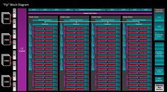
AMD's upcoming flagship GPU silicon, codenamed "Fiji," which is breaking ground on new technologies, such as HBM, memory-on-package, a specialized substrate layer that connects the GPU with it, called Interposer; features a hefty feature-set. More on the "Fiji" package and its memory implementation, in our older article. Its block diagram (manufacturer-drawn graphic showing the GPU's component hierarchy), reveals a scaling up, of the company's high-end GPU launches over the past few years.

"Fiji" retains the quad Shader Engine layout of "Hawaii," but packs 16 GCN Compute Units (CUs), per Shader Engine (compared to 11 CUs per engine on Hawaii). This works out to a stream processor count of 4,096. Fiji is expected to feature a newer version of the Graphics CoreNext architecture than "Hawaii." The TMU count is proportionately increased, to 256 (compared to 176 on "Hawaii"). AMD doesn't appear to have increased the ROP count, which is still at 64. The most significant change, however, is its 4096-bit HBM memory interface, compared to 512-bit GDDR5 on "Hawaii."

NVIDIA Could Capitalize on AMD Graphics CoreNext Not Supporting Direct3D 12_1

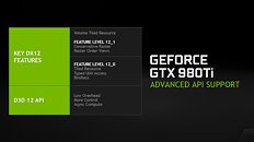
AMD's Graphics CoreNext (GCN) architecture does not support Direct3D feature-level 12_1 (DirectX 12.1), according to a ComputerBase.de report. The architecture only supports Direct3D up to feature-level 12_0. Feature-level 12_1 adds three features over 12_0, namely Volume-Tiled Resources, Conservative Rasterization and Rasterizer Ordered Views.

Volume Tiled-resources, is an evolution of tiled-resources (analogous to OpenGL mega-texture), in which the GPU seeks and loads only those portions of a large texture that are relevant to the scene it's rendering, rather than loading the entire texture to the memory. Think of it as a virtual memory system for textures. This greatly reduces video memory usage and bandwidth consumption. Volume tiled-resources is a way of seeking portions of a texture not only along X and Y axes, but adds third dimension. Conservative Rasterization is a means of drawing polygons with additional pixels that make it easier for two polygons to interact with each other in dynamic objects. Raster Ordered Views is a means to optimize raster loads in the order in which they appear in an object. Practical applications include improved shadows.

AMD Unveils 6th Generation A-Series Processor

AMD today announced its 6th Generation A-Series Processor, the world's first high-performance Accelerated Processing Unit (APU) in a System-on-Chip (SoC) design. Previously codenamed "Carrizo," the 6th Generation AMD A-Series Processor takes advantage of extensive AMD processor and graphics IP enabling exceptional computing experiences not possible before. The 6th Generation AMD A-Series Processor is the most versatile notebook processor ever produced, built to excel at today's and tomorrow's consumer and business applications, delivering premium streaming entertainment, unmatched smooth online gaming, and innovative computing experiences, with all day unplugged performance.

The world's first high-performance Accelerated Processing Unit in a SoC design marks a number of technology firsts: the world's first High Efficiency Video Coding (HEVC) hardware decode support for notebooks, the first Heterogeneous Systems Architecture (HSA) 1.0-compliant design, and the first ARM TrustZone-capable high-performance APU. The new processor harnesses up to 12 Compute Cores -- 4 CPU + 8 GPU -- leveraging AMD "Excavator" cores and the third generation of AMD's award-winning Graphics Core Next (GCN) architecture. The result is a groundbreaking processor that boasts more than twice the battery life of its predecessor, up to 2x faster gaming performance than competitive processors, innovative computing experiences enabled through HSA, and a premium Microsoft Windows 10 experience with support for DirectX 12, adding up to an extraordinary experience for consumers.

AMD Announces New A-Series Desktop APUs

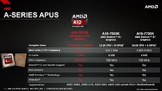
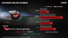
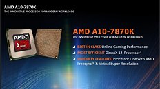
AMD today introduced the latest addition to its line of desktop A-Series processors, the A10-7870K APU, a refresh to the existing line of processors codenamed "Kaveri". The A10-7870K delivers a best-in-class experience for eSports and online gaming with superior performance, best-in-class efficiency in DirectX 12, and unique features. The new processor also delivers exceptional performance in modern workloads and is designed for the future with Microsoft Windows 10.

The latest iteration of the popular and powerful AMD A-Series APU family provides premium performance and multitasking powered by up to 12 compute cores (4 CPU + 8 GPU). The responsiveness and processing power of the A10-7870K APU enables an immersive user experience on Windows 10 PCs while offering an easy path for PC builders looking to upgrade to discrete-level graphics and faster processing at an afforadable price. The A10-7870K APU is available at e-tail now at a suggested price (SEP) of US $137, and through participating system builders.

AMD Radeon R9 380 Launched by PC OEM

Earlier this day, HP announced its newest line of desktop PCs, one of which comes with a curious-sounding Radeon R9 380 graphics card. HP's product pages for its new desktops aren't active, yet, leaving us to only speculate on what the R9 380 could be. One theory making rounds says that the R9 380 could either be a re-branded R9 285, or be based on its "Tonga" silicon, which physically features 2,048 stream processors based on Graphics CoreNext (GCN) 1.2 architecture, and a 384-bit wide GDDR5 memory interface. Another theory states that the R9 380 could be an OEM-only re-brand of the R9 280 or R9 280X, based on the 3+ year old "Tahiti" silicon.

The former theory sounds more plausible, because re-branding a "Tahiti" based product would be suicidal for AMD. Although based on GCN, "Tahiti" lacks a lot of architecture features introduced with "Hawaii" and "Tonga." AMD practically stopped optimizing games for "Tahiti," and some of its new features, such as FreeSync and XDMA CrossFire, can't be implemented on it. "Tonga," on the other hand, supports both these features, and one can create an SKU with all its 2,048 stream processors, and its full 384-bit GDDR5 memory interface unlocked. If the R9 380 is indeed an OEM-only product, then it's likely that the company's retail-channel products could be branded in the succeeding R9 400 series. GPU makers tend to re-brand and bump their SKUs by a series for OEMs to peddle in their "new" products at short notice.

AMD FirePro M5100 Powers Panasonic Toughbook CF-54

AMD today announced that Panasonic selected AMD FirePro M5100 mobile professional graphics to provide users on-the-move with quality, performance and innovation in a variety of work environments in the new Panasonic Toughbook CF-541. The Panasonic Toughbook CF-54 with AMD FirePro mobile professional graphics is designed to deliver outstanding graphics performance matched with world-class reliability for professionals in the automotive, telecommunications, construction, manufacturing, mining and defense industries or for professionals that require a portable workstation solution designed for a semi-harsh indoor or outdoor environment.

Panasonic Toughbook is legendary for its ruggedness and is widely known for its reliability and durability, even in extreme operating conditions. The inclusion of AMD FirePro mobile professional graphics creates a bold new category for architects, project managers and engineers who demand the ultimate combination of durability, reliability and workstation-class performance with certified application support.
Return to Keyword Browsing
Dec 18th, 2024 09:22 EST change timezone

New Forum Posts

Popular Reviews

Controversial News Posts