News Posts matching #HBM4

Return to Keyword Browsing

Samsung 6th-Gen DRAM Receives Production Readiness Approval

Samsung Electronics achieved a significant technological milestone by securing production readiness approval for its sixth-generation DRAM technology. Industry sources, as Korea Herald reports, confirmed on Tuesday that the company received internal authorization for mass production, marking completion of the advanced 10 nm-class process (called 1c DRAM) development. We recently reported that Samsung was able to achieve yield rates of 50-70% in testing for the 1c DRAM process as the company seems to be able to follow its projected timeline of approximately two years between product generations. The development holds particular significance for Samsung's high bandwidth memory (HBM) strategy since the company plans to commence HBM4 mass production during the second half of this year utilizing the newly developed sixth-generation DRAM technology. Samsung Electronics announced on May its adoption of hybrid bonding technology for future HBM4 memory stacks. The implementation aims to decrease thermal resistance while enabling ultra-wide memory interfaces, addressing the increasing bandwidth and efficiency requirements of artificial intelligence and high-performance computing applications.

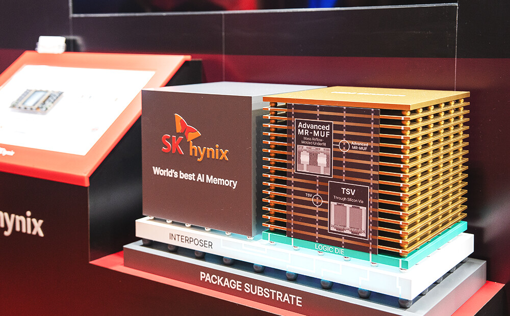
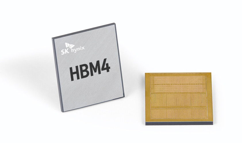
SK hynix, currently dominating the HBM market pursues HBM4 development using fifth-generation DRAM technology and started to deliver HBM4 samples to major clients in March, targeting similar production timelines for the latter half of this year. However, Samsung faces critical qualification requirements ahead as the company must deliver HBM4 samples and successfully complete NVIDIA's qualification testing to secure high-volume supply contracts. Additionally, Samsung continues awaiting qualification approval for its 12-layer HBM3E product while supplying AMD and looking for supply agreements with NVIDIA.

Intel "Jaguar Shores" Uses HBM4, "Diamond Rapids" Pairs with MRDIMM Gen 2 Memory

During the Intel AI Summit in Seoul, South Korea, Intel teased its upcoming product portfolio, featuring next-generation memory technologies. Being in Seoul, memory makers like SK Hynix are Intel's main partners for these products. Teased at the summit is Intel's upcoming AI accelerator, called "Jaguar Shores," which utilizes the next-generation HBM4 memory, offering 2.0 TB/s of bandwidth per module across 2,048 IO pins. SK Hynix plans to support this accelerator with its memory, ensuring that Intel's big data center-grade AI accelerator is equipped with the fastest memory on the market. Since the "Falcon Shores" accelerator is only intended for testing with external customers, we don't have an exact baseline to compare to, and Jaguar Shores specifications are scarce.

Next up, Intel confirmed that its upcoming seventh-generation "Diamond Rapids" Xeon processors will use the second generation of MRDIMMs (Multiplexer Rank Dual Inline Memory Modules), an upgrade from the first-generation MRDIMMs used in the Xeon 6 family. The upgrade to MRDIMMs Gen 2 will allow Intel to push transfer rates to 12,800 MT/s, up from 8,800 MT/s in Xeon 6 with MRDIMMs Gen 1. Alongside this 45% speed bump in raw transfer rates, the memory channels are jumping to 16, up from 12 in the current generation, yielding an additional bandwidth boost. Given that MRDIMMs operate by connecting more memory ranks using a multiplexer, and that these modules buffer data and commands, the increased data transfer rate comes without any additional signal degradation. As Intel is expected to pack more cores, this will be an essential piece in the toolbox to feed them and keep those cores busy on the Oak Stream platform, based on the LGA9324 socket.

Samsung Reportedly Achieves 70% Yields for Its 1c DRAM Technology

Samsung has achieved better production results for its advanced memory technology, according to Sedaily, as cited by TrendForce. The company's sixth-generation 10 nm DRAM, called 1c DRAM, now shows yield rates of 50-70% in testing. This represents a significant improvement from last year's results, which were below 30%. Samsung takes a different path from its rivals, while SK Hynix and Micron stick with 1b DRAM technology for HBM4 products, Samsung opts to create the newer 1c DRAM. This choice comes with more risk; however, it might bring bigger rewards, as the improved production rates enable Samsung to expand its manufacturing operations. The company plans to increase 1c DRAM production at its Hwaseong and Pyeongtaek facilities with expansion activities expected to begin before the end of this year.

These developments also support Samsung's HBM4 production schedule since the company aims to begin mass production of HBM4 products later this year. Yet, experts in the field point out that the product is still in its early stages and needs ongoing monitoring. Samsung planned to begin mass-producing sixth-gen 10 nm DRAM by late 2024. Instead, the company chose to remake the chip's design. This decision caused delays of more than one year however it was made to achieve better performance and yields. The new DRAM products will be manufactured at Samsung's Pyeongtaek Line 4 facility as these chips will serve both mobile and server applications. Separately, HBM4-related production will take place at Pyeongtaek Line 3.

Next‑Gen HBM4 to HBM8: Toward Multi‑Terabyte Memory on 15,000 W Accelerators

In a joint briefing this week, KAIST's Memory Systems Laboratory and TERA's Interconnection and Packaging group presented a forward-looking roadmap for High Bandwidth Memory (HBM) standards and the accelerator platforms that will employ them. Shared via Wccftech and VideoCardz, the outline covers five successive generations, from HBM4 to HBM8, each promising substantial gains in capacity, bandwidth, and packaging sophistication. First up is HBM4, targeted for a 2026 rollout in AI GPUs and data center accelerators. It will deliver approximately 2 TB/s per stack at an 8 Gbps pin rate over a 2,048-bit interface. Die stacks will reach 12 to 16 layers, yielding 36-48 GB per package with a 75 W power envelope. NVIDIA's upcoming Rubin series and AMD's Instinct MI500 cards are slated to employ HBM4, with Rubin Ultra doubling the number of memory stacks from eight to sixteen and AMD targeting up to 432 GB per device.

Looking to 2029, HBM5 maintains an 8 Gbps speed but doubles the I/O lanes to 4,096 bits, boosting throughput to 4 TB/s per stack. Power rises to 100 W and capacity scales to 80 GB using 16‑high stacks of 40 Gb dies. NVIDIA's tentative Feynman accelerator is expected to be the first HBM5 adopter, packing 400-500 GB of memory into a multi-die package and drawing more than 4,400 W of total power. By 2032, HBM6 will double pin speeds to 16 Gbps and increase bandwidth to 8 TB/s over 4,096 lanes. Stack heights can grow to 20 layers, supporting up to 120 GB per stack at 120 W. Immersion cooling and bumpless copper-copper bonding will become the norm. The roadmap then predicts HBM7 in 2035, which includes 24 Gbps speeds, 8,192-bit interfaces, 24 TB/s throughput, and up to 192 GB per stack at 160 W. NVIDIA is preparing a 15,360 W accelerator to accommodate this monstrous memory.

AMD Previews 432 GB HBM4 Instinct MI400 GPUs and Helios Rack‑Scale AI Solution

At its "Advancing AI 2025" event, AMD rolled out its new Instinct MI350 lineup on the CDNA 4 architecture and teased the upcoming UDNA-based AI accelerator. True to its roughly one‑year refresh rhythm, the company confirmed that the Instinct MI400 series will land in early 2026, showcasing a huge leap in memory, interconnect bandwidth, and raw compute power. Each MI400 card features twelve HBM4 stacks, providing a whopping 432 GB of on-package memory and pushing nearly 19.6 TB/s of memory bandwidth. Those early HBM4 modules deliver approximately 1.6 TB/s each, just shy of the 2 TB/s mark. On the compute front, AMD pegs the MI400 at 20 PetaFLOPS of FP8 throughput and 40 PetaFLOPS of FP4, doubling the sparse-matrix performance of today's MI355X cards. But the real game‑changer is how AMD is scaling those GPUs. Until now, you could connect up to eight cards via Infinity Fabric, and anything beyond that had to go over Ethernet.

The MI400's upgraded fabric link now offers 300 GB/s, nearly twice the speed of the MI350 series, allowing you to build full-rack clusters without relying on slower networks. That upgrade paves the way for "Helios," AMD's fully integrated AI rack solution. It combines upcoming EPYC "Venice" CPUs with MI400 GPUs and trim-to-fit networking gear, offering a turnkey setup for data center operators. AMD didn't shy away from comparisons, either. A Helios rack with 72 MI400 cards delivers approximately 3.1 ExaFLOPS of tensor performance and 31 TB of HBM4 memory. NVIDIA's Vera Rubin system, slated to feature 72 GPUs and 288 GB of memory each, is expected to achieve around 3.6 ExaFLOPS, with AMD's capabilities surpassing it in both bandwidth and capacity. And if that's not enough, whispers of a beefed‑up MI450X IF128 system are already swirling. Due in late 2026, it would directly link 128 GPUs with Infinity Fabric at 1.8 TB/s bidirectional per device, unlocking truly massive rack-scale AI clusters.

TSMC Prepares "CoPoS": Next-Gen 310 × 310 mm Packages

As demand for ever-growing AI compute power continues to rise and manufacturing advanced nodes becomes more difficult, packaging is undergoing its golden era of development. Today's advanced accelerators often rely on TSMC's CoWoS modules, which are built on wafer cuts measuring no more than 120 × 150 mm in size. In response to the need for more space, TSMC has unveiled plans for CoPoS, or "Chips on Panel on Substrate," which could expand substrate dimensions to 310 × 310 mm and beyond. By shifting from round wafers to rectangular panels, CoPoS offers more than five times the usable area. This extra surface makes it possible to integrate additional high-bandwidth memory stacks, multiple I/O chiplets and compute dies in a single package. It also brings panel-level packaging (PLP) to the fore. Unlike wafer-level packaging (WLP), PLP assembles components on large, rectangular panels, delivering higher throughput and lower cost per unit. Systems with PLP will be actually viable for production runs and allow faster iterations over WLP.

TSMC will establish a CoPoS pilot line in 2026 at its Visionchip subsidiary. In 2027, the pilot facility will focus on refining the process, to meet partner requirements by the end of the year. Mass production is projected to begin between the end of 2028 and early 2029 at TSMC's Chiayi AP7 campus. That site, chosen for its modern infrastructure and ample space, is also slated to host production of multi-chip modules and System-on-Wafer technologies. NVIDIA is expected to be the launch partner for CoPoS. The company plans to leverage the larger panel area to accommodate up to 12 HBM4 chips alongside several GPU chiplets, offering significant performance gains for AI workloads. At the same time, AMD and Broadcom will continue using TSMC's CoWoS-L and CoWoS-R variants for their high-end products. Beyond simply increasing size, CoPoS and PLP may work in tandem with other emerging advances, such as glass substrates and silicon photonics. If development proceeds as planned, the first CoPoS-enabled devices could reach the market by late 2029.

Micron Ships HBM4 Samples: 12-Hi 36 GB Modules with 2 TB/s Bandwidth

Micron has achieved a significant advancement of the HBM4 architecture, which will stack 12 DRAM dies (12-Hi) to provide 36 GB of capacity per package. According to company representatives, initial engineering samples are scheduled to ship to key partners in the coming weeks, paving the way for full production in early 2026. The HBM4 design relies on Micron's established 1β ("one-beta") process node for DRAM tiles, in production since 2022, while it prepares to introduce EUV-enabled 1γ ("one-gamma") later this year for DDR5. By increasing the interface width from 1,024 to 2,048 bits per stack, each HBM4 chip can achieve a sustained memory bandwidth of 2 TB/s, representing a 20% efficiency improvement over the existing HBM3E standard.

NVIDIA and AMD are expected to be early adopters of Micron's HBM4. NVIDIA plans to integrate these memory modules into its upcoming Rubin-Vera AI accelerators in the second half of 2026. AMD is anticipated to incorporate HBM4 into its next-generation Instinct MI400 series, with further information to be revealed at the company's Advancing AI 2025 conference. The increased capacity and bandwidth of HBM4 will address growing demands in generative AI, high-performance computing, and other data-intensive applications. Larger stack heights and expanded interface widths enable more efficient data movement, a critical factor in multi-chip configurations and memory-coherent interconnects. As Micron begins mass production of HBM4, major obstacles to overcome will be thermal performance and real-world benchmarks, which will determine how effectively this new memory standard can support the most demanding AI workloads.
Micron HBM4 Memory

Intel Details EMIB-T Advanced Packaging for HBM4 and UCIe

This week at the Electronic Components Technology Conference (ECTC), Intel introduced EMIB-T, an important upgrade to its embedded multi-die interconnect bridge packaging. First showcased at the Intel Foundry Direct Connect 2025 event, EMIB-T incorporates through-silicon vias (TSVs) and high-power metal-insulator-metal capacitors into the existing EMIB structure. According to Dr. Rahul Manepalli, Intel Fellow and vice president of Substrate Packaging Development, these changes allow a more reliable power supply and stronger communication between separate chiplets. Conventional EMIB designs have struggled with voltage drops because of their cantilevered power delivery paths. In contrast, EMIB-T routes power directly through TSVs from the package substrate to each chiplet connection. The integrated capacitors compensate for fast voltage fluctuations and preserve signal integrity.

This improvement will be critical for next-generation memory, such as HBM4 and HBM4e, where data rates of 32 Gb/s per pin or more are expected over a UCIe interface. Intel has confirmed that the first EMIB-T packages will match the current energy efficiency of around 0.25 picojoules per bit while offering higher interconnect density. The company plans to reduce the bump pitch below today's standard of 45 micrometers. Beginning in 2026, Intel intends to produce EMIB-based packages measuring 120 by 120 millimeters, roughly eight times the size of a single reticle. These large substrates could integrate up to twelve stacks of high-bandwidth memory alongside multiple compute chiplets, all connected by more than twenty EMIB bridges. Looking further ahead, Intel expects to push package dimensions to 120 by 180 millimeters by 2028. Such designs could accommodate more than 24 memory stacks, eight compute chiplets, and 38 or more EMIB bridges. These developments closely mirror similar plans announced by TSMC for its CoWoS technology. In addition to EMIB-T, Intel also presented a redesigned heat spreader that reduces voids in the thermal interface material by approximately 25%, as well as a new thermal-compression bonding process that minimizes warping in large package substrates.

SK hynix Presents Groundbreaking AI & Server Memory Solutions at DTW 2025

SK hynix presented its leading memory solutions optimized for AI servers and AI PCs at Dell Technologies World (DTW) 2025 in Las Vegas from May 19-22. Hosted by Dell Technologies, DTW is an annual conference which introduces future technology trends. In line with DTW 2025's theme of "Accelerate from Ideas to Innovation," a wide range of products and technologies aimed at driving AI innovation was showcased at the event.

Based on its close partnership with Dell, SK hynix has participated in the event every year to reinforce its leadership in AI. This year, the company organized its booth into six sections: HBM, CMM (CXL Memory Module)-DDR5, server DRAM, PC DRAM, eSSDs, and cSSDs. Featuring products with strong competitiveness across all areas of DRAM and NAND flash for the AI server, storage and PC markets, the booth garnered strong attention from visitors.

Samsung Prepares Hybrid Bonding for HBM4 to Slash Thermals and Boost Bandwidth

At the recent AI Semiconductor Forum in Seoul, Samsung Electronics revealed that it will adopt hybrid bonding in its upcoming HBM4 memory stacks. This decision is intended to reduce thermal resistance and enable an ultra‑wide memory interface, qualities that become ever more critical as artificial intelligence and high‑performance computing applications demand greater bandwidth and efficiency. Unlike current stacking methods that join DRAM dies with tiny solder microbumps and underfill materials, hybrid bonding bonds copper‑to‑copper and oxide‑to‑oxide surfaces directly, resulting in thinner, more thermally efficient 3D assemblies. High‑bandwidth memory works by stacking multiple DRAM dies on top of a base logic die, with through‑silicon vias carrying signals vertically through each layer. Traditionally, microbumps routed horizontal connections between dies, but as data rates increase and stack heights grow, these bumps introduce significant electrical and thermal limitations.

Hybrid bonding addresses those issues by allowing interconnect pitches below 10 micrometers, which lowers both resistance and capacitance and improves overall signal integrity. SK hynix has taken a different path. The company is enhancing its molded reflow underfill (MR‑MUF) process to produce 16‑Hi HBM4 stacks that comply with JEDEC's maximum height requirement of 775 micrometers. The company believes that if its advanced MR‑MUF technique can achieve performance on par with hybrid bonding, they will avoid the substantial capital investment needed for the specialized equipment that true 3D copper bonding requires. The cost and space demands of hybrid bonding equipment are significant. Specialized lithography and alignment tools occupy more clean‑room real estate, increasing capital expenditures. Samsung may mitigate some of these costs through Semes, its in‑house equipment subsidiary, but it remains uncertain whether Semes can deliver production‑ready hybrid bonding systems in time for mass production. If Samsung successfully qualifies its HBM4 stacks using hybrid bonding, which it plans to begin manufacturing in 2026, the company could gain a competitive edge over Micron and SK hynix.

Samsung Reportedly Courting HBM4 Supply Interest From Big Players

The vast majority of High Bandwidth Memory (HBM) new stories—so far, in 2025—have involved or alluded to new-generation SK hynix and Micron products. As mentioned in recently published Samsung Electronics Q1 financial papers, company engineers are still working on "upcoming enhanced HBM3E products." Late last month, a neighbor/main rival publicly showcased their groundbreaking HBM4 memory solution—indicating a market leading development position. Samsung has officially roadmapped a futuristic "sixth-generation" HBM4 technology, but their immediate focus seems to be a targeted sales expansion of incoming "enhanced HBM3E 12H" products. Previously, the firm's Memory Business has lost HBM3 ground—within AI GPU/accelerator market segments—to key competitors.

Industry insiders believe that company leadership will attempt to regain lost market shares in a post-2025 world. As reported by South Korean news outlets, Kim Jae-joon (VP of Samsung's memory department) stated—during a recent earnings call, with analysts—that his team is: "already collaborating with multiple customers on custom versions based on both HBM4 and the enhanced HBM4E." The initiation of commercial shipments is anticipated at some point in 2026, hinging on mass production starting by the second half of this year. The boss notified listeners about development "running on schedule." A Hankyung article alleges that Samsung HBM4 evaluation samples have been sent out to "NVIDIA, Broadcom, and Google." Wccftech posits a positive early outlook: "Samsung will use its own 4 nm process from the foundry division and utilize the 10 nm 6th-generation 1c DRAM, which is known as one of the highest-end in the market. On paper, (their) HBM4 solution will be on par with competing models (from SK hynix), but we will have to wait and see."

TSMC Outlines Roadmap for Wafer-Scale Packaging and Bigger AI Packages

At this year's Technology Symposium, TSMC unveiled an engaging multi-year roadmap for its packaging technologies. TSMC's strategy splits into two main categories: Advanced Packaging and System-on-Wafer. Back in 2016, CoWoS-S debuted with four HBM stacks paired to N16 compute dies on a 1.5× reticle-limited interposer, which was an impressive feat at the time. Fast forward to 2025, and CoWoS-S now routinely supports eight HBM chips alongside N5 and N4 compute tiles within a 3.3× reticle budget. Its successor, CoWoS-R, increases interconnect bandwidth and brings N3-node compatibility without changing that reticle constraint. Looking toward 2027, TSMC will launch CoWoS-L. First up are large N3-node chiplets, followed by N2-node tiles, multiple I/O dies, and up to a dozen HBM3E or HBM4 stacks—all housed within a 5.5× reticle ceiling. It's hard to believe that eight HBM stacks once sounded ambitious—now they're just the starting point for next-gen AI accelerators inspired by AMD's Instinct MI450X and NVIDIA's Vera Rubin.

Integrated Fan-Out, or InFO, adds another dimension with flexible 3D assemblies. The original InFO bridge is already powering AMD's Instinct cards. Later this year, InFO-POP (package-on-package) and InFO-2.5D arrive, promising even denser chip stacking and unlocking new scaling potential on a single package, away from the 2D and 2.5D packaging we were used to, going into the third dimension. On the wafer scale, TSMC's System-on-Wafer lineup—SoW-P and SoW-X—has grown from specialized AI engines into a comprehensive roadmap mirroring logic-node progress. This year marks the first SoIC stacks from N3 to N4, with each tile up to 830 mm² and no hard limit on top-die size. That trajectory points to massive, ultra-dense packages, which is exactly what HPC and AI data centers will demand in the coming years.

SK hynix Showcases HBM4 to Highlight AI Memory Leadership at TSMC 2025 Technology Symposium

SK hynix showcased groundbreaking memory solutions including HBM4 at the TSMC 2025 North America Technology Symposium held in Santa Clara, California on April 23. The TSMC North America Technology Symposium is an annual event in which TSMC shares its latest technologies and products with global partners. This year, SK hynix participated under the slogan "Memory, Powering AI and Tomorrow," highlighting its technological leadership in AI memory through exhibition zones including HBM Solutions and AI/Data Center Solutions.

In the HBM Solution section, SK hynix presented samples of its 12-layer HBM4 and 16-layer HBM3E products. The 12-layer HBM4 is a next-generation HBM capable of processing over 2 terabytes (TB) of data per second. In March, the company announced it has become the first in the world to supply HBM4 samples to major customers and plans to complete preparations for mass production within the second half of 2025. The B100, NVIDIA's latest Blackwell GPU equipped with the 8-layer HBM3E, was also exhibited in the section along with 3D models of key HBM technologies such as TSV and Advanced MR-MUF, drawing significant attention from visitors.

TSMC Unveils Next-Generation A14 Process at North America Technology Symposium

TSMC today unveiled its next cutting-edge logic process technology, A14, at the Company's North America Technology Symposium. Representing a significant advancement from TSMC's industry-leading N2 process, A14 is designed to drive AI transformation forward by delivering faster computing and greater power efficiency. It is also expected to enhance smartphones by improving their on-board AI capabilities, making them even smarter. Planned to enter production in 2028, the current A14 development is progressing smoothly with yield performance ahead of schedule.

Compared with the N2 process, which is about to enter volume production later this year, A14 will offer up to 15% speed improvement at the same power, or up to 30% power reduction at the same speed, along with more than 20% increase in logic density. Leveraging the Company's experience in design-technology co-optimization for nanosheet transistor, TSMC is also evolving its TSMC NanoFlex standard cell architecture to NanoFlex Pro, enabling greater performance, power efficiency and design flexibility.

JEDEC and Industry Leaders Collaborate to Release JESD270-4 HBM4 Standard

JEDEC Solid State Technology Association, the global leader in the development of standards for the microelectronics industry, today announced the publication of its highly anticipated High Bandwidth Memory (HBM) DRAM standard: HBM4. Designed as an evolutionary step beyond the previous HBM3 standard, JESD270-4 HBM4 will further enhance data processing rates while maintaining essential features such as higher bandwidth, power efficiency, and increased capacity per die and/or stack, because the higher bandwidth enables the higher data processing rate.

The advancements introduced by HBM4 are vital for applications that require efficient handling of large datasets and complex calculations, including generative artificial intelligence (AI), high-performance computing, high-end graphics cards, and servers. HBM4 introduces numerous improvements to the prior version of the standard, including:

GUC Announces Tape-Out of the World's First HBM4 IP on TSMC N3P

Global Unichip Corp. (GUC), the Advanced ASIC Leader, announced today that it has successfully taped-out the world's first HBM4 controller and PHY IP. This test chip was implemented using TSMC's cutting-edge N3P process technology and CoWoS -R advanced packaging technology.

The HBM4 IP supports data rates of up to 12 Gbps under all operating conditions. By leveraging a proprietary interposer layout, GUC has optimized signal integrity (SI) and power integrity (PI) to achieve these high speeds for all types of CoWoS technology. Comparing with HBM3, GUC's HBM4 PHY delivers 2.5x bandwidth while improving 1.5x power efficiency and 2x area efficiency. In line with previous GUC HBM, GLink, and UCIe IPs, this HBM4 IP integrates proteanTecs' interconnect monitoring solution to provide high visibility for testing and characterizing the PHY while improving in-field performance and reliability for end products.

Micron Announces Memory Price Increases for 2025-2026 Amid Supply Constraints

In a letter to customers, Micron has announced upcoming memory price increases extending through 2025 and 2026, citing persistent supply constraints coupled with accelerating demand across its product portfolio. The manufacturer points to significant demand growth in DRAM, NAND flash, and high-bandwidth memory (HBM) segments as key drivers behind the pricing strategy. The memory market is rebounding from a prolonged oversupply cycle that previously depressed revenues industry-wide. Strategic production capacity reductions implemented by major suppliers have contributed to price stabilization and subsequent increases over the past twelve months. This pricing trajectory is expected to continue as data center operators, AI deployments, and consumer electronics manufacturers compete for limited memory allocation.

In communications to channel partners, Micron emphasized AI and HPC requirements as critical factors necessitating the price adjustments. The company has requested detailed forecast submissions from partners to optimize production planning and supply chain stability during the constrained market period. With its pricing announcement, Micron disclosed a $7 billion investment in a Singapore-based HBM assembly facility. The plant will begin operations in 2026 and will focus on HBM3E, HBM4, and HBM4E production—advanced memory technologies essential for next-generation AI accelerators and high-performance computing applications from NVIDIA, AMD, Intel, and other companies. The price increases could have cascading effects across the AI and GPU sector, potentially raising costs for products ranging from consumer gaming systems to enterprise data infrastructure. We are monitoring how these adjustments will impact hardware refresh cycles and technology adoption rates as manufacturers pass incremental costs to end customers.

SK hynix Ships World's First 12-Layer HBM4 Samples to Customers

SK hynix Inc. announced today that it has shipped the samples of 12-layer HBM4, a new ultra-high performance DRAM for AI, to major customers for the first time in the world. The samples were delivered ahead of schedule based on SK hynix's technological edge and production experience that have led the HBM market, and the company is to start the certification process for the customers. SK hynix aims to complete preparations for mass production of 12-layer HBM4 products within the second half of the year, strengthening its position in the next-generation AI memory market.

The 12-layer HBM4 provided as samples this time feature the industry's best capacity and speed which are essential for AI memory products. The product has implemented bandwidth capable of processing more than 2 TB (terabytes) of data per second for the first time. This translates to processing data equivalent to more than 400 full-HD movies (5 GB each) in a second, which is more than 60 percent faster than the previous generation, HBM3E.

NVIDIA Confirms: "Blackwell Ultra" Coming This Year, "Vera Rubin" in 2026

During its latest FY2024 earnings call, NVIDIA's CEO Jensen Huang gave a few predictions about future products. The upcoming Blackwell B300 series, codenamed "Blackwell Ultra," is scheduled for release in the second half of 2025. It will feature significant performance enhancements over the B200 series. These GPUs will incorporate eight stacks of 12-Hi HBM3E memory, providing up to 288 GB of onboard memory, paired with the Mellanox Spectrum Ultra X800 Ethernet switch, which offers 512 ports. Earlier rumors suggested that this is a 1,400 W TBP chip, meaing that NVIDIA is packing a lot of compute in there. There is a potential 50% performance increase compared to current-generation products. However, NVIDIA has not officially confirmed these figures, but rough estimates of core count and memory bandwidth increase can make it happen.

Looking beyond Blackwell, NVIDIA is preparing to unveil its next-generation "Rubin" architecture, which promises to deliver what Huang described as a "big, big, huge step up" in AI compute capabilities. The Rubin platform, targeted for 2026, will integrate eight stacks of HBM4(E) memory, "Vera" CPUs, NVLink 6 switches delivering 3600 GB/s bandwidth, CX9 network cards supporting 1600 Gb/s, and X1600 switches—creating a comprehensive ecosystem for advanced AI workloads. More surprisingly, Huang indicated that NVIDIA will discuss post-Rubin developments at the upcoming GPU Technology Conference in March. This could include details on Rubin Ultra, projected for 2027, which may incorporate 12 stacks of HBM4E using 5.5-reticle-size CoWoS interposers and 100 mm × 100 mm TSMC substrates, representing another significant architectural leap forward in the company's accelerating AI infrastructure roadmap. While these may seem distant, NVIDIA is battling supply chain constraints to deliver these GPUs to its customers due to the massive demand for its solutions.

SK hynix Announces 4Q24 Financial Results

SK hynix Inc. announced today that it recorded best-ever yearly performance with 66.1930 trillion won in revenues, 23.4673 trillion won in operating profit (with an operating margin of 35%), and 19.7969 trillion won in net profit (with a net margin of 30%). Yearly revenues marked all-time high, exceeding the previous record in 2022 by over 21 trillion won and operating profit exceeded the record in 2018 during the semiconductor super boom.

In particular, fourth quarter revenues went up by 12% to 19.7670 trillion won, operating profit up 15% to 8.0828 trillion won (with an operating margin of 41%) from the previous quarter and net profit recorded 8.0065 trillion won (with a net margin of 41%). SK hynix emphasized that with prolonged strong demand for AI memory, the company achieved all-time high result through world-leading HBM technology and profitability-oriented operation. HBM continued its high growth in fourth quarter marking over 40% of total DRAM revenue and eSSD also showed constant increase in sales. With remarkable product competitiveness based profitability-oriented operation, the company established a stable financial condition which led to improved outcome.

SK hynix Ships HBM4 Samples to NVIDIA in June, Mass Production Slated for Q3 2025

SK hynix has sped up its HBM4 development plans, according to a report from ZDNet. The company wants to start shipping HBM4 samples to NVIDIA this June, which is earlier than the original timeline. SK hynix hopes to start supplying products by the end of Q3 2025, this push likely aims to get a head start in the next-gen HBM market. To meet this sped-up schedule, SK hynix has set up a special HBM4 development team to supply NVIDIA. Industry sources indicated on January 15th that SK Hynix plans to deliver its first customer samples of HBM4 in early June this year. The company hit a big milestone when it wrapped up the HBM4 tapeout in Q4 2024, the last design step.

HBM4 marks the sixth iteration of high-bandwidth memory tech using stacked DRAM architecture. It comes after HBM3E, the current fifth-gen version, with large-scale production likely to kick off in late 2025 at the earliest. HBM4 boasts a big leap forward doubling data transfer ability with 2,048 I/O channels up from its forerunner. NVIDIA planned to use 12-layer stacked HBM4 in its 2026 "Rubin" line of powerful GPUs. However, NVIDIA has moved up its timeline for "Rubin" aiming to launch in late 2025.

NVIDIA's Next-Gen "Rubin" AI GPU Development 6 Months Ahead of Schedule: Report

The "Rubin" architecture succeeds NVIDIA's current "Blackwell," which powers the company's AI GPUs, as well as the upcoming GeForce RTX 50-series gaming GPUs. NVIDIA will likely not build gaming GPUs with "Rubin," just like it didn't with "Hopper," and for the most part, "Volta." NVIDIA's AI GPU product roadmap put out at SC'24 puts "Blackwell" firmly in charge of the company's AI GPU product stack throughout 2025, with "Rubin" only succeeding it in the following year, for a two-year run in the market, being capped off with a "Rubin Ultra" larger GPU slated for 2027. A new report by United Daily News (UDN), a Taiwan-based publication, says that the development of "Rubin" is running 6 months ahead of schedule.

Being 6 months ahead of schedule doesn't necessarily mean that the product will launch sooner. It would give NVIDIA headroom to get "Rubin" better evaluated in the industry, and make last-minute changes to the product if needed; or even advance the launch if it wants to. The first AI GPU powered by "Rubin" will feature 8-high HBM4 memory stacks. The company will also introduce the "Vera" CPU, the long-awaited successor to "Grace." It will also introduce the X1600 InfiniBand/Ethernet network processor. According to the SC'24 roadmap by NVIDIA, these three would've seen a 2026 launch. Then in 2027, the company would follow up with an even larger AI GPU based on the same "Rubin" architecture, codenamed "Rubin Ultra." This features 12-high HBM4 stacks. NVIDIA's current GB200 "Blackwell" is a tile-based GPU, with two dies that have full cache-coherence. "Rubin" is rumored to feature four tiles.

SK Hynix Shifts to 3nm Process for Its HBM4 Base Die in 2025

SK Hynix plans to produce its 6th generation high-bandwidth memory chips (HBM4) using TSMC's 3 nm process, a change from initial plans to use the 5 nm technology. The Korea Economic Daily reports that these chips will be delivered to NVIDIA in the second half of 2025. NVIDIA's GPU products are currently based on 4 nm HBM chips. The HBM4 prototype chip launched in March by SK Hynix features vertical stacking on a 3 nm die., compared to a 5 nm base die, the new 3 nm-based HBM chip is expected to offer a 20-30% performance improvement. However, SK Hynix's general-purpose HBM4 and HBM4E chips will continue to use the 12 nm process in collaboration with TSMC.

While SK Hynix's fifth-generation HBM3E chips used its own base die technology, the company has chosen TSMC's 3 nm technology for HBM4. This decision is anticipated to significantly widen the performance gap with competitor Samsung Electronics, which plans to manufacture its HBM4 chips using the 4 nm process. SK hynix is currently leading the global HBM market with almost 50% of market share, most of its HBM products been delivered to NVIDIA.

NVIDIA CEO Jensen Huang Asks SK hynix to Speed Up HBM4 Delivery by Six Months

SK hynix announced the first 48 GB 16-high HBM3E in the industry at the SK AI Summit in Seoul today. During the event, news came out about newer plans to develop their next-gen memory tech. Reuters and ZDNet Korea reported that NVIDIA CEO Jensen Huang asked SK hynix to speed up their HBM4 delivery by six months. SK Group Chairman Chey Tae-won shared this info at the Summit. The company had earlier said they would give HBM4 chips to customers in the second half of 2025.

When ZDNet asked about this sped-up plan, SK hynix President Kwak Noh-Jung gave a careful answer saying "We will give it a try." A company spokesperson told Reuters that this new schedule would be quicker than first planned, but they didn't share more details. In a video interview shown at the Summit, NVIDIA's Jensen Huang pointed out the strong team-up between the companies. He said working with SK hynix has helped NVIDIA go beyond Moore's Law performance gains. He stressed that NVIDIA will keep needing SK hynix's HBM tech for future products. SK hynix plans to supply the latest 12-layer HBM3E to an undisclosed customer this year, and will start sampling of the 16-layer HBM3E early next year.

HBM5 20hi Stack to Adopt Hybrid Bonding Technology, Potentially Transforming Business Models

TrendForce reports that the focus on HBM products in the DRAM industry is increasingly turning attention toward advanced packaging technologies like hybrid bonding. Major HBM manufacturers are considering whether to adopt hybrid bonding for HBM4 16hi stack products but have confirmed plans to implement this technology in the HBM5 20hi stack generation.

Hybrid bonding offers several advantages when compared to the more widely used micro-bumping. Since it does not require bumps, it allows for more stacked layers and can accommodate thicker chips that help address warpage. Hybrid-bonded chips also benefit from faster data transmission and improved heat dissipation.
Return to Keyword Browsing
Jul 5th, 2025 16:20 CDT change timezone

New Forum Posts

Popular Reviews

TPU on YouTube

Controversial News Posts