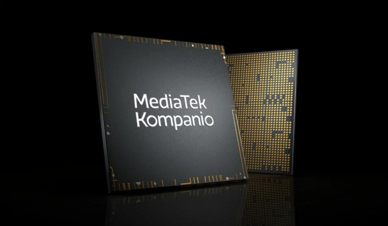
News Posts matching #LPDDR4X

Return to Keyword Browsing

Apple's A12Z SoC Features the Same A12X Silicon

With an introduction of new iPad Pro tablets, Apple has brought another new silicon to its offerings in the form of A12Z SoC. Following the previous king in tablet space, the A12X SoC, Apple has decided to update its silicon and now there is another, more advanced stepping in form of an A12Z SoC. Thanks to the report from TechInsights, their analysis has shown that the new SoC used in Apple's devices is pretty much the same compared to the A12X SoC of last year, except the GPU used. Namely, the configuration of A12X is translated into the A12Z - there are four Apple Vortex and four Apple Tempest cores for the CPU. There is a 128-bit memory bus designed for LPDDR4X memory, the same as the A12X.

What is different, however, is the GPU cluster configuration. In A12X there was a cluster filled with 7 working and one disabled A12-gen GPU core. In A12Z SoC all of the 8 GPUs present are enabled and working, and they are also of the same A12 generation. The new SoC is even built using the same N7 7 nm manufacturing process from TSMC. While we don't know the silicon stepping revision of the A12Z, there aren't any new features besides the additional GPU core.
Apple A12Z Bionic

Intel Core i5-L16G7 is the first "Lakefield" SKU Appearance, Possible Prelude to New Nomenclature?

Intel Core i5-L16G7 is the first commercial SKU that implements Intel's "Lakefield" heterogenous x86 processor architecture. This 5-core chip features one high-performance "Sunny Cove" CPU core, and four smaller "Tremont" low-power cores, with an intelligent scheduler balancing workloads between the two core types. This is essentially similar to ARM big.LITTLE. The idea being that the device idles most of the time, when lower-powered CPU cores can hold the fort; performance cores kick in only when really needed, until which time they remain power-gated. Thai PC enthusiast TUM_APISAK discovered the first public appearance of the i5-L16G7 in an unreleased Samsung device that has the Userbenchmark device ID string "SAMSUNG_NP_767XCL."

Clock speeds of the processor are listed as "1.40 GHz base, with 1.75 GHz turbo," but it's possible that the two core types have different clock-speed bands, just like the cores on big.LITTLE SoCs. Other key components of "Lakefield" include an iGPU based on the Gen11 graphics architecture, and an LPDDR4X memory controller. "Lakefield" implements Foveros packaging, in which high-density component dies based on newer silicon fabrication nodes are integrated with silicon interposers based on older fabrication processes, which facilitate microscopic high-density wiring between the dies. In case of "Lakefield," the Foveros package features a 10 nm "compute field" die sitting atop a 22 nm "base field" interposer.

A Walk Through SK Hynix at CES 2020: 4D NAND SSDs and DDR5 RDIMMs

Korean DRAM and NAND flash giant SK Hynix brought its latest memory innovations to the 2020 International CES. The star attraction at their booth was the "4D NAND" technology, and some of the first client-segment SSDs based on it. As a concept, 4D NAND surfaced way back in August 2018, and no, it doesn't involve the 4th dimension. Traditional 3D NAND chips use charge-trap flash (CTF) stacks spatially located next to a peripheral block that's responsible for wiring out all of those CTF stacks. In 4D NAND, the peripheral block is stacked along with the CTF stack itself, conserving real-estate on the 2-D plane (which can then be spent on increasing density). We caught two 128-layer 4D NAND-based client-segment drives inbound for 2020, the Platinum P31 M.2 NVMe, and Gold P31 M.2 NVMe. The already launched Gold S31 SATA drive was also there.

SK hynix Displays its Semiconductor Technologies Leading the 4th Industrial Revolution

SK hynix Inc. presents its innovative semiconductor technologies leading the 4th Industrial Revolution at CES 2020, the world's largest trade show for IT and consumer electronics in Las Vegas, USA, from January 7-10, 2020. In line with its "Memory Centric World" theme, SK hynix depicts a futuristic city which effectively utilizes enormous amounts of data. The Company also showcases its semiconductor solutions across six crucial business fields - artificial intelligence (AI), augmented reality (AR) / virtual reality (VR), automotive, Internet of Things (IoT), big data and 5G.

Headlining at CES 2020 are SK hynix's memory solutions including HBM2E, DDR5 for servers, and SSD, which are already highly regarded and widely used in 4th industrial fields such as 5G and AI for their stability, speed, power consumption and density excellence. Other cutting-edge products set to make headlines in January are the Company's highly durable LPDDR4X and eMMC 5.1, which are optimized for automobiles. What's more, SK hynix is displaying its LPDDR5 and UFS that enhance the performance of 5G smartphones as well as CIS (CMOS Image Sensor) which is essential in establishing effective environments for AR/VR and IoT.

AMD Announces Ryzen 4000 Mobile Processors: 4800U and 4800H

AMD today announced its Ryzen 4000-series mobile processors designed to compete with Intel's fastest, across both its 10th gen "Ice Lake" and "Comet Lake" mobile processors lines. At the heart of these processors is the 7 nm "Renoir" silicon, which doubles the CPU core count over the previous generation "Picasso," and improves IPC (single-thread performance) by a double-digit percentage. "Renoir" combines a CPU with 8 cores based on the "Zen 2" microarchitecture, with an iGPU that has the number-crunching machinery of "Vega," but with display- and multimedia-engines of "Navi." It is a monolithic piece of silicon with a dual-channel IMC that supports not just conventional DDR4 memory, but also fast LPDDR4X.

There are two distinct classes of Ryzen 4000 Mobile: U and H. The Ryzen 7 4800U, with its 15 W TDP, targets ultra-portable notebooks, and goes head-on against Intel's Core i7 "Ice Lake-U" processors, winning on the CPU front with its high core-count and IPC. The Ryzen 7 4800H, on the other hand, taps into the 45 W TDP headroom to dial up CPU and iGPU clock-speeds significantly, offering CPU performance that beats the desktop Core i7-9700K. It also introduces SmartShift, an iGPU + dGPU virtualization technology that lets your notebook dynamically switch between the two based on graphics load.

MSI Teases Evoke Line of Notebooks for Creators

MSI debuted the Evoke brand of hardware targeted at creators, with its Radeon RX 5700-series Evoke graphics cards. The company is now planning to extend the brand to a range of other products, beginning with notebooks. The company teased the design of what's allegedly the first Evoke branded notebook, which ships with a minimalist and durable design, and hardware tailored for content-creation applications. The company didn't tease its specs, but you can expect anything from Intel's 10th gen "Comet Lake-H" to AMD's Ryzen 4000 "Renoir" processors, and discrete graphics options that include RX 5500M "Navi" or even Max-Q RTX 20-series. Some of the higher trims could even leverage fast NVMe storage. MSI is expected to launch its Evolve notebooks on 7th January, 2020.

Intel "Tiger Lake-U" Processors Could Support LPDDR5 Memory

Intel's Core "Tiger Lake" microarchitecture could be a point of transition between DDR4 and DDR5 for the company. Prototypes of devices based on the ultra-compact "Tiger Lake-Y" SoC were earlier shown featuring LPDDR4X memory, although a new device, possibly a prototyping platform, in the regulatory queue with the Eurasian Economic Commission describes itself as featuring a "Tiger Lake-U" chip meant for thin and light notebooks and convertibles. This device features newer LPDDR5 memory, according to its regulatory filing.

LPDDR5 succeeds LPDDR4X as the industry's next low-power memory standard, offering data-rates of up to 6,400 MT/s (versus up to 4,266 MT/s of LPDDR4X), and consumes up to 30 percent less power. This prototype at the EEC is sure to be using unreleased LPDDR5 memory chips as DRAM majors Samsung and SK Hynix plan to ship their DDR5-based memory solutions only by the end of this year, although mass-production of the chips have already started at Samsung, in PoP form-factors. A successor to the 10th generation Core "Ice Lake," "Tiger Lake" will be Intel's second CPU microarchitecture designed for its 10 nm silicon fabrication node.

Samsung Begins Mass-production of 12GB LPDDR4X uMCP Memory Chips

Samsung Electronics, a world leader in advanced memory technology, today announced that it has begun mass producing the industry's first 12-gigabyte (GB) low-power double data rate 4X (LPDDR4X) UFS-based multichip package (uMCP). The announcement was made as part of the company's annual Samsung Tech Day at its Device Solutions' America headquarters in San Jose, California.

"Leveraging our leading-edge 24-gigabit (Gb) LPDDR4X chips, we can offer the highest mobile DRAM capacity of 12 GB not only for high-end smartphones but also for mid-range devices," said Sewon Chun, executive vice president of Memory Marketing at Samsung Electronics. "Samsung will continue to support our smartphone-manufacturing customers with on-time development of next-generation mobile memory solutions, bringing enhanced smartphone experiences to many more users around the globe."

AMD "Renoir" APU to Support LPDDR4X Memory and New Display Engine

AMD's next-generation "Renoir" APU, which succeeds the company's 12 nm "Picasso," will be the company's truly next-generation chip to feature an integrated graphics solution. It's unclear as of now, if the chip will be based on a monolithic die, or if it will be a multi-chip module of a 7 nm "Zen 2" chiplet paired with an enlarged I/O controller die that has the iGPU. We're getting confirmation on two key specs - one, that the iGPU will be based on the older "Vega" graphics architecture, albeit with an updated display engine to support the latest display standards; and two, that the processor's memory controller will support the latest LPDDR4X memory standard, at speeds of up to 4266 MHz DDR. In comparison, Intel's "Ice Lake-U" chip supports LPDDX4X up to 3733 MHz.

Code-lines pointing toward "Vega" graphics with an updated display controller mention the new DCN 2.1, found in AMD's new "Navi 10" GPU. This controller supports resolutions of up to 8K, DSC 1.2a, and new resolutions of 4K up to 240 Hz and 8K 60 Hz over a single cable, along with 30 bits per pixel color. The multimedia engine is also suitably updated to VCN 2.1 standard, and provides hardware-accelerated decoding for some of the newer video formats, such as VP9 and H.265 at up to 90 fps at 4K, and 8K up to 24 fps, and H.264 up to 150 fps at 4K. There's no word on when "Renoir" comes out, but a 2020 International CES unveil is likely.

Samsung Launches Highest-capacity Mobile DRAM

Samsung Electronics Co., Ltd., the world leader in advanced memory technology, today announced that it has begun mass producing the highest-capacity mobile DRAM - the industry's first 12-gigabyte (GB) low-power double data rate 4X (LPDDR4X) package - optimized for tomorrow's premium smartphones. Featuring higher capacity than most ultra-thin notebooks, the new mobile DRAM will enable smartphone users to take full advantage of all the features in next-generation smartphones.

"With mass production of the new LPDDR4X, Samsung is now providing a comprehensive lineup of advanced memory to power the new era of smartphones, from 12GB mobile DRAM to 512GB eUFS 3.0 storage," said Sewon Chun, executive vice president of Memory Marketing at Samsung Electronics. "Moreover, with the LPDDR4X, we're strengthening our position as the premium mobile memory maker best positioned to accommodate rapidly growing demand from global smartphone manufacturers."

Samsung Begins Mass Producing 2nd-Gen 10nm-Class, 16Gb LPDDR4X Mobile DRAM

Samsung Electronics, the world leader in advanced memory technology, today announced that it has begun mass producing the industry's first 2nd-generation of 10-nanometer-class (1y-nm), LPDDR4X (Low Power, Double Data Rate, 4X) DRAM to improve the efficiency and lower the battery drain of today's premium smartphones and other mobile applications. Compared to the mobile DRAM memory chips most used in current flagship mobile devices (1x-nm 16Gb LPDDR4X), the 2nd- generation LPDDR4X DRAM features up to a 10 percent power reduction while maintaining the same data rate of 4,266 megabits per second (Mb/s).

"The advent of 10nm-class mobile DRAM will enable significantly enhanced solutions for next-generation, flagship mobile devices that should first hit the market late this year or the first part of 2019." said Sewon Chun, senior vice president of Memory Sales & Marketing at Samsung Electronics. "We will continue to grow our premium DRAM lineup to lead the 'high-performance, high capacity, and low power' memory segment to meet the market demand and strengthen our business competitiveness."
Return to Keyword Browsing
Sep 17th, 2024 04:37 EDT change timezone

New Forum Posts

Popular Reviews

Controversial News Posts