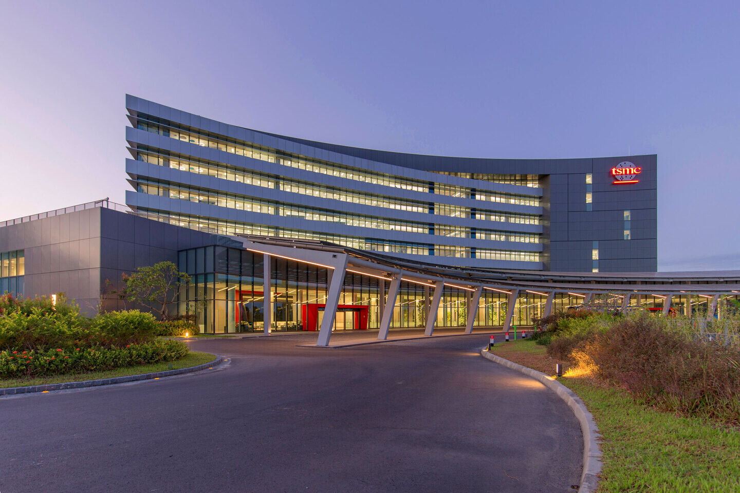
Apr 10th, 2025 13:23 EDT change timezone

New Forum Posts

Popular Reviews

Controversial News Posts

News Posts matching #N3

Return to Keyword Browsing

AMD's CEO Lisa Su Planning Trip to Taiwan, Said to be Visiting TSMC to Secure Future Wafer Allocation

Based on a report by Tom's Hardware, AMD's CEO Lisa Su is planning a trip to Taiwan in the next couple of months. It is said that she is planning to meet with multiple partners in Taiwan, such as ASUS, Acer and maybe more importantly, ASMedia, which will be the sole maker of chipsets for AMD, once the X570 chipset is discontinued. AMD is apparently also seeing various less well known partners that deliver parts for its CPUs, such as Nan Ya PCB, Unimicron Technologies and Kinsus Interconnects.

However, it appears that the main reason for Lisa Su herself to visit Taiwan will be to meet with TSMC, to discuss future collaboration with CC Wei, TSMC's chief executive. This is so AMD can secure enough wafer allocation on future nodes, such as its 3 nm and 2 nm class nodes. The move to these nodes is obviously not happening in the near future for AMD, but considering that TSMC is currently the leading foundry and is operating at capacity, it makes sense to get in early, as the competition is stiff when it comes to getting wafer allocation on cutting edge nodes. It's unclear which exact 3 nm class node AMD will be aiming for, but it might be the N3P node, which is said to kick off production sometime next year. Lisa Su is also said to have meetings with TSMC, SPIL and Ase Technology when it comes to advanced packaging for AMD's products. This includes technologies such as chip-on-wafer-on-substrate (CoWoS) and fan-out embedded bridge (FO-EB), with AMD already being expected to use some of these technologies in its upcoming Navi 3x GPUs.

TSMC has Seven Major Customers Lined Up for its 3 nm Node

Based on media reports out of Taiwan, TSMC seems to have plenty of customers lined up for its 3 nm node, with Apple being the first customer out the gates when production starts sometime next month. However, TSMC is only expected to start the production with a mere 1,000 wafer starts a month, which seems like a very low figure, especially as this is said to remain unchanged through all of Q4. On the plus side, yields are expected to be better than the initial 5 nm node yields. Full-on mass production for the 3 nm node isn't expected to happen until the second half of 2023 and TSMC will also kick off its N3E node sometime in 2023.

Apart from Apple, major customers for the 3 nm node include AMD, Broadcom, Intel, MediaTek, NVIDIA and Qualcomm. Contrary to earlier reports by TrendForce, it appears that TSMC will continue its rollout of the 3 nm node as previously planned. Apple is expected to produce the A17 smartphone and tablet SoC, as well as advanced versions of the M2, as well as the M3 laptop and desktop processors on the 3 nm node. Intel is still said to be producing its graphics chiplets with TSMC, with the potential for GPU and FPGA products in the future. There's no word on what the other customers are planning to produce on the 3 nm node, but MediaTek and Qualcomm are obviously looking at using the node for future smartphone and tablet SoCs, with AMD and NVIDIA most likely aiming for upcoming GPUs and Broadcom for some kind of HPC related hardware.

TSMC Announces the N3 FinFlex, N3E, and N2 Nodes, and 3DFabric

TSMC today showcased the newest innovations in its advanced logic, specialty, and 3D IC technologies at the Company's 2022 North America Technology Symposium, with the next-generation leading-edge N2 process powered by nanosheet transistors and the unique FINFLEX technology for the N3 and N3E processes making their debut.

Resuming as an in-person event after being held online in the past two years, the North America symposium in Santa Clara, California, kicks off a series of Technology Symposiums around the world in the coming months. The Symposiums also feature an Innovation Zone that spotlights the achievements of TSMC's emerging start-up customers.

Cadence Digital and Custom/Analog Design Flows Certified by TSMC for Latest N3E and N4P Processes

Cadence Design Systems, Inc. today announced that its digital and custom/analog design flows have been certified for the TSMC N3E and N4P processes, supporting the latest Design Rule Manual (DRM). In addition, Cadence and TSMC delivered N3E and N4P process design kits (PDKs) and design flows to accelerate customer adoption and advance mobile, AI and hyperscale computing design innovation. Joint customers are actively designing with the new N3E and N4P PDKs, and several test chips have already been taped out, which demonstrates how Cadence solutions help customers improve engineering efficiency and maximize the power, performance and area (PPA) benefits offered by the latest TSMC process technologies. The Cadence digital and custom/analog advanced-node solutions support the company's Intelligent System Design strategy, enabling system-on-chip (SoC) design excellence.

Cadence worked closely with TSMC to ensure the digital full flow was optimized for TSMC's advanced N3E and N4P process technologies. The complete RTL-to-GDS flow includes the Cadence Innovus Implementation System, Quantus Extraction Solution, Quantus Field Solver, Tempus Timing Signoff Solution and ECO option, Pegasus Verification System, Liberate Characterization Solution and Voltus IC Power Integrity Solution. Additionally, the Cadence Genus Synthesis Solution and predictive iSpatial technology are enabled for the TSMC N3E and N4P process technologies.

Intel "Meteor Lake" 2P+8E Silicon Annotated

Le Comptoir du Hardware scored a die-shot of a 2P+8E core variant of the "Meteor Lake" compute tile, and Locuza annotated it. "Meteor Lake" will be Intel's first processor to implement the company's IDM 2.0 strategy to the fullest. The processor is a multi-chip module of various tiles (chiplets), each with a certain function, sitting on die made on a silicon fabrication node most suitable to that function. Under this strategy, for example, if Intel's chip-designers calculate that the iGPU will be the most power-hungry component on the processor, followed by the CPU cores, the graphics tile will be built on a more advanced process than the compute tile. Intel's "Meteor Lake" and "Arrow Lake" processors will implement chiplets built on the Intel 4, TSMC N3, and Intel 20A fabrication nodes, each with unique power and transistor-density characteristics. Learn more about the "Meteor Lake" MCM in our older article.

The 2P+8E (2 performance cores + 8 efficiency cores) compute tile is one among many variants of compute tiles Intel will develop for the various SKUs making up the next-generation Core mobile processor series. The die is annotated with the two large "Redwood Cove" P-cores and their cache slices taking up about 35% of the die area; and the two "Crestmount" E-core clusters (each with 4 E-cores), and their cache slices, taking up the rest. The two P-cores and two E-core clusters are interconnected by a Ring Bus, and share an L3 cache. The size of each L3 cache slice is either 2.5 MB or 3 MB. At 2.5 MB, the total L3 cache will be 10 MB, and at 3 MB, it will be 12 MB. As with all past generations, the L3 cache is fully accessible by all CPU cores in the compute tile.

TSMC First Quarter 2022 Financials Show 45.1% Increase in Revenues

A new quarter and another forecast shattering revenue report from TSMC, as the company beat analysts' forecasts by over US$658 million, with a total revenue for the quarter of US$17.6 billion and a net income of almost US$7.26 billion. That's an increase in net income of 45.1 percent or 35.5 percent in sales. Although the monetary figures might be interesting to some, far more interesting details were also shared, such as production updates about future nodes. As a followup on yesterday's news post about 3 nanometer nodes, the N3 node is officially on track for mass production in the second half of this year. TSMC says that customer engagement is stronger than at the start of its N7 and N7 nodes, with HPC and smartphone chip makers lining up to get onboard. The N3E node is, as reported yesterday, expected to enter mass production in the second half of 2023, or a year after N3. Finally, the N2 node is expected in 2025 and won't adhere to TSMC's two year process technology cadence.

Breaking down the revenue by nodes, N7 has taken back the lead over N5, as N7 accounted for 30 percent of TSMC's Q1 revenues up from 27 percent last quarter, but down from 35 percent in the previous year. N5 sits at 20 percent, which is down from 23 percent in the previous quarter, but up from 14 percent a year ago. The 16 and 28 nm nodes still hold on to 25 percent of TSMC's revenue, which is the same as a year ago and up slightly from the previous quarter. Remaining nodes are unchanged from last quarter.

TSMC's N3E Node Said to Have Good Yields, Volume Production Expected Q2 2023

Back in March there were reports of TSMC's N3E node having been moved from 2024 to the end of 2023. However, it seems like the node is already seeing better than expected yields and is now being pulled in further and TSMC is expecting to start volume production as early as Q2 in 2023. The node does appear to have been frozen when it comes to further development as of the end of March. Yields are said to be much higher than the N3B node, which is also under development, but with limited information available about it.

The first customer for the new node is expected to be Apple, as the company is largely paying for much of the cutting edge node development at TSMC. However, both Intel and Qualcomm are said to be some of the first customers for the new node. More details should hopefully be announced tomorrow during TSMC's first quarter earnings call. The N3E node is a reduced layer EUV process, but before it goes into mass production, it's likely we'll be seeing the N3 node first. Early production of 3 nm parts later this year is expected to be at around 10 to 20k wafers per month initially, rising to about 25 to 35k a month once TSMC's new fab is ready. Once the N3E node is in full swing, the monthly capacity of 3 nm parts should be around 50k wafers a month, but depending on customer demand, it might end up being even higher.

TSMC Ramps up Shipments to Record Levels, 5/4 nm Production Lines at Capacity

According to DigiTimes, TSMC is working on increased its monthly shipments of finished wafers from 120,000 to 150,000 for its 5 nm nodes, under which 4 nm also falls. This is three times as much as what TSMC was producing just a year ago. The 4 nm node is said to be in full mass production now and the enhanced N4P node should be ready for mass production in the second half of 2022, alongside N3B. This will be followed by the N4X and N3E nodes in 2023. The N3B node is expected to hit 40-50,000 wafers initially, before ramping up from there, assuming everything is on track.

The report also mentions that TSMC is expecting a 20 percent revenue increase from its 28 to 7 nm nodes this year, which shows that even these older nodes are being heavily utilised by its customers. TSMC has what NVIDIA would call a demand problem, as the company simply can't meet demand at the moment, with customers lining up to be able to get a share of any additional production capacity. NVIDIA is said to have paid TSMC at least US$10 billion in advance to secure manufacturing capacity for its upcoming products, both for consumer and enterprise products. TSMC's top three HPC customers are also said to have pre-booked capacity on the upcoming 3 and 2 nm nodes, so it doesn't look like demand is going to ease up anytime soon.

TSMC Said to be Close to Completing N3E Node

TSMC is working on multiple N3 nodes, with at least N3, N3B and N3E currently being in development. N3 is scheduled for production in 2023, with the N3E node originally being scheduled for 2024, but it now looks like it will be ready ahead of schedule. The N3E node was meant to be an enhanced version of the N3 node, but it now seems to be more of an alternative node, based on fewer EUV layers, supposedly down from 25 to 21 layers, which would make it easier to manufacture. According to details via Morgan Stanley, the N3E node is said to be around eight percent less dense than the original N3 node, but still around 60 percent denser than the N5 node. For comparison, the N3 node was said to have 70 percent denser logic than the N5 node.

The report suggests that the N3E node might be finished by the end of this month, which means production could end up being pulled in by a whole quarter, from Q3'23 to Q2'23. The N3E node is said to "feature improved manufacturing process window with better performance, power and yield", so we might see the N3E node being used for future products by just about anyone that is looking at making high-performance silicon. The N3E node is also said to have higher yields than the N3B node, with N3B said to be an improved version of N3 for certain customers. Not much else is known about the N3B node at the moment.
Return to Keyword Browsing
Apr 10th, 2025 13:23 EDT change timezone

New Forum Posts

Popular Reviews

Controversial News Posts